

Page 1
March 2000
LM92
±
0.33˚C Accurate, 12-Bit + Sign Temperature Sensor and
Thermal Window Comparator with Two-Wire Interface
LM92
Two-Wire Interface
±
0.33˚C Accurate, 12-Bit + Sign Temperature Sensor and Thermal Window Comparator with
General Description
The LM92 is a digital temperature sensor and thermal window comparator with an I
accuracy of
of the LM92 eases the design of temperature control systems. The open-drain Interrupt (INT) output becomes active
whenever temperature goes outside a programmable window, while a separate Critical Temperature Alarm
(T_CRIT_A) output becomes active when the temperature
exceeds a programmable critical limit. The INT output can
operate in either a comparator or event mode, while the
T_CRIT_A output operates in comparator mode only.
The host can program both the upper and lower limits of the
window as well as the critical temperature limit. Programmable hysterisis as well as a fault queue are available to
minimize false tripping. Two pins (A0, A1) are available for
address selection.Thesensorpowers up with default thresholds of 2˚C T
T_CRIT.
The LM92’s 2.7V to 5.5V supply voltage range, Serial Bus interface, 12-bit + sign output, and full-scale range of over
128˚C make it ideal for a wide range of applications. These
include thermal management and protection applications in
personal computers, electronic test equipment, office electronics, automotive, medical and HVAC applications.
±
0.33˚C. The window-comparator architecture
HYST
2
C™Serial Bus interface and an
, 10˚C T
LOW
, 64˚C T
, and 80˚C
HIGH
Features
n Window comparison simplifies design of ACPI
compatible temperature monitoring and control.
n Serial Bus interface
n Separate open-drain outputs for Interrupt and Critical
Temperature shutdown
n Shutdown mode to minimize power consumption
n Up to 4 LM92s can be connected to a single bus
n 12-bit + sign output
n Operation up to 150˚C
Key Specifications
j
Supply Voltage 2.7V to 5.5V
j
Supply Current operating 350µA (typ)
625µA (max)
shutdown 5µA (typ)
j
Temperature 30˚C±0.33˚C(max)
Accuracy 10˚C to 50˚C
−10˚C to 85˚C
125˚C
−25˚C to 150˚C
j
Linearity
j
Resolution 0.0625˚C
±
0.50˚C(max)
±
1.0˚C(max)
±
1.25˚C(max)
±
1.5˚C(max)
±
0.5˚C(max)
Applications
n HVAC
n Medical Electronics
n Electronic Test Equipment
n System Thermal Management
n Personal Computers
n Office Electronics
n Automotive
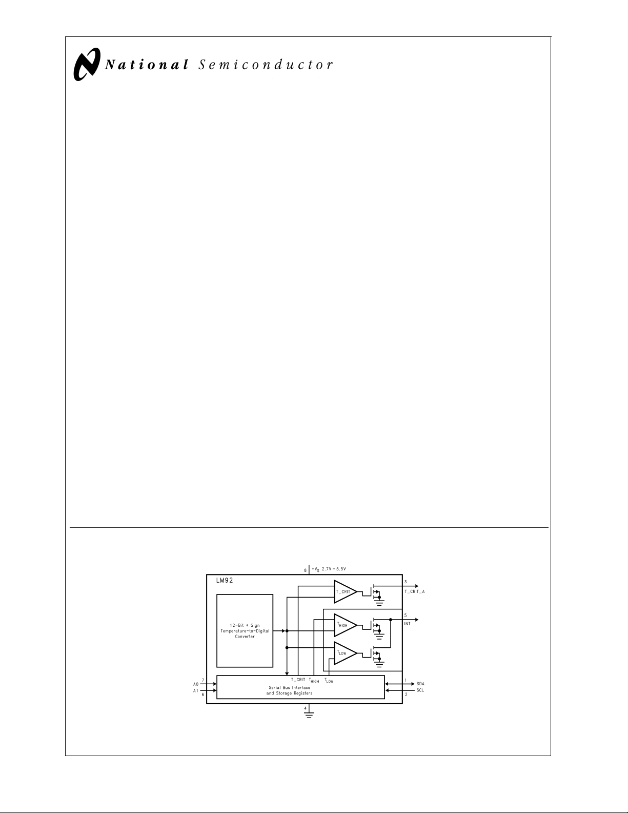
Simplified Block Diagram
DS101051-1
I2C®is a registered trademark of Philips Corporation.
© 2000 National Semiconductor Corporation DS101051 www.national.com
Page 2
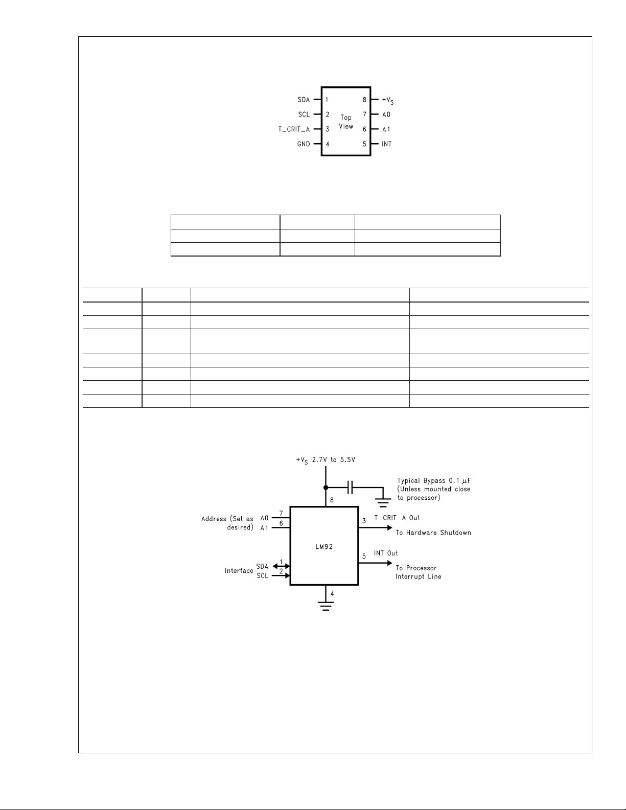
Connection Diagram
LM92
Ordering Information
Pin Descriptions
SO-8
DS101051-2
LM92
See NS Package Number M08A
Order Number Supply Voltage Supplied As
LM92CIM 2.7V to 5.5V
LM92CIMX 2.7V to 5.5V 2500 Units on Tape and Reel
Label Pin
SDA 1 Serial Bi-Directional Data Line. Open Drain Output From Controller
SCL 2 Serial Bus Clock Input From Controller
T_CRIT_A 3 Critical Temperature Alarm Open Drain Output Pull Up Resistor, Controller Interrupt Line
GND 4 Power Supply Ground Ground
INT 5 Interrupt Open Drain Output Pull Up Resistor, Controller Interrupt Line
+V
S
A0–A1 7,6 User-Set Address Inputs Ground (Low, “0”) or +V
#
8 Positive Supply Voltage Input DC Voltage from 2.7V to 5.5V
Function Typical Connection
or System Hardware Shutdown
(High, “1”)
S
Typical Application
www.national.com 2
DS101051-3
Page 3
LM92
Absolute Maximum Ratings (Note 1)
Soldering Information, Lead
Temperature
Supply Voltage −0.3 V to 6.5V
Voltage at any Pin −0.3 V
to (+V
+ 0.3V)
S
Input Current at any Pin 5mA
Package Input Current (Note 2) 20mA
T_CRIT_A and INT Output Sink
Current 10mA
SOP and MSOP Package (Note 3)
Vapor Phase (60 seconds) 215˚C
Infrared (15 seconds) 220˚C
ESD Susceptibility (Note 4)
Human Body Model 2500V
Machine Model 250V
T_CRIT_A and INT Output
Voltage 6.5V
Storage Temperature −65˚C to +125˚C
Operating Ratings(Notes 1, 5)
Specified Temperature Range T
MIN
to T
(Note 6) −55˚C to +150˚C
Supply Voltage Range (+V
) +2.7V to +5.5V
S
Electrical Characteristics
Temperature-to-Digital Converter CharacteristicsUnless otherwise noted, these specifications apply for +VS=+2.7V to +5.5V
for LM92CIM . Boldface limits apply for TA=TJ=T
Parameter Conditions
Accuracy (This is a summary. For
more detailed information please
see (Note 9))
= +30˚C, +VS= 3.3V to
T
A
4.0V
T
= 10˚C or +50˚C, +VS=
A
3.3V to 4.0V
T
= −10 ˚C or +85˚C, +VS=
A
3.3V to 4.0V
T
= +125˚C, +VS= 4.0V
A
T
= −25˚C to 150˚C, +VS=
A
4.0V
Resolution (Note 10) 13
Linearity (Note 11)
Offset Error of Transfer Function
+V
= 4.0V ˚C (max)
S
(Note 12)
Offset Error of Transfer Function
Supply Sensitivity
2.7V ≤ +V
3.6V ≤ +V
<
S
≤ 5.5V ˚C/V (max)
S
Temperature Conversion Time (Note 13) 500 1000 ms
Quiescent Current I
2
C Inactive 0.35 mA
2
I
C Active 0.35 0.625 mA (max)
Shutdown Mode 5 µA
T
Default Temperature (Notes 15, 16) 2 ˚C
HYST
T
Default Temperature (Note 16) 10 ˚C
LOW
T
Default Temperature (Note 16) 64 ˚C
HIGH
T
Default Temperature (Note 16) 80 ˚C
C
MIN
to T
; all other limits TA=TJ=+25˚C, unless otherwise noted.
MAX
Typical
(Note 7)
Limits
(Note 8)
±
0.33
±
0.50
±
1.00
±
1.25
±
1.50
Units
(Limit)
˚C (max)
Bits
0.0625
±
0.5 ˚C (max)
˚C
3.6V ˚C/V (max)
MAX
www.national.com3
Page 4
Electrical Characteristics
LM92
DIGITAL DC CHARACTERISTICSUnless otherwise noted, these specifications apply for +VS=+2.7V to +5.5V for LM92CIM .
Boldface limits apply for TA=TJ=T
Symbol Parameter Conditions
V
IN(1)
SDA and SCL Logical “1” Input
MIN
to T
; all other limits TA=TJ=+25 ˚C, unless otherwise noted.
MAX
Typical
(Note 7)
Limits
(Note 8)
+VSx 0.7 V (min)
Voltage
+V
+0.3 V (max)
S
V
IN(0)
SDA and SCL Logical “0” Input
−0.3 V (min)
Voltage
+V
x 0.3 V (max)
S
V
IN(HYST)
SDA and SCL Digital Input
500 250 mV (min)
Hysteresis
V
IN(1)
A0 and A1 Logical “1” Input
2.0 V (min)
Voltage
+V
+0.3 V (max)
S
V
IN(0)
A0 and A1 Logical “0” Input
−0.3 V (min)
Voltage
0.7 V (max)
I
I
C
I
V
IN(1)
IN(0)
IN
OH
OL
Logical “1” Input Current VIN=+V
S
0.005 1.0 µA (max)
Logical “0” Input Current VIN= 0 V −0.005 −1.0 µA (max)
Capacitance of All Digital Inputs 20 pF
High Level Output Current VOH=+V
S
10 µA (max)
Low Level Output Voltage IOL=3mA 0.4 V (max)
T_CRIT_A Output Saturation
Voltage
I
= 4.0 mA
OUT
(Note 14)
0.8 V (max)
T_CRIT_A Delay 1 Conversions
t
OF
Output Fall Time CL= 400 pF 250 ns (max)
I
=3mA
O
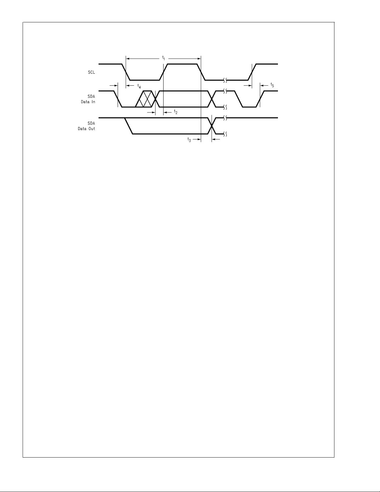
SERIAL BUS DIGITAL SWITCHING CHARACTERISTICS Unless otherwise noted, these specifications apply for +VS=+2.7V
to +5.5V for LM92CIM . Boldface limits apply for TA=TJ=T
noted. CL (load capacitance) on output lines = 80 pF unless otherwise specified. Boldface limits apply for T
T
; all other limits TA=TJ= +25 ˚C, unless otherwise noted.
MAX
The switching characteristics of the LM92 fully meet or exceed the published specifications of the I
MIN
to T
; all other limits TA=TJ=+25 ˚C, unless otherwise
MAX
2
A=TJ=TMIN
C bus. The following parameters are the timing relationship between SCL and SDA signal related to the LM92. They are not the I2C bus specifications.
Symbol Parameter Conditions
t
1
SCL (Clock) Period 2.5 µs(min)
Typical
(Note 7)
Limits
(Note 8)
1 ms(max)
t
2
t
3
t
4
t
5
t
TIMEOUT
Data in Set-Up Time to SCL High 100 ns(min)
Data Out Stable after SCL Low 0 ns(min)
SDA Low Set-Up Time to SCL Low (Start Condition) 100 ns(min)
SDA High Hold Time after SCL High (Stop Condition) 100 ns(min)
SDA and SCL Time Low for Reset of Serial Interface
(Note 17)
75
300
Units
(Limit)
(max)
to
Units
(Limit)
ms (min)
ms
(max)
www.national.com 4
Page 5
Electrical Characteristics (Continued)
Serial Bus Communication
DS101051-4
Note 1: Absolute Maximum Ratings indicate limits beyond which damage to the device may occur. DC and AC electrical specifications do not apply when operating
the device beyond its rated operating conditions.
Note 2: When the input voltage (V
maximum package input current rating limits the number of pins that can safely exceed the power supplies with an input current of 5 mA to four.
Note 3: See AN-450 “Surface Mounting Methods and Their Effect on Product Reliability” or the section titled “Surface Mount” found in a current National Semiconductor Linear Data Book for other methods of soldering surface mount devices.
Note 4: Human body model, 100 pF discharged through a 1.5 kΩ resistor. Machine model, 200 pF discharged directly into each pin.
Note 5: LM92 θ
Note 6: While the LM92 has a full-scale-range in excess of 128 ˚C, prolonged operation at temperatures above 125 ˚C is not recommended.
Note 7: Typicals are at T
Note 8: Limits are guaranteed to National’s AOQL (Average Outgoing Quality Level).
(thermal resistance, junction-to-ambient) when attached to a printed circuit board with 2 oz. foil is 200 ˚C/W.
JA
) at any pin exceeds the power supplies (V
I
= 25 ˚C and represent most likely parametric norm.
A
<
I
GND or V
>
+VS) the current at that pin should be limited to 5 mA. The 20 mA
I
LM92
www.national.com5
Page 6
Electrical Characteristics (Continued)
LM92
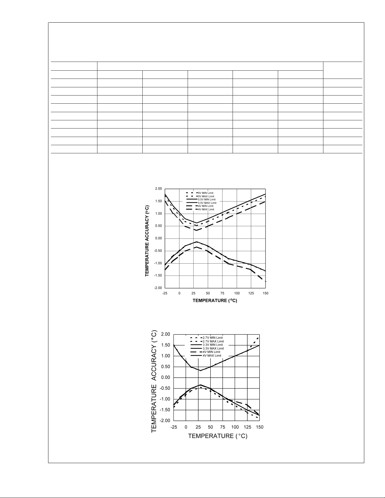
Note 9: The limits found in the following table supersede the limits shown in the Electrical Characteristics Table.The Accuracy specification includes errors due to
linearity,offset and gain. The accuracy specification includes effects of self heating with negligible digital output loading. Pull-up resistors should be maximized (10k
typical recommended), so that self heating due to digital output loading is negligible.
Temperature Accuracy Parameter Limits Units
Conditions +V
T
= −25˚C −1.35/+1.50 −1.25/+1.50 −1.25/+1.50 −1.05/+1.70 −1.05/+1.80 ˚C (max)
A
T
= −10˚C
A
T
= 0˚C −0.80/+0.75 −0.70/+0.75 −0.70/+0.75 −0.50/+0.95 −0.50/+1.05 ˚C (max)
A
T
= 10˚C −0.60/+0.50
A
T
= 30˚C −0.43/+0.33
A
T
= 50˚C −0.60/+0.50
A
T
= 85˚C −1.10/+0.85 −1.00/+0.85 −1.00/+0.85 −0.80/+1.05 −0.80/+1.15 ˚C (max)
A
T
= 125˚C −1.60/+1.25 −1.50/+1.25
A
T
= 150˚C
A
Limits at intermediate temperatures can be calculated using a straight line interpolation as shown in the following graphs:
=2.7V +VS=3.3V +VS=4V +VS=5V +VS=5.5V
S
±
1.00 −0.90/+1.00 −0.90/+1.00 −0.70/+1.20 −0.70/+1.30 ˚C (max)
±
0.50
±
0.33
±
0.50
±
1.90 −1.75/+1.50
±
0.50 −0.30/+0.70 −0.30/+0.80 ˚C (max)
±
0.33 −0.13/+0.53 −0.13/+0.63 ˚C (max)
±
0.50 −0.30/+0.70 −0.30/+0.80 ˚C (max)
±
1.25 −1.05/+1.45 −1.05/+1.55 ˚C (max)
±
1.50 −1.30/+1.70 −1.30/+1.80 ˚C (max)
Accuracy vs Temperature with +Vs=5V
Accuracy vs Temperature with +Vs= 3.3V
Note 10: 12 bits + sign, two’s complement
www.national.com 6
DS101051-20
DS101051-21
Page 7

Electrical Characteristics (Continued)
Note 11: Linearity Error is defined as the worse case difference of an actual reading to that of a calculated reading derived from the straight line whose endpoints
are measured at 30˚C and 125˚C for the range of 30˚C to 125˚C or whose endpoints are measured at 30˚C and −25˚C for the range of 30˚C to −25˚.
Note 12: Offset Error calibration should be done at 30˚C. The residual error of the transfer function is then equivalent to the Accuracy Limit minus the Offset Limit.
This does not take into account the power supply sensitivity of the offset error. Nor, does it take into account the error introduced by the calibration system used.
Note 13: This specification is provided only to indicate how often temperature data is updated. The LM92 can be read at any time without regard to conversion state
(and will yield last conversion result). If a conversion is in process it will be interrupted and restarted after the end of the read.
Note 14: For best accuracy, minimize output loading. 10k pull-ups resistors should be sufficient. Higher sink currents can affect sensor accuracy with internal heat-
ing. This can cause an error of 0.64 ˚C at full rated sink current and saturation voltage based on junction-to-ambient thermal resistance.
Note 15: Hysteresis value adds to the T
subtracts from the T
discussion of the function of hysteresis refer to
Note 16: Default values set at power up.
Note 17: Holding the SDA and/or SCL lines Low for a time interval greater than t
bus communication (SDA and SCL set High).
and T_CRIT setpoints (e.g.: if T
HIGH
setpoint value (e.g.: if T
LOW
Section 1.1
setpoint = 10 ˚C, and hysteresis = 2 ˚C, then actual hysteresis point is 10+2 = 12 ˚C); and
LOW
setpoint = 64 ˚C, and hysteresis = 2 ˚C, then actual hysteresis point is 64−2 = 62 ˚C). For a detailed
HIGH
, TEMPERATURE COMPARISON, and
TIMEOUT
Figure 3
.
will cause the LM92 to reset SCL and SDA to the IDLE state of the serial
LM92
DS101051-5
FIGURE 2. Temperature-to-Digital Transfer Function (Non-linear scale for clarity)
www.national.com7
Page 8

1.0 Functional Description
LM92
The LM92 temperature sensor incorporates a band-gap type
temperature sensor, 13-bit ADC, and a digital comparator
with user-programmable upper and lower limit values. The
comparator activates either the INT line for temperatures
outside the T
LOW
and T
window, or the T_CRIT_A line
HIGH
for temperatures which exceed T_CRIT. The lines are programmable for mode and polarity.
1.1 TEMPERATURE COMPARISON
LM92 provides a window comparison against a lower (T
and upper (T
) trip point. A second upper trip point
HIGH
(T_CRIT) functions as a critical alarm shutdown.
depicts the comparison function as well as the modes of operation.
1.1.1 STATUS BITS
The internal Status bits operate as follows:
“True”: Temperature above a T
those respective bits. A “true” for T
T
.
LOW
or T_CRIT is “true” for
HIGH
is temperature below
LOW
“False”: Assuming temperature has previously crossed
above T
low the points corresponding T
T_CRIT − T
T
LOW
T
LOW
+T
HYST
or T_CRIT, then the temperature must drop be-
HIGH
) in order for the condition to be false. For
HYST
HYST(THIGH
, assuming temperature has previously crossed below
, a “false” occurs when temperature goes above T
.
The Status bits are not affected by reads or any other actions, and always represent the state of temperature vs. setpoints.
1.1.2 HARDWIRE OUTPUTS
The T_CRIT_A hardwire output mirrors the T_CRIT_A flag,
when the flag is true, the T_CRIT_A output is asserted at all
times regardless of mode. Reading the LM92 has no effect
on the T_CRIT_A output, although the internal conversion is
restarted.
The behavior of the INT hardwire output is as follows:
Comparator Interrupt Mode (Default): User reading part
resets output until next measurement completes. If condition
is still true, output is set again at end of next conversion
cycle. For example, if a user never reads the part, and temperature goes below T
then INT becomes active. It
LOW
would stay that way until temperature goes above T
T
. However if the user reads the part, the output would
HYST
be reset. At the end of the next conversion cycle, if the condition is true, it is set again. If not, it remains reset.
Event Interrupt Mode: User reading part resets output until next condition ″event″ occurs (in other words, output is
only set once for a true condition, if reset by a read, it remains reset until the next triggering threshold has been
crossed). Conversely, if a user never read the part, the output would stay set indefinitely after the first event that set the
output. An “event” for Event Interrupt Mode is defined as:
1. Transitioning upward across a setpoint, or
2. Transitioning downward across a setpoint’s corresponding hysteresis (after having exceeded that setpoint).
For example, if a user never read the part, and temperature
went below T
then INT would become active. It would
LOW
stay that way forever if a user never read the part.
−T
LOW
Figure 3
HYST
LOW
LOW
However if the user read the part, the output would be reset.
Even if the condition is true, it will remain reset. The temperature must cross above T
LOW+THYST
to set the output
again.
In either mode, reading any register in the LM92 restarts the
conversion. This allows a designer to know exactly when the
LM92 begins a comparison. This prevents unnecessary Interrupts just after reprogramming setpoints. Typically, system Interrupt inputs are masked prior to reprogramming trip
)
points. By doing a read just after resetting trip points, but
prior to unmasking, unexpected Interrupts are prevented.
Avoid programming setpoints so close that their hysteresis
values overlap. An example would be that with a T
of 2 ˚C then setting T
HIGH
and T
to within 4 ˚C of each
LOW
HYST
value
other will violate this restriction. To be more specific, with
T
set to 2 ˚C assume T
HYST
equal to, or higher than 60 ˚C this restriction is violated.
set to 64 ˚C. If T
HIGH
LOW
is set
1.2 DEFAULT SETTINGS
The LM92 always powers up in a known state. LM92 power
up default conditions are:
1. Comparator Interrupt Mode
or
2. T
3. T
set to 10 ˚C
LOW
HIGH
set to 64 ˚C
4. T_CRIT set to 80 ˚C
5. T
HYST
set to 2 ˚C
6. INT and T_CRIT_A active low
7. Pointer set to “00”; Temperature Register
The LM92 registers will always reset to these default values
when the power supply voltage is brought up from zero volts
as the supply crosses the voltage level plotted in the following curve. The LM92 registers will reset again when the
power supply drops below the voltage plotted in this curve.
Average Power on Reset Voltage
vs Temperature
+
DS101051-18
1.3 SERIAL BUS INTERFACE
The LM92 operates as a slave on the Serial Bus, so the SCL
line is an input (no clock is generated by the LM92) and the
SDA line is a bi-directional serial data line. According to Serial Bus specifications, the LM92 has a 7-bit slave address.
The five most significant bits of the slave address are hard
wired inside the LM92 and are “10010”. The two least significant bits of the address are assigned to pins A1–A0, and are
set by connecting these pins to ground for a low, (0); or to
+V
for a high, (1).
S
www.national.com 8
Page 9

LM92
1.0 Functional Description (Continued)
Therefore, the complete slave address is:
10010A1A0
MSB LSB
DS101051-6
Note: Event Interrupt mode is drawn as if the user is reading the part. If the user doesn’t read, the outputs would go low and stay that way until the LM92 is read.
Comparator Interrupt Mode is drawn as if the user never reads the part. If the user does read, the outputs will go high once read instruction is executed and, if the
fault condition still exists, go low at the end of the next conversion.
FIGURE 3. Temperature Response Diagram
1.4 TEMPERATURE DATA FORMAT
Temperature data can be read from the Temperature and Set
Point registers; and written to the Set Point registers. Temperature data can be read at any time, although reading
faster than the conversion time of the LM92 will prevent data
from being updated. Temperature data is represented by a
13-bit, two’s complement word with an LSB (Least Significant Bit) equal to 0.0625 ˚C:
Temperature Digital Output
Binary Hex
+130˚C 0 1000 0 010 0000 08 20h
+125 ˚C 0 0111 1101 0000 07 D0h
+80 ˚C 0 0101 1010 0000 05 90h
+64 ˚C 0 0100 0000 0000 04 00h
+25 ˚C 0 0001 1001 0000 01 90h
+10 ˚C 0 0000 1010 0000 00 A0h
+2 ˚C 0 0000 0010 0000 00 20h
+0.0625 ˚C 0 0000 0000 0001 00 01h
0 ˚C 00 0000 0000 00 00h
−0.0625 ˚C 1 1111 1111 1111 1F FFh
−25 ˚C 1 1110 0111 0000 1E 70h
Temperature Digital Output
Binary Hex
−55 ˚C 1 1100 1001 0000 1C 90h
1.5 SHUTDOWN MODE
Shutdown mode is enabled by setting the shutdown bit in the
Configuration register via the Serial Bus. Shutdown mode reduces power supply current to 5 µA typical. T_CRIT_A is reset if previously set. Since conversions are stoped during
shutdown, T_CRIT_A and INT will not be operational. The
Serial Bus interface remains active.Activity on the clock and
data lines of the Serial Bus may slightly increase shutdown
mode quiescent current. Registers can be read from and
written to in shutdown mode. The LM92 takes miliseconds to
respond to the shutdown command.
1.6 INT AND T_CRIT_A OUTPUT
The INT and T_CRIT_A outputs are open-drain outputs and
do not have internal pull-ups. A ″high″ level will not be observed on these pins until pull-up current is provided from
some external source, typically a pull-up resistor. Choice of
resistor value depends on many system factors but, in general, the pull-up resistor should be as large as possible. This
will minimize any errors due to internal heating of the LM92.
www.national.com9
Page 10

1.0 Functional Description (Continued)
LM92
The maximum resistance of the pull up, based on LM92
specification for High Level Output Current, to provide a 2
volt high level, is 30K ohms.
1.7 FAULT QUEUE
A fault queue of 4 faults is provided to prevent false tripping
when the LM92 is used in noisy environments. The 4 faults
must occur consecutively to set flags as well as INT and
T_CRIT_A outputs. The fault queue is enabled by setting bit
4 of the Configuration Register high (see Section 1.11).
1.8 INTERNAL REGISTER STRUCTURE
There are four data registers in the LM92, selected by the
Pointer register.At power-up the Pointer is set to “00”; the location for the Temperature Register. The Pointer register
latches the last location it was set to. In Interrupt Mode, a
read from the LM92 resets the INT output. Placing the device
in Shutdown mode resets the INT and T_CRIT_Aoutputs. All
registers are read and write, except the Temperatureregister
which is read only.
A write to the LM92 will always include the address byte and
the Pointer byte. A write to the Configuration register requires one data byte, while the T
LOW,THIGH
, and T_CRIT
registers require two data bytes.
Reading the LM92 can take place either of two ways: If the
location latched in the Pointer is correct (most of the time it is
expected that the Pointer will point to the Temperature register because it will be the data most frequently read from the
LM92), then the read can simply consist of an address byte,
www.national.com 10
DS101051-7
followed by retrieving the corresponding number of data
bytes. If the Pointer needs to be set, then an address byte,
pointer byte, repeat start, and another address byte plus required number of data bytes will accomplish a read.
The first data byte is the most significant byte with most significant bit first, permitting only as much data as necessary to
be read to determine the temperature condition. For instance, if the first four bits of the temperature data indicates
a critical condition, the host processor could immediately
take action to remedy the excessive temperature. At the end
of a read, the LM92 can accept either Acknowledge or No
Acknowledge from the Master (No Acknowledge is typically
used as a signal for the slave that the Master has read its
last byte).
An inadvertent 8-bit read from a 16-bit register, with the D7
bit low,can cause the LM92 to stop in a state where the SDA
line is held low as shown in
Figure 4
. This can prevent any
further bus communication until at least 9 additional clock
cycles have occurred. Alternatively, the master can issue
clock cycles until SDA goes high, at which time issuing a
“Stop” condition will reset the LM92.
Page 11

1.0 Functional Description (Continued)
FIGURE 4. Inadvertent 8-Bit Read from 16-Bit Register where D7 is Zero (“0”)
LM92
DS101051-8
www.national.com11
Page 12

1.0 Functional Description (Continued)
LM92
1.9 POINTER REGISTER
(Selects which registers will be read from or written to):
P7 P6 P5 P4 P3 P2 P1 P0
00000 Register Select
P0–P2: Register Select:
P2 P1 P0 Register
0 0 0 Temperature (Read only) (Power-up
default)
0 0 1 Configuration (Read/Write)
010T
HYST
(Read/Write)
0 1 1 T_CRIT (Read/Write)
100T
101T
(Read/Write)
LOW
(Read/Write)
HIGH
1 1 1 Manufacturer’s ID
P3–P7: Must be kept zero.
1.10 TEMPERATURE REGISTER
(Read Only):
D15 D14 D13 D12 D11 D10 D9 D8 D7 D6 D5 D4 D3 D2 D1 D0
Sign MSB Bit10Bit 9 Bit 8 Bit 7 Bit 6 Bit 5 Bit 4 Bit 3 Bit 2 Bit 1 Bit 0
CRIT HIGH LOW
Status Bits
D0–D2: Status Bits
D3–D15: Temperature Data. One LSB = 0.0625˚C. Two’s complement format.
1.11 CONFIGURATION REGISTER
(Read/Write):
D7 D6 D5 D4 D3 D2 D1 D0
0 0 0 Fault Queue INT Polarity T_CRIT_A
INT Mode Shutdown
Polarity
D0: Shutdown - When set to 1 the LM92 goes to low power shutdown mode. Power up default of “0”.
D1: Interrupt mode-0isComparator Interrupt mode, 1 is Event Interrupt mode. Power up default of “0”.
D2, D3: T_CRIT_A and INT Polarity-0isactive low, 1 is active high. Outputs are open-drain. Power up default of “0”
D4: Fault Queue - When set to 1 the Fault Queu is enabled,
see
Section 1.7
. Power up default of “0”.
D5–D7: These bits are used for production testing and must be kept zero for normal operation.
1.12 T
HYST,TLOW,THIGH
AND T_CRIT_A REGISTERS
(Read/Write):
D15 D14 D13 D12 D11 D10 D9 D8 D7 D6 D5 D4 D3 D2 D1 D0
Sign MSB Bit10Bit 9 Bit 8 Bit7 Bit6 Bit5 Bit 4 Bit 3 Bit 2 Bit 1 Bit 0 X X X
D0–D2: Undefined
D3–D15: T
T
HYST
T
HYST
HYST,TLOW,THIGH
= 2˚C.
is subtracted from T
Avoid programming setpoints so close that their hysteresis values overlap. See
or T_CRIT TripTemperature Data. Power up default is T
, and T_CRIT, and added to T
HIGH
LOW
.
= 10˚C, T
LOW
Section 1.1
= 64˚C, T_CRIT = 80˚C,
HIGH
.
www.national.com 12
Page 13

1.0 Functional Description (Continued)
1.13 Manufacturer’s Identification Register
(Read only):
D15 D14 D13 D12 D11 D10 D9 D8 D7 D6 D5 D4 D3 D2 D1 D0
1000000000000001
D0–D15: Manufactures ID.
LM92
www.national.com13
Page 14

2.0 I2C Timing Diagrams
LM92
Typical 2-Byte Read From Preset Pointer Location Such as Temp or Comparison Registers
Typical Pointer Set Followed by Immediate Read for 2-Byte Register such as Temp or Comparison Registers
DS101051-9
DS101051-10
DS101051-11
Typical 1-Byte Read from Configuration Register with Preset Pointer
Typical Pointer Set Followed by Immediate Read from Configuration Register
Configuration Register Write
Comparison Register Write
FIGURE 6. Timing Diagrams
DS101051-12
DS101051-13
DS101051-14
www.national.com 14
Page 15

3.0 Application Hints
The temperature response graph in
cal application designed to meet ACPI requirements. In this
type of application, the temperature scale is given an arbitrary value of ″granularity″, or the window within which temperature notification events should occur. The LM92 can be
programmed to the window size chosen by the designer,and
will issue interrupts to the processor whenever the window
limits have been crossed. The internal flags permit quick determination of whether the temperature is rising or falling.
The T_CRIT limit would typically use its separate output to
activate hardware shutdown circuitry separate from the processor. This is done because it is expected that if temperature has gotten this high that the processor may not be responding. The separate circuitry can then shut down the
system, usually by shutting down the power supply.
Note that the INT and T_CRIT_A outputs are separate, but
can be wire-or’d together. Alternatively the T_CRIT_A can be
diode or’d to the INT line in such a way that a T_CRIT_A
event activates the INT line, but an INT event does not activate the T_CRIT_A line. This may be useful in the event that
it is desirable to notify both the processor and separate
T_CRIT_A shutdown circuitry of a critical temperature alarm
at the same time (maybe the processor is still working and
can coordinate a graceful shutdown with the separate shutdown circuit).
Figure 7
depicts a typi-
To implement ACPI compatible sensing it is necessary to
sense whenever the temperature goes outside the window,
issue an interrupt, service the interrupt, and reprogram the
window according to the desired granularity of the temperature scale. The reprogrammed window will now have the current temperature inside it, ready to issue an interrupt whenever the temperature deviates from the current window.
To understand this graph, assume that at the left hand side
the system is at some nominal temperature. For the 1st
event temperature rises above the upper window limit,
T
, causing INT to go active. The system responds to the
HIGH
interrupt by querying the LM92’s status bits and determines
that T
was exceeded, indicating that temperature is ris-
HIGH
ing. The system then reprograms the temperature limits to a
value higher by an amount equal to the desired granularity.
Note that in Event Interrupt Mode, reprogramming the limits
has caused a second, known, interrupt to be issued since
temperature has been returned within the window. In Comparator Interrupt Mode, the LM92 simply stops issuing interrupts.
The 2nd event is another identical rise in temperature. The
3rd event is typical of a drop in temperature. This is one of
the conditions that demonstrates the power of the LM92, as
the user receives notification that a lower limit is exceeded in
such a way that temperature is dropping.
The Critical Alarm Event activates the separate T_CRIT_A
output. Typically, this would feed circuitry separate from the
processor on the assumption that if the system reached this
temperature, the processor might not be responding.
LM92
DS101051-15
Note: Event Interrupt mode is drawn as if the user is reading the part. If the user doesn’t read, the outputs would go low and stay that way until the LM92 is read.
FIGURE 7. Temperature Response Diagram for ACPI Implementation
www.national.com15
Page 16

4.0 Typical Applications
LM92
DS101051-16
FIGURE 8. Typical Application
FIGURE 9. Remote HVAC temperature sensor communicates via 3 wires, including thermostat signals.
www.national.com 16
DS101051-17
Page 17

4.0 Typical Applications (Continued)
DS101051-19
FIGURE 10. ACPI Compatible Terminal Alarm Shutdown. By powering the LM92 from auxilary output of the power
supply, a non-functioning overheated computer can be powered down to preserve as much of the system as
possible.
LM92
www.national.com17
Page 18

Physical Dimensions inches (millimeters) unless otherwise noted
Two-Wire Interface
8-Lead (0.150" Wide) Molded Small Outline Package (SOP), JEDEC
Order Number LM92CIM or LM92CIMX
NS Package Number M08A
LIFE SUPPORT POLICY
NATIONAL’S PRODUCTS ARE NOT AUTHORIZED FOR USE AS CRITICAL COMPONENTS IN LIFE SUPPORT
DEVICES OR SYSTEMS WITHOUT THE EXPRESS WRITTEN APPROVAL OF THE PRESIDENT AND GENERAL
COUNSEL OF NATIONAL SEMICONDUCTOR CORPORATION. As used herein:
1. Life support devices or systems are devices or
systems which, (a) are intended for surgical implant
into the body, or (b) support or sustain life, and
whose failure to perform when properly used in
accordance with instructions for use provided in the
2. A critical component is any component of a life
support device or system whose failure to perform
can be reasonably expected to cause the failure of
the life support device or system, or to affect its
safety or effectiveness.
labeling, can be reasonably expected to result in a
significant injury to the user.
0.33˚C Accurate, 12-Bit + Sign Temperature Sensor and Thermal Window Comparator with
±
National Semiconductor
Corporation
Americas
Tel: 1-800-272-9959
Fax: 1-800-737-7018
Email: support@nsc.com
www.national.com
National Semiconductor
Europe
Fax: +49 (0) 180-530 85 86
Email: europe.support@nsc.com
Deutsch Tel: +49 (0) 69 9508 6208
English Tel: +44 (0) 870 24 0 2171
Français Tel: +33 (0) 1 41 91 8790
National Semiconductor
Asia Pacific Customer
Response Group
Tel: 65-2544466
Fax: 65-2504466
Email: ap.support@nsc.com
National Semiconductor
Japan Ltd.
Tel: 81-3-5639-7560
Fax: 81-3-5639-7507
LM92
National does not assume any responsibility for use of any circuitry described, no circuit patent licenses are implied and National reserves the right at any time without notice to change said circuitry and specifications.
 Loading...