

Page 1
August 2001
LM88
Factory Programmable Dual Remote-Diode Thermostat
LM88 Factory Programmable Dual Remote-Diode Thermostat
General Description
The LM88 is a dual remote-diode temperature sensor with 3
digital comparators. The LM88 has 3 open-drain outputs
(O_SP0, O_SP1 and O_CRIT) that can be used as interrupts or to signal system shutdown. The digital comparators
can be factory programmed to make a greater than or less
than comparison. When programmed for a greater than
comparison outputs:
O_SP0 and O_SP1 activate when the temperatures measured by D0 or D1 exceed the associated setpoints of
T_SP0 or T_SP1.
O_CRIT activates when the temperature measured by
either D0 or D1 exceeds setpoint T_CRIT.
T_CRIT can be set at 1˚C intervals from −40˚C to +125˚C.
T_SP0 andT_SP1 can be set at 4˚C intervals in the range of
T_CRIT +127˚C/−128˚C. Hysteresis for all comparators is
set to 1˚C. O_CRIT, in conjunction with T_CRIT, could be
used to prevent catastrophic damage to key subsystems
such as notebook Card Bus cards while O_SP0 and O_SP1,
in conjunction with T_SP0 and T_SP1, can warn of an
impending failure.
The LM88 is available in an 8-lead mini-small-outline package.
Applications
n Microprocessor Thermal Management
n Appliances
n Portable Battery Powered Systems
n Fan Control
n Industrial Process Control
n HVAC Systems
n Remote Temperature Sensing
n Electronic System Protection
Features
n 2 external remote diode input channels
n 3 digital comparator outputs, 1 per remote diode and
one T_CRIT common to both
n Factory programmable greater than or less than
comparisons
n 1˚C comparator hysteresis
n 2 setpoints, T_SP0 and T_SP1, factory programmable in
4˚C intervals
n 1 setpoint, T_CRIT, factory programmable in 1˚C
intervals
n Active Low open-drain digital outputs
n 8-pin mini-SO plastic package
Key Specifications
j
Power Supply Voltage 2.8V–3.8V
j
Power Supply Current 1.5 mA (max)
j
LM88 Temperature Range −40˚C to +85˚C
j
Diode Setpoint Temperature
Range 0˚C to +125˚C
j
Temperature Trip PointAccuracy:
Diode Junction
Temperature
)
(T
DJ
+45˚C to +85˚C
+60˚C to +100˚C
Note: These are sample ranges. Contact factory for other
ranges.
LM88CIM
Accuracy
±
3˚C (max) −40˚C to +85˚C
±
3˚C (max) −40˚C to +85˚C
LM88CIM
Temperature
Range
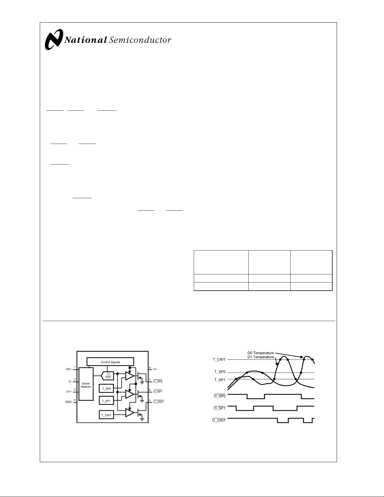
Simplified Block Diagram and Connection Diagram
MSOP-8/MUA08A Package
Top View
10132601
© 2001 National Semiconductor Corporation DS101326 www.national.com
For simplicity, the effects of the hysteresis are not shown in the
temperature response diagram.
10132602
Page 2
Simplified Block Diagram and Connection Diagram (Continued)
LM88
Order Number Device
Marking
LM88CIMM-A
LM88CIMMX-A Tape and
LM88CIMM-B
LM88CIMMX-B Tape and
For other setpoints please contact the factory. Performance is dependent on temperature range.
T08A
T08A
NS Package
Number
MUA08A
or
MSOP-8
MUA08A
or
MSOP-8
Transport
Media
Rail
Real
Rail
Real
T_SP0
(˚C)
61 49 80
41 49 60
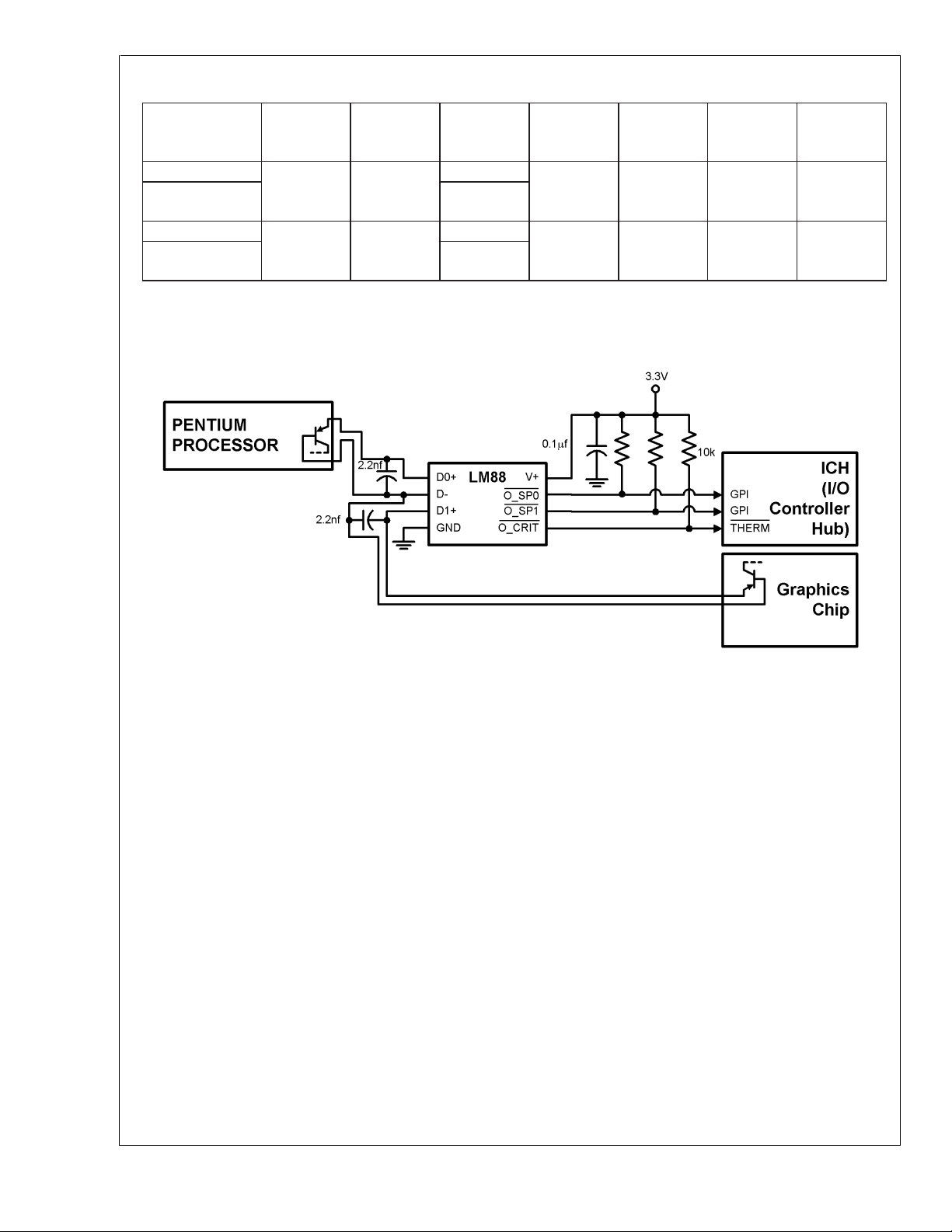
Typical Application
T_SP1
(˚C)
T_CRIT
(˚C)
S etpoint
Accuracy
(˚C)
±
3
±
3
FIGURE 1. Thermal Protection for Pentium®Processor and Graphics Chip
10132613
www.national.com 2
Page 3

LM88
Absolute Maximum Ratings (Note 1)
Input Voltage 6V
Input Current at any pin (Note 2) 5mA
Package Input Current (Note 2) 20mA
Package Dissipation at T
(Note 4) 900mW
Soldering Information
MSOP Package (Note 6) :
= 25˚C
A
Operating Ratings(Note 1)
Operating Temperature
Range T
LM88CIMM −40˚C ≤ TA≤ +85˚C
Remote Diode Junction 0˚C ≤ T
Positive Supply Voltage (V
Maximum V
and V
O_CRIT,VO_SP0
O_SP1
+
) +2.8V to +3.8V
MIN
≤ T ≤ T
≤ +125˚C
DJ
Vapor Phase (60 seconds) 215˚C
Infrared (15 seconds) 220˚C
Storage Temperature −65˚C to + 150˚C
ESD Susceptibility (Note 5)
Human Body Model
Machine Model
2500V
250V
LM88 Electrical Characteristics
The following specifications apply for 2.8VDC≤V+≤ 3.8VDCunless otherwise specified. Boldface limits apply for TA=TJ=
T
to T
MIN
Symbol Parameter Conditions (Note 7) Limits (Limits)
Temperature Sensor
V
D−,VD0
I
D+SOURCE
V
D−Out
; all other limits TA=TJ= 25˚C unless otherwise specified.
MAX
Typical LM88CIMM Units
(Note 8)
Setpoint Temperature Accuracy (Note 9) +60˚C ≤ T
+45˚C ≤ T
+30˚C ≤ T
≤ +100˚C
DJ
≤ +85˚C
DJ
≤ +70˚C
DJ
±
3 ˚C (max)
Setpoint Hysteresis 1 ˚C (min)
1 ˚C (max)
Output Update Rate 920 ms (max)
and VD1Analog Inputs
Diode Source Current (D+ − D−)=0.65; high
level
(D+ − D−)=0.65; low
level
120 210 µA (max)
46 µA (min)
12 21 µA (max)
4.6 µA (min)
D− Output Source Voltage 0.7 V
MAX
+5.5V
LM88 Electrical Characteristics
The following specifications apply for 2.8VDC≤V+≤ 3.8VDCunless otherwise specified. Boldface limits apply for TA=TJ=
T
to T
MIN
Symbol Parameter Conditions Typical Limits Units
+
V
Power Supply
Digital Outputs
I
OUT(“1”)
V
OUT(“0”)
Note 1: Absolute Maximum Ratings indicate limits beyond which damage to the device may occur. Operating Ratings indicate conditions for which the device is
functional, but do not guarantee specific performance limits. For guaranteed specifications and test conditions, see the Electrical Characteristics. The guaranteed
specifications apply only for the test conditions listed. Some performance characteristics may degrade when the device is not operated under the listed test
conditions.
; all other limits TA=TJ= 25˚C unless otherwise specified.
MAX
I
S
Supply Current 1.5 mA (max)
Logical “1” Output Leakage
Current (Note 10)
V
where V
2.8V
V
2.8V
Logical “0” Output Voltage I
(Note 7) (Note 8) (Limits)
=V+− 0.6V
OUT
+
=3.8V to
=V+=3.8V to
OUT
=+3mA 0.4 V (max)
OUT
2 µA (max)
40 µA (max)
www.national.com3
Page 4

LM88 Electrical Characteristics (Continued)
LM88
Note 2: When the input voltage (VI) at any pin exceeds the power supply (V
maximum package input current rating limits the number of pins that can safely exceed the power supplies with an input current of 5mA to four.
Note 3: Parasitics or ESD protectioncircuitryareshownin the diagram found below.The ESD Clamp circtuitry is triggered on when there is an ESD event. The table
maps what devices appear on the different pins.
<
I
GND or V
>
V+), the current at that pin should be limited to 5mA. The 20mA
I
Pin Name D1 D2 D3 D4 D5 D6 R1
D0+ XXXX X50Ω
D− XXXXXX50Ω
D1+ XXXX X50Ω
O_CRIT
O_SP1
O_SP0
XXXX 0Ω
XXXX 0Ω
XXXX 0Ω
10132604
Note 4: The maximum power dissipation must be derated at elevated temperatures and is dictated by T
ambient thermal resistance) and T
given in the Absolute Maximum Ratings, whichever is lower. For this device, T
package types when board mounted follow:
(ambient temperature). The maximum allowable power dissipation at any temperature is PD=(T
A
Package Type θ
= 125˚C. For this device the typical thermal resistance (θJA) of the different
Jmax
JA
(maximum junction temperature), θJA(junction to
Jmax
)/θJAor the number
Jmax–TA
MUA08A 250˚C/W
Note 5: The human body model is a 100pF capacitor discharged through a 1.5kΩ resistor into each pin. The machine model is a 200pF capacitor discharged directly
into each pin.
Note 6: See the URL ”http://www.national.com/packaging/“ for other recomdations and methods of soldering surface mount devices.
Note 7: Typicals are at T
Note 8: Limits are guaranteed to National’s AOQL (Average Outgoing Quality Level).
Note 9: These are sample temperature ranges, contact the factory for other temperature ranges. Performance is dependent on temperature range.
Note 10: The two I
current, 2µA (max). In Region 2, V
current flow is under short circuit conditions as specified at 40µA (max). Under normal operating conditions a pull-resistor (R) will be used. The voltage drop across
this pull-up resistor caused by the 2µA normal leakage current with large values of R (much greater than 100k) will bias diode D1 into the cutoff region causing the
additional current to be negligible in the voltage drop calculation. With low values of R more current will flow as in the case of a 1.1k pull-up, 20µA may flow causing
less than 22mV of voltage drop.
specifications are intended to describe two operating regions of the output voltage. In Region 1, V+− 0.6V and below, there is normal leakage
OH
= 25˚C and represent most likely parametric norm.
J=TA
+
− 0.6V to V+, there is additional current flowing caused by the ESD protection circuitry (see Figure in Note 3). The maximum
www.national.com 4
Page 5

1.0 Functional Description
LM88
a) When programmed for a greater than comparison
10132611
FIGURE 2. Comparator output temperature response diagrams
1.1 PIN DESCRIPTIONS
+
V
This is the positive supply voltage pin, which has
a range of 2.8 to 3.8 volts. This pin should be
bypassed with a 0.1µF capacitor to ground.
GND This is the ground pin.
D0+, D1+ These pins connect to the positive terminal of the
diodes (e.g. a 2N3904 collector base shorted or a
Pentium thermal diode anode) and provide the
source current for forward biasing the diodes for
the temperature measurement. During a tem-
perature conversion, the current source switches
between 120µA and 12µA. The diodes are
sampled sequentially.
D− This pin should be connected to the negative pin
of each diode (e.g. a 2N3904 emitter or a Pen-
tium thermal diode cathode). A star connection is
recommended. Separate traces should be routed
from this pin to each diode cathode. This pin
biases the negative diode terminals to approxi-
mately 0.7V.
O_CRIT
This is an active-low open-drain digital output. It
goes LOW when a comparison of either diode
temperature reading to the setpoint T_CRIT is
true. It returns to HIGH when the comparison of
the diode temperature, that caused the true con-
b) When programmed for a less than comparison
±
dition, to T_CRIT
1˚C is false. The CRIT comparator can be factory programmed to make a
greater than or less than comparison. (See Section 1.3 LM88 OPTIONS)
O_SP1
This is an active-low open-drain digital output. It
goes LOW when the comparison of the temperature reading of diode one to the value of T_SP1 is
true. The SP1 comparator has a built in hysteresis of 1˚C. Therefore, O_SP1 returns to HIGH
when diode one’s temperature comparison to the
value of T_SP1
±
1˚C is false. The SP1 comparator can be factory programmed to make a greater
than or less than comparison.(See Section 1.3
LM88 OPTIONS)
O_SP0
This is an active-low open-drain digital output. It
goes LOW when the comparison of the temperature reading of diode one to the value of T_SP0 is
true. The SP0 comparator has a built in hysteresis of 1˚C. Therefore, O_SP0 returns to HIGH
when diode one’s temperature comparison to the
value of T_SP0
±
1˚C is false. The SP0 comparator can be factory programmed to make a greater
than or less than comparison.(See Section 1.3
LM88 OPTIONS)
10132612
www.national.com5
Page 6

1.0 Functional Description (Continued)
LM88
1.2 TYPICAL PIN CONNECTION
Pin Label Pin Number Typical Connection
D0+ 1 3904-type transistor
D− 2 3904-type transistor emitter or
D1+ 3 3904-type transistor shorted
GND 4 a quiet system ground
O_CRIT
O_SP1
O_SP1
+
V
shorted-collector base or
Pentium thermal diode anode;
2.2nF capacitor connected to
D-
Pentium thermal diode
cathode (individual traces are
required to each diode; do not
daisy chain); two 2.2nF
capacitors connected to D0+
and D1+
collector-base or Pentium
thermal diode anode; 2.2nF
capacitor connected to D-
5 2k pull-up; system shutdown
or the THERM pin of the ICH
(I/O Controller Hub found in
PCs)
6 2k pull-up; general purpose
input (GPI), to determine
which diode caused the
THERM event
7 2k pull-up; general purpose
input (GPI), to determine
which diode caused the
THERM event
8 3.3V; 0.1µF bypass capacitor
1.3 LM88 OPTIONS
1.3.1 Set-Point Values
T_SP0 and T_SP1 are dependent on the value of T_CRIT:
T_SP0 = T_CRIT + 4a + 1
T_SP1 = T_CRIT + 4b + 1
where:
a and b are any integer in the range of −32 to +31.
T_CRIT can be any value in the range of 0˚C to +125˚C with
a resolution of 1˚C.
1.3.2 Functionality
The LM88’s comparators can be factory programmed to do a
greater than or less than comparison. When programmed for
a greater than comparison, the comparison result is true
when the temperature measured is above the preprogrammed setpoint temperature. The comparison returns to
false when the temperature measured is below or equal to
the setpoint temperature minus one degree. For a less than
comparison the comparison result is true when the temperature measured is below the preprogrammed limit. The result
turns to false when the temperature measured is above or
equal to the setpoint limit plus one degree. SP0, SP1 and
CRIT comparisons can all be independently programmed to
www.national.com 6
be greater than or less than. All CRIT comparisons are
required to be the same, either greater than or less than. The
comparator hysteresis can also be factory set to one, two or
three degrees. The hysteresis for all comparisons is required
to be the same.
2.0 Application Hints
2.1 OPEN-DRAIN OUTPUTS
The O_SP0, O_SP1 and 0_CRIT outputs are open-drain
outputs and do not have internal pull-ups. A “high” level will
not be observed on these pins until pull-up current is provided from some external source, typically a pull-up resistor.
Choice of resistor value depends on many system factors
but, in general, the pull-up resistor should be as large as
possible. This will minimize any internal temperature reading
errors due to internal heating of the LM88. The maximum
resistance of the pull-up needed to provide a 2.1V high level,
based on LM88 specification for High Level Output Current
with the supply voltage at 3.0V, is 430kΩ.
2.2 THERMAL DIODE MOUNTING CONSIDERATIONS
To measure temperature the LM88 uses two remote diodes.
These diodes can be located on the die of a target IC,
allowing measurement of the IC’s temperature, independent
Page 7

2.0 Application Hints (Continued)
of the LM88’s temperature. The LM88 has been optimized to
measure the remote diode of a Pentium type processor as
shown in
sense the temperature of external objects or ambient air.
Remember that a discrete diode’s temperature will be affected, and often dominated, by the temperature of its leads.
As with any IC, the LM88 and accompanying wiring and
circuits must be kept insulated and dry, to avoid leakage and
corrosion. This is especially true if the circuit may operate at
cold temperatures where condensation can occur.
Printed-circuit coatings and varnishes such as Humiseal and
epoxy paints or dips are often used to ensure that moisture
cannot corrode the LM88 or its connections. Moisture may
also cause leakage on the diode wiring and therefore affect
the accuracy of the temperature set-points.
Most silicon diodes do not lend themselves well to this
application. It is recommended that a 2N3904 transistor
base emitter junction be used with the collector tied to the
base.
A diode connected 2N3904 approximates the junction available on a Pentium III microprocessor for temperature measurement. Therefore, the LM88 can sense the temperature
of this diode effectively.
2.3 EFFECTS OF THE DIODE NON-IDEALITY FACTOR ON ACCURACY
The technique used in today’s remote temperature sensors
is to measure the change in V
points of a diode. For a bias current ratio of N:1, this difference is given as:
where:
The temperature sensor then measures ∆V
to IT digital data. In this equation, k and q are well defined
universal constants, and N is a parameter controlled by the
Figure 3
. A discrete diode can also be used to
10132615
FIGURE 3. Pentium or 3904 Temperature vs LM88
Temperature Set-point
at two different operating
BE
— η is the non-ideality factor of the process the diode is
manufactured on,
— q is the electron charge,
— k is the Boltzmann’s constant,
— N is the current ratio,
— T is the absolute temperature in ˚K.
and converts
BE
temperature sensor. The only other parameter is η, which
depends on the diode that is used for measurement. Since
is proportional to both η and T, the variations in η
∆V
BE
cannot be distinguished from variations in temperature.
Since the non-ideality factor is not controlled by the temperature sensor, it will directly add to the inaccuracy of the
sensor. For the Pentium II, Intel specifies a
±
1% variation in
η from part to part. As an example, assume a temperature
sensor has an accuracy specification of
±
3 ˚C at room
temperature of 25 ˚C and the process used to manufacture
the diode has a non-ideality variation of
±
1%. The resulting
accuracy of the temperature sensor at room temperature will
be:
T
=±3˚C+(±1% of 298 ˚K) =±6˚C
ACC
.
The additional inaccuracy in the temperature measurement
caused by η can be eliminated if each temperature sensor is
calibrated with the remote diode that it will be paired with.
2.4 PCB LAYOUT to MINIMIZE NOISE
In a noisy environment, such as a processor motherboard,
layout considerations are very critical. Noise induced on
traces running between the remote temperature diode sensor and the LM88 can cause temperature conversion errors.
The following guidelines should be followed:
1. Place a 0.1 µF power supply bypass capacitor as close
as possible to the V
pin and the recommended 2.2 nF
DD
capacitor as close as possible to the D+ and D− pins.
Make sure the traces to the two 2.2nF capacitor are
matched.
2. The recommended 2.2nF diode bypass capacitor actu-
ally has a range of 200pF to 3.3nF. The average temperature accuracy will not change over that capacitance
range. Increasing the capacitance will lower the corner
frequency where differential noise error will start to affect
the temperature reading thus producing a reading that is
more stable. Conversely, lowering the capacitance will
increase the corner frequency where differential noise
error starts to affect the temperature reading thus producing a reading that is less stable.
3. Ideally, the LM88 should be placed within 10cm of the
remote diode pins with the traces being as straight, short
and identical as possible. Trace resistance of 1Ω can
cause as much as 1˚C of error. This error can be compensated by using the Remote Temperature Offset Registers, since the value placed in these registers will
automatically be subtracted or added to the remote temperature reading.
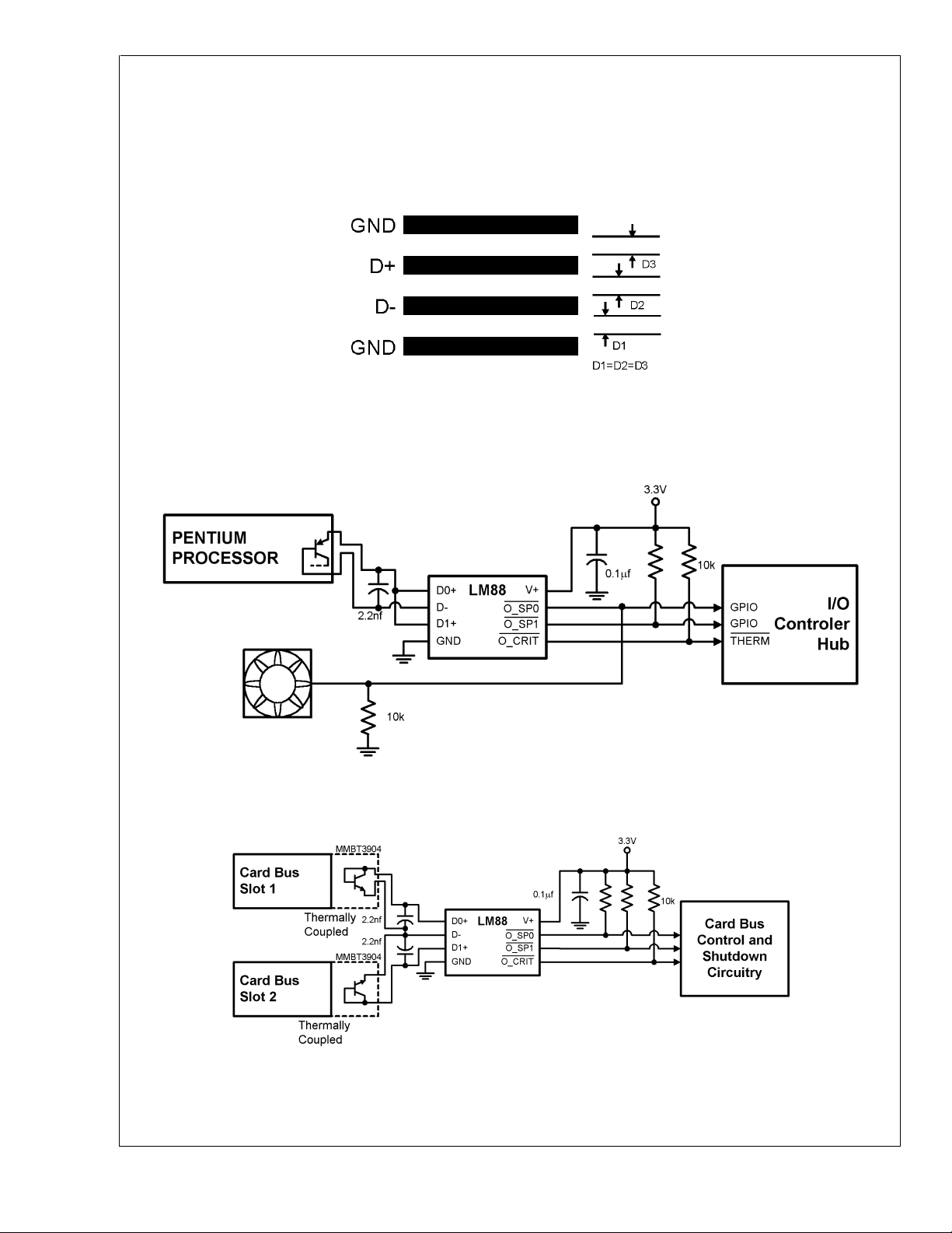
4. Diode traces should be surrounded by a GND guard ring
to either side, above and below if possible. This GND
guard should not go between the D+ and D− lines so
that in the event that noise does couple to the diode
lines, it would be coupled common mode and rejected.(See
Figure 4
)
5. Avoid routing diode traces in close proximity to power
supply switching or filtering inductors.
6. Avoid running diode traces close to or parallel to high
speed digital and bus lines. Diode traces should be kept
at least 2cm apart from the high speed digital traces.
7. If it is necessary to cross high speed digital traces, the
diode traces and the high speed digital traces should
cross at a 90 degree angle.
LM88
www.national.com7
Page 8
2.0 Application Hints (Continued)
LM88
8. The ideal place to connect the LM88’s GND pin is as
close as possible to the processor GND associated with
the sense diode.
9. Leakage current between D+ and GND should be kept
to a minimum. One nano-ampere of leakage can cause
FIGURE 4. Ideal Diode Trace Layout
3.0 Applications Circuits
as much as 1˚C of error in the diode temperature reading. Keeping the printed circuit board as clean as possible will minimize leakage current.
10132633
FIGURE 5. Pentium processor Thermal Management with Fan Control
FIGURE 6. Card Bus Thermal Management
www.national.com 8
10132614
10132603
Page 9
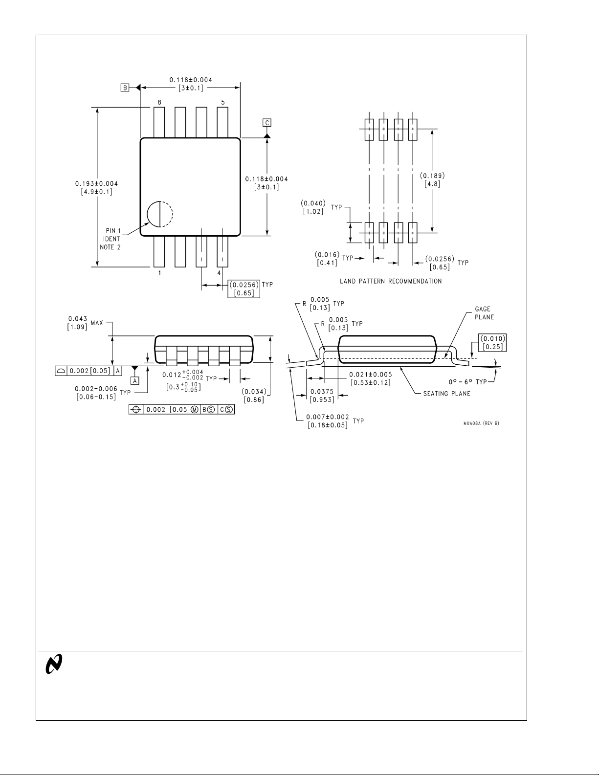
Physical Dimensions inches (millimeters)
unless otherwise noted
LM88 Factory Programmable Dual Remote-Diode Thermostat
8-Lead Molded Mini Small Outline Package (MSOP)
(JEDEC REGISTRATION NUMBER M0-187)
Order Number LM88CIMM, or LM88CIMMX
NS Package Number MUA08A
LIFE SUPPORT POLICY
NATIONAL’S PRODUCTS ARE NOT AUTHORIZED FOR USE AS CRITICAL COMPONENTS IN LIFE SUPPORT
DEVICES OR SYSTEMS WITHOUT THE EXPRESS WRITTEN APPROVAL OF THE PRESIDENT AND GENERAL
COUNSEL OF NATIONAL SEMICONDUCTOR CORPORATION. As used herein:
1. Life support devices or systems are devices or
systems which, (a) are intended for surgical implant
into the body, or (b) support or sustain life, and
whose failure to perform when properly used in
accordance with instructions for use provided in the
2. A critical component is any component of a life
support device or system whose failure to perform
can be reasonably expected to cause the failure of
the life support device or system, or to affect its
safety or effectiveness.
labeling, can be reasonably expected to result in a
significant injury to the user.
National Semiconductor
Corporation
Americas
Email: support@nsc.com
www.national.com
National Semiconductor
Europe
Fax: +49 (0) 180-530 85 86
Email: europe.support@nsc.com
Deutsch Tel: +49 (0) 69 9508 6208
English Tel: +44 (0) 870 24 0 2171
Français Tel: +33 (0) 1 41 91 8790
National Semiconductor
Asia Pacific Customer
Response Group
Tel: 65-2544466
Fax: 65-2504466
Email: ap.support@nsc.com
National Semiconductor
Japan Ltd.
Tel: 81-3-5639-7560
Fax: 81-3-5639-7507
National does not assume any responsibility for use of any circuitry described, no circuit patent licenses are implied and National reserves the right at any time without notice to change said circuitry and specifications.
 Loading...