

Page 1
July 2000
LM84
Diode Input Digital Temperature Sensor with Two-Wire
Interface
General Description
The LM84 is a remote diode temperature sensor,
Delta-Sigma analog-to-digital converter, and digital
over-temperature detector with an SMBus
LM84 senses its own temperature as well as the temperature of a target IC with a diode junction, such as a Pentium
II processor or a diode connected 2N3904. A diode junction
(semiconductor junction) is required on the target IC’s die. A
host can query the LM84 at any time to read the temperature
of this diode as well as the temperature state of the LM84
itself.AT_CRIT_A interrupt output becomes active when the
temperature is greater than a programmable comparator
limit, T_CRIT.
The host can program as well as read back the state of the
T_CRIT register. Three state logic inputs allow two pins
(ADD0,ADD1) to select up to 9 SMBus address locations for
the LM84. The sensor powers up with default thresholds of
127˚C for T_CRIT.
™
interface. The
Features
n Directly senses die temperature of remote ICs
n Senses temperature of remote diodes
n SMBus compatible interface, supports SMBus Timeout
n Register readback capability
n 7 bit plus sign temperature data format
n 2 address select lines enable 9 LM84s to be connected
to a single bus
®
Key Specifications
j
Supply Voltage 3.0V - 3.6V
j
Supply Current 1 mA (max)
j
Local Temperature Accuracy
j
Remote Diode Temperature Accuracy
+60˚C to +100˚C
0˚C to +125˚C
Applications
n System Thermal Management
n Personal Computers
n Electronic Test Equipment
n Office Electronics
n HVAC
±
1.0˚C (typ)
±
3˚C (max)
±
5˚C (max)
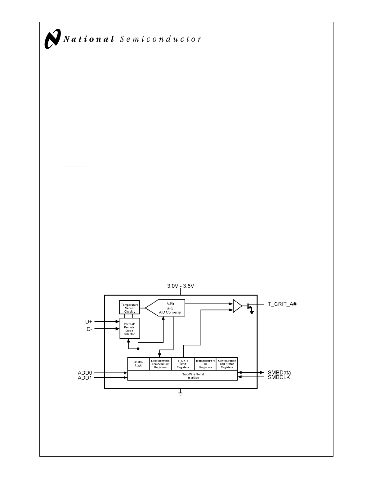
LM84 Diode Input Digital Temperature Sensor with Two-Wire Interface
Simplified Block Diagram
#
Indicates Active Low (”NOT“)
SMBus™is a trademark of the Intel Corporation.
®
Pentium
II processor is a registered trademark of the Intel Corporation.
®
I2C
is a registered trademark of the Philips Corporation.
DS100961-1
© 2001 National Semiconductor Corporation DS100961 www.national.com
Page 2
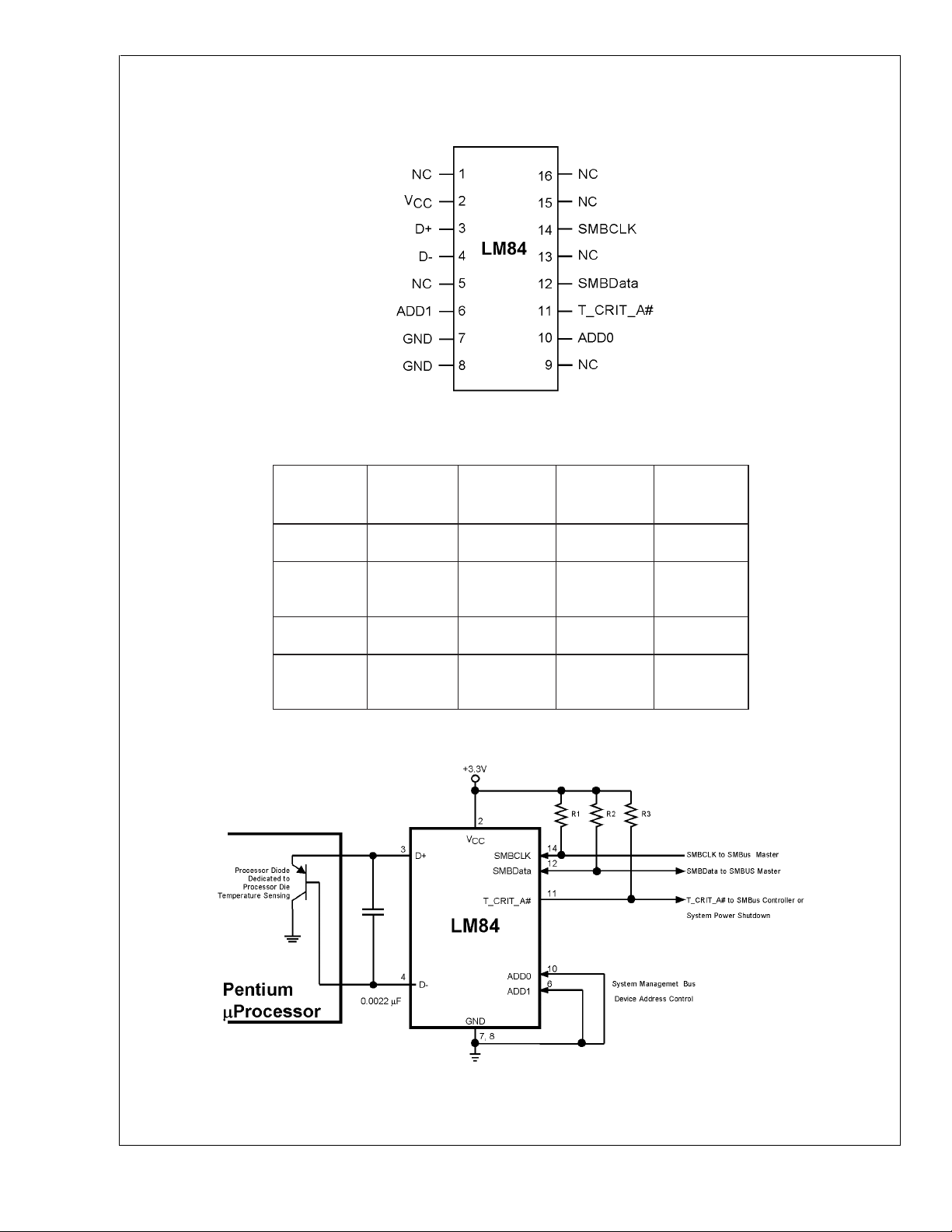
Connection Diagram
LM84
Ordering Information
QSOP-16
DS100961-2
TOP VIEW
Order
Number
LM84BIMQA
LM84BIMQAX
LM84CIMQA
LM84CIMQAX
Typical Application
NS
Package
Number
MQA16A
(QSOP-16)
MQA16A
(QSOP-16)
MQA16A
(QSOP-16)
MQA16A
(QSOP-16)
Transport
Media
95 Units in
Rail
2500 Units on
Tape and
Reel
95 Units in
Rail
2500 Units on
Tape and
Reel
SMBus
Revision
Level
1.1 20MHz
1.1 20MHz
1.0 Not Available
1.0 Not Available
Noise Filter
on SMBCLK
www.national.com 2
DS100961-3
Page 3
Pin Descriptions
LM84
Label Pin
#
Function Typical Connection
Manufacturing test pins. Left floating. PC board traces may be routed
NC
V
CC
1, 5, 9,
13, 16
2
Positive Supply Voltage
Input
Diode Current Source To Diode Anode. Connected to remote discrete
D+ 3
D− 4
ADD0–ADD1 10, 6
Diode Return Current
Sink
User-Set SMBus (I
2
Address Inputs
C)
GND 7, 8 Power Supply Ground Ground
T_CRIT_A
SMBData 12
11
Critical Temperature
Alarm, open-drain output
SMBus (I
2
C) Serial
Bi-Directional Data Line,
open-drain output
2
SMBCLK 14 SMBus (I
NC 15
No Connection Left floating. PC board traces may be routed
C) Clock Input From Controller
through the pads for these pins. Although, the
components that drive these traces should share
the same supply as the LM84 so that the Absolute
Maximum Voltage at any Pin rating is not violated.
DC Voltage from 3.0V to 3.6V
diode or to the diode on the external IC whose die
temperature is being sensed.
To Diode Cathode. Must be grounded when not
used.
Ground (Low, “0”), VCC(High, “1”) or open
(“TRI-LEVEL”)
Pull Up Resistor, Controller Interrupt Line or
System Shutdown
From and to Controller, Pull Up Resistor
through the pads for this pin.
www.national.com3
Page 4
Absolute Maximum Ratings (Note 1)
LM84
Supply Voltage −0.3V to 6.0V
Voltage at Any Pin:
NC (Pins 1,5,9), ADD0, ADD1, D
+
All other pins (except D−) −0.3V to 6.0V
D− Input Current
(V
−0.3V to
+ 0.3V)
CC
±
1mA
Soldering Information, Lead Temperature
QSOP Package (Note 3)
Vapor Phase (60 seconds) 215˚C
Infrared (15 seconds) 220˚C
ESD Susceptibility (Note 4)
Human Body Model 2500V
Machine Model 250V
Input Current at All Other Pins (Note
2) 5 mA
Package Input Current (Note 2) 20 mA
SMBData, T_CRIT_A Output Sink
Current 10 mA
Output Voltage 6.0V
Storage Temperature −65˚C to +150˚C
Operating Ratings
(Note 1) and (Note 5)
Specified Temperature Range T
LM84 0˚C to +125˚C
Supply Voltage Range (V
) +3.0V to +3.6V
CC
Temperature-to-Digital Converter Characteristics
Unless otherwise noted, these specifications apply for VCC=+3.0 Vdc to +3.6 Vdc. Boldface limits apply for TA=TJ=T
to T
Local Temperature Error (Note 8)
Remote Temperature Error using
Pentium Diode (Note 8) and (Note
9)
Remote Temperature Error using
Diode Connected 2N3904 (Note 8)
and (Note 9)
Resolution 8 Bits
Temperature Conversion Time (Note 11) 120 145 ms
Quiescent Current (Note 10) SMBus (I
D− Source Voltage 0.7 V
Diode Source Current (D+ − D−)=+ 0.65V; high
T_CRIT_A Output Saturation
Voltage
Power-On Reset Threshold On V
Local and Remote T_CRIT Default
Temperature
; all other limits TA=TJ=+25˚C, unless otherwise noted.
MAX
Parameter Conditions Typical Limits Units
(Note 6) (Note 7) (Limit)
±
1˚C
+60˚C ≤T
= 3.3 Vdc
V
CC
0˚C ≤ T
= 3.3 Vdc
V
CC
+60˚C ≤T
= 3.3 Vdc
V
CC
0˚C ≤ T
= 3.3 Vdc
V
CC
≤ +100˚C,
A
≤ +125˚C,
A
≤ +100˚C,
A
≤ +125˚C,
A
±
3
±
5 ˚C (max)
+1, −5 ˚C (max)
+3, −7 ˚C (max)
1˚C
2
C Inactive) 0.500 1 mA (max)
160 µA (max)
level
50 µA (min)
Low level 16 µA (max)
5 µA (min)
I
= 3.0 mA 0.4
OUT
edge
input, falling
CC
2.2
1.2
(Note 12) +127 ˚C
to T
MIN
˚C (max)
V (max)
V (max)
V (min)
MAX
MIN
www.national.com 4
Page 5
Logic Electrical Characteristics
DIGITAL DC CHARACTERISTICS
Unless otherwise noted, these specifications apply for V
T
; all other limits TA=TJ=+25˚C, unless otherwise noted.
MAX
Symbol Parameter Conditions Typical LM84B LM84C Units
SMBData, SMBCLK
V
V
I
I
IN(1)
IN(0)
IN(1)
IN(0)
Logical “1” Input Voltage 2.1 1.4 V (min)
Logical “0”Input Voltage 0.8 0.6 V (max)
Logical “1” Input Current VIN=V
Logical “0” Input Current VIN= 0V −0.005 −1.0 −1.0 µA (max)
ADD0, ADD1
V
V
I
I
IN(1)
IN(0)
IN(1)
IN(0)
Logical “1” Input Voltage V
Logical “0”Input Voltage GND 0.5 0.5 V (max)
Logical “1” Input Current VIN=V
Logical “0” Input Current VIN=0V 50 600 600 µA (max)
ALL DIGITAL INPUTS
C
IN
Input Capacitance 20 pF
ALL DIGITAL OUTPUTS
I
OH
V
OL
High Level Output Current VOH=V
SMBus Low Level Output
Voltage
=+3.0 to 3.6 Vdc. Boldface limits apply for TA=TJ=T
CC
(Note 6) Limits
(Note 7)
CC
CC
CC
IOL=3mA
=6mA
I
OL
0.005 1.0 1.0 µA (max)
CC
1.6 1.6 V (min)
50 600 600 µA (max)
100 100 µA (max)
0.4
0.6
Limits
(Note 7)
0.4
0.6
MIN
V (max)
LM84
to
(Limit)
www.national.com5
Page 6

Logic Electrical Characteristics (Continued)
LM84
SMBus DIGITAL SWITCHING CHARACTERISTICS
Unless otherwise noted, these specifications apply for V
pF. Boldface limits apply for T
A=TJ=TMIN
to T
The switching characteristics of the LM84 fully meet or exceed the published specifications of the SMBus or I
lowing parameters are the timing relationships between SMBCLK and SMBData signals related to the LM84. They are not necessarily the I
2
C or SMBus bus specifications.
=+3.0 Vdc to +3.6 Vdc, CL(load capacitance) on output lines = 80
CC
; all other limits TA=TJ= +25˚C, unless otherwise noted.
MAX
2
C bus. The fol-
Symbol Parameter Conditions Typical Limits Units
(Note 6) (Note 7) (Limit)
f
SMB
SMBus Clock Frequency 400
10
t
LOW
SMBus Clock Low Time 10% to 10% 1.3
25
t
SEXT Cumulative Clock Low Extend Time 25 ms (max)
LOW
t
HIGH
t
R;SMB
t
F;SMB
t
OF
t
TIMEOUT
t
1
t
,
2
t
SU;DAT
t
,
3
t
HD;DAT
t
,
4
t
HD;STA
t
,
5
t
SU;STO
t
,
6
t
SU;STA
t
BUF
SMBus Clock High Time 90% to 90% 0.6 µs (min)
SMBus Rise Time 10% to 90% 1 µs
SMBus Fall Time 90% to 10% 0.3 µs
Output Fall Time CL= 400 pF
=3mA
I
O
SMBData and SMBCLK Time Low for
Reset of Serial Interface (Note 13)
250 ns (max)
25
40
SMBCLK (Clock) Period 2.5 µs (min)
Data In Setup Time to SMBCLK High 100 ns (min)
Data Out Stable after SMBCLK Low 0
0.9
SMBData Low Setup Time to SMBCLK
100 ns (min)
Low
SMBData High Delay Time after
100 ns (min)
SMBCLK High (Stop Condition Setup)
SMBus Start-Condition Setup Time 0.6 µs (min)
SMBus Free Time 1.3 µs (min)
kHz (max)
kHz (min)
µs (min)
ms (max)
ms (min)
ms (max)
ns (min)
µs (max)
SMBus Communication
www.national.com 6
DS100961-4
Page 7

Logic Electrical Characteristics (Continued)
SMBus TIMEOUT
LM84
DS100961-13
www.national.com7
Page 8
Logic Electrical Characteristics (Continued)
LM84
Note 1: Absolute Maximum Ratings indicate limits beyond which damage to the device may occur.DC and AC electrical specifications do not apply when operating
the device beyond its rated operating conditions.
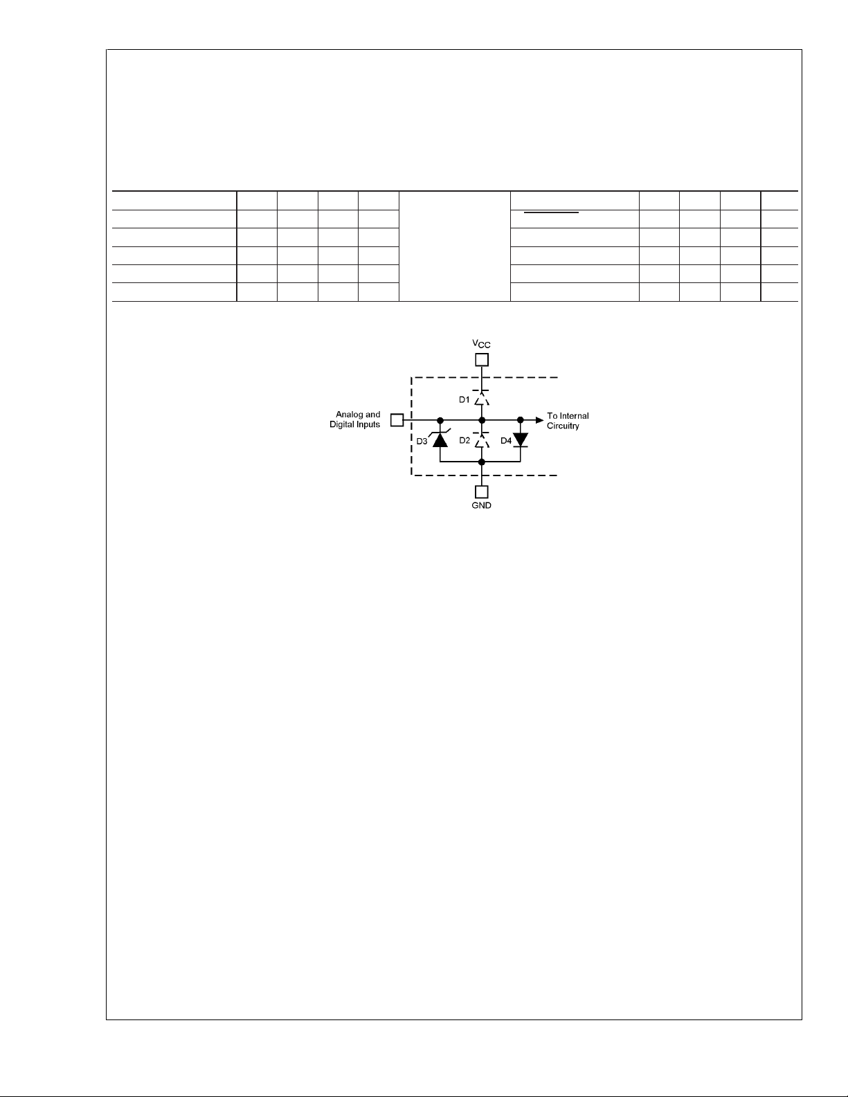
Note 2: When the input voltage (V
maximum package input current rating limits the number of pins that can safely exceed the power supplies with an input current of 5 mA to four.
Parasitics and or ESD protection circuitry are shown in the figure below for the LM84’s pins. The nominal breakdown voltage of the zener D3 is 6.5V. Care should
be taken not to forward bias the parasitic diode, D1, present on pins: NC pins 1,5 and 9, D+, ADD1 and ADD0. Doing so by more than 50 mV may corrupt a
temperature or voltage measurement.
) at any pin exceeds the power supplies (V
I
<
I
GND or V
>
VCC), the current at that pin should be limited to 5 mA. The 20 mA
I
Pin Name D1 D2 D3 D4 Pin Name D1 D2 D3 D4
NC (pins 1, 5, 9) x x x T_CRIT_A
V
CC
x SMBData x x
x
D+ x x x NC (pin 13) x x
D− x x x SMBCLK x
ADD0, ADD1 x x x NC (pin 16) x
Note: An x indicates that the diode exists.
DS100961-8
FIGURE 1. ESD Protection Input Structure
Note 3: See AN-450 “Surface Mounting Methods and Their Effect on Product Reliability” or the section titled “Surface Mount” found in a current National
Semiconductor Linear Data Book for other methods of soldering surface mount devices.
Note 4: Human body model, 100 pF discharged through a 1.5 kΩ resistor. Machine model, 200 pF discharged directly into each pin.
Note 5: Thermal resistance of the QSOP-16 package is TBD ˚C/W, junction-to-ambient when attached to a printed circuit board with 2 oz. foil.
Note 6: Typicals are at T
Note 7: Limits are guaranteed to National’s AOQL (Average Outgoing Quality Level).
Note 8: The Temperature Error specification does not include an additional error of
Note 9: The Temperature Error will vary less than
Note 10: Quiescent current will not increase substantially with an active SMBus.
Note 11: This specification is provided only to indicate how often temperature data is updated. The LM84 can be read at any time without regard to conversion state
(and will yield last conversion result).
Note 12: Default values set at power up.
Note 13: Holding the SMBData and/or SMBCLK lines Low for a time interval greater than t
state of an SMBus communication (SMBCLK and SMBData set High).
= 25˚C and represent most likely parametric norm.
A
±
1.0˚C for a variation in VCCof 3V to 3.6V from the nominal of 3.3V.
±
1˚C, caused by the quantization error.
will cause the LM84 to reset SMBData and SMBCLK to the IDLE
TIMEOUT
www.national.com 8
Page 9

Logic Electrical Characteristics (Continued)
FIGURE 2. Temperature-to-Digital Transfer Function (Non-linear scale for clarity)
1.0 Functional Description
The LM84 temperature sensor incorporates a band-gap type
temperature sensor using a Local or Remote diode and an
8-bit ADC (Delta-Sigma Analog-to-Digital Converter). The
LM84 is compatible with the serial SMBus and I
faces. Digital comparators compare Local and Remote read-
ings to user-programmable setpoints (LT_CRIT and
RT_CRIT). Activation of the T_CRIT_A output indicates that
a temperature reading is greater than the limit preset in a
T_CRIT register.
2
C inter-
LM84
DS100961-5
1.1 T_CRIT_A OUTPUT, T_CRIT LIMITS
T_CRIT_A is activated when the Local temperature reading
is greater than the limit preset in the local critical temperature
setpoint register (LT_CRIT) or when the Remote tempera-
ture reading is greater than the limit preset in the remote
critical temperature setpoint register (RT_CRIT), as shown in
Figure 3
Register) when set will disable the T_CRIT_A output.
The Status Register can be read to determine which event
caused the alarm. A bit in the Status Register is set high to
indicate T_CRIT temperature alarm, see
Local and remote temperature diodes are sampled alter-
nately by the A/D converter. The T_CRIT_A output and the
Status Register flags are updated at the completion of a
conversion, which takes approximately 60 ms. T_CRIT_A
and the Status Register flags are reset only after the Status
Register is read and if the temperature is below the setpoint.
. The T_CRIT_A mask bit (bit 7 of the Configuration
Section 1.8.3
.
DS100961-6
FIGURE 3. T_CRIT_A Temperature Response Diagram
1.2 POWER-ON RESET DEFAULT STATES
LM84 always powers up to these known default states:
1. Local Temperature set to 0˚C
2. Remote Temperature set to 0˚C until the LM84 senses a
diode present or open circuit on the D+ and D− input
pins.
3. Status Register set to 00h.
4. Command Register set to 00h; T_CRIT_A enabled.
5. Local and Remote T_CRIT set to 127˚C
www.national.com9
Page 10

1.0 Functional Description (Continued)
LM84
1.3 SMBus INTERFACE
The LM84 operates as a slave on the SMBus, so the
SMBCLK line is an input (no clock is generated by the LM84)
and the SMBData line is bi-directional. According to SMBus
specifications, the LM84 has a 7-bit slave address. Bit 4 (A3)
of the slave address is hard wired inside the LM84 to a 1.
The remainder of the address bits are controlled by the
address select pins ADD1 and ADD0, and are set by connecting these pins to ground for a low, (0) , to V
(1), or left floating (TRI-LEVEL).
Therefore, the complete slave address is:
A6 A5 A4 A3 A2 A1 A0
MSB LSB
and is selected as follows:
Address Select Pin State LM84 SMBus
Slave Address
ADD0 ADD1 A6:A0 binary
0 0 001 1000
0 TRI-LEVEL 001 1001
0 1 001 1010
TRI-LEVEL 0 010 1001
TRI-LEVEL TRI-LEVEL 010 1010
TRI-LEVEL 1 010 1011
1 0 100 1100
1 TRI-LEVEL 100 1101
1 1 100 1110
The LM84 latches the state of the address select pins during
the first read or write on the SMBus. Changing the state of
the address select pins after the first read or write to any
device on the SMBus will not change the slave address of
the LM84.
for a high,
CC
minimize any local temperature reading errors due to self
heating of the LM84. The maximum resistance of the pull-up,
based on LM84 specification for High Level Output Current,
to provide a 2V high level, is 30 kΩ.
1.6 DIODE FAULT DETECTION
Before each remote conversion the LM84 goes through an
external diode fault detection sequence. If the D+ input is
shorted to V
be +127˚C, bit 2 (OPEN) of the Status Register will be set. If
the Remote T_CRIT setpoint is set to less than +127˚C then
bit 4 (RTCRIT) of the Status Register will be set which will
activate the T_CRIT_A output, if enabled. If D+ is shorted to
GND or D−, the temperature reading will be 0˚C and bit 2 of
the Status Register will not be set.
or floating then the temperature reading will
CC
1.4 TEMPERATURE DATA FORMAT
Temperature data can be read from the Local Temperature,
Remote Temperature, and T_CRIT setpoint registers. Temperature data can only be written to the T_CRIT setpoint
registers. Temperature data is represented by an 8-bit, two’s
complement byte with an LSB (Least Significant Bit) equal to
1˚C:
Temperature Digital Output
Binary Hex
+125˚C 0111 1101 7Dh
+25˚C 0001 1001 19h
+1˚C 0000 0001 01h
0˚C 0000 0000 00h
−1˚C 1111 1111 FFh
−25˚C 1110 0111 E7h
−55˚C 1100 1001 C9h
1.5 OPEN-DRAIN OUTPUTS
SMBData and T_CRIT_A outputs are open-drain and do not
have internal pull-ups. A “high” level will not be observed on
these pins until pull-up current is provided from some external source, typically a pull-up resistor. Choice of resistor
value depends on many system factors but, in general, the
pull-up resistor should be as large as possible. This will
www.national.com 10
Page 11

1.0 Functional Description (Continued)
1.7 COMMUNICATING with the LM84
LM84
There are 10 data registers in the LM84, selected by the
Command Register. At power-up the Command Register is
set to “00”, the location for the Read Local Temperature
Register. The Command Register latches whatever the last
location it was set to. Reading the Status Register resets
T_CRIT_A. All registers are predefined as read only or write
only.Read and write registers with the same function contain
mirrored data.
AWrite to the LM84 will always include the address byte and
the command byte. A write to any register requires one data
byte.
Reading the LM84 can take place either of two ways:
1. If the location latched in the Command Register is correct (most of the time it is expected that the Command
Register will point to one of the Read Temperature Registers because that will be the data most frequently read
from the LM84), the read can simply consist of an address byte, followed by retrieving the data byte.
2. If the Command Register needs to be set, then an
address byte, command byte, repeat start, and another
address byte will accomplish a read.
The data byte has the most significant bit first. At the end of
a read, the LM84 can accept either Acknowledge or No
Acknowledge from the Master (No Acknowledge is typically
used as a signal for the slave that the Master has read its
last byte).
DS100961-9
1.7.1 SMBus TIMEOUT
The LM84 SMBus interface circuitry will be reset to the
SMBus idle state if the SMBData or SMBCLK lines are held
low for more than 40 ms. The LM84 may or may not reset the
state SMBData or SMBCLK if either of these lines are held
low between 25 ms and 40 ms. Holding SMBData or SMBCLK low for less than or equal to 25 ms will not reset the
interface circuitry. The LM84 has a built-in internal timer to
guarantee that the interface is reset if the SMBData line were
to get stuck low. This can commonly occur when the master
is reset while the slave is transmitting low. This enhancement to the SMBus TIMEOUT specification ensures error
free performance even in remote systems where complete
power supply shutdown, for reset, is a nuisance. This would
have to occur since many cost effective temperature sensors
such as the LM84 do not have a pin dedicated for reset.
www.national.com11
Page 12

1.0 Functional Description (Continued)
LM84
1.8 LM84 REGISTERS
1.8.1 COMMAND REGISTER
Selects which registers will be read from or written to. Data for this register should be transmitted during the Command Byte of
the SMBus write communication.
P7 P6 P5 P4 P3 P2 P1 P0
0000 Command Select
P0-P7: Command Select:
Command Se-
lect Address
<
P7:P0>hex
00h 0000 0000 0 RLT Read Local Temperature
01h 0000 0000 0 RRT Read Remote Temperature
02h 0000 0000 0 RS Read Status
03h 0000 0000 0 RC Read Configuration
04h 0000 0000 0 RMID Manufacturers ID
05h 0111 1111 127 RLCS Read Local T_CRIT Setpoint
07h 0111 1111 127 RRCS Read Remote T_CRIT
09h 0000 0000 0 WC Write Configuration
0Bh 0111 1111 127 WLCS Write Local T_CRIT Setpoint
0Dh 0111 1111 127 WRCS Write Remote T_CRIT
1.8.2 LOCAL and REMOTE TEMPERATURE REGISTERS
(Read Only Address 00h and 01h):
D7 D6 D5 D4 D3 D2 D1 D0
MSB Bit 6 Bit 5 Bit 4 Bit 3 Bit 2 Bit 1 LSB
D7–D0: Temperature Data. One LSB = 1˚C. Two’s complement format.
1.8.3 STATUS REGISTER
(Read Only Address 02h):
D7 D6 D5 D4 D3 D2 D1 D0
0 LTCRIT 0 RTCRIT 0 OPEN 0 0
Power up default is with all bits “0” (zero).
D2: OPEN: When set to 1 indicates a Remote Diode disconnect.
D4: RTCRIT: When set to 1 indicates an RT_CRIT alarm.
D6: LTCRIT: When set to 1 indicates an LT_CRIT alarm.
D7, D5, D3, D1–D0: These bits are always set to 0.
1.8.4 Manufacturers ID Register
(Read Address 04h) Default value 00h.
Power On Default State Register Name Register Function
<
D7:D0>binary
<
D7:D0>deci-
mal
Setpoint
Setpoint
1.8.5 CONFIGURATION REGISTER
(Read Address 03h /Write Address 09h):
D7 D6 D5 D4 D3 D2 D1 D0
T_CRIT_A
mask
Power up default is with all bits “0” (zero).
D7: T_CRIT_A mask: When set to 1 T_CRIT_A interrupts are masked.
D6–D0: These bits are always set to 0. A write of 1 will return a 0 when read.
www.national.com 12
0000000
Page 13

1.0 Functional Description (Continued)
1.8.6 LOCAL AND REMOTE T_CRIT REGISTERS
(Read/Write):
D7 D6 D5 D4 D3 D2 D1 D0
MSB Bit 6 Bit 5 Bit 4 Bit 3 Bit 2 Bit 1 LSB
D7–D0: RT_CRIT and LT_CRIT setpoint temperature data. Power up default is LT_CRIT = RT_CRIT = 127˚C.
2.0 SMBus Timing Diagrams
LM84
DS100961-10
(a) Serial Bus Write to the internal Command Register followed by a the Data Byte
DS100961-11
(b) Serial Bus Write to the internal Command Register
DS100961-12
(c) Serial Bus Read from a Register with the internal Command Register preset to desired value.
FIGURE 4. Serial Bus Timing Diagrams
www.national.com13
Page 14
3.0 Application Hints
LM84
The LM84 can be applied easily in the same way as other
integrated-circuit temperature sensors, and its remote diode
sensing capability allows it to be used in new ways as well.
It can be soldered to a printed circuit board, and because the
path of best thermal conductivity is between the die and the
pins, its temperature will effectively be that of the printed
circuit board lands and traces soldered to the LM84’s pins.
This presumes that the ambient air temperature is almost the
same as the surface temperature of the printed circuit board;
if the air temperature is much higher or lower than the
surface temperature, the actual temperature of the of the
LM84 die will be at an intermediate temperature between the
surface and air temperatures. Again, the primary thermal
conduction path is through the leads, so the circuit board
temperature will contribute to the die temperature much
more strongly than will the air temperature.
To measure temperature external to the LM84’s die, use a
remote diode. This diode can be located on the die of a
target IC, allowing measurement of the IC’s temperature,
independent of the LM84’s temperature. The LM84 has been
optimized to measure the remote diode of a Pentium II
processor as shown in
Figure 5
.A discrete diode can also be
used to sense the temperature of external objects or ambient
air. Remember that a discrete diode’s temperature will be
affected, and often dominated, by the temperature of its
leads.
where:
η is the non-ideality factor of the process the diode is
•
manufactured on,
q is the electron charge,
•
k is the Boltzmann’s constant,
•
N is the current ratio,
•
T is the absolute temperature in ˚K.
•
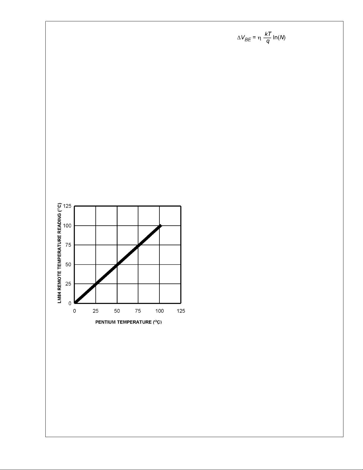
The temperature sensor then measures ∆V
and converts
BE
to digital data. In this equation, k and q are well defined
universal constants, and N is a parameter controlled by the
temperature sensor. The only other parameter is η, which
depends on the diode that is used for measurement. Since
∆V
is proportional to both η and T, the variations in η
BE
cannot be distinguished from variations in temperature.
Since the non-ideality factor is not controlled by the temperature sensor, it will directly add to the inaccuracy of the
sensor. For the Pentium II Intel specifies a
±
1% variation in
η from part to part. As an example, assume a temperature
sensor has an accuracy specification of
±
3˚C at room temperature of 25˚C and the process used to manufacture the
diode has a non-ideality variation of
±
1%. The resulting
accuracy of the temperature sensor at room temperature will
be:
T
=±3˚C+(±1% of 298˚K) =±6˚C.
ACC
The additional inaccuracy in the temperature measurement
caused by η, can be eliminated if each temperature sensor is
calibrated with the remote diode that it will be paired with.
DS100961-16
Pentium Temperature vs LM84 Temperature Reading
Most silicon diodes do not lend themselves well to this
application. It is recommended that a 2N3904 transistor
base emitter junction be used with the collector tied to the
base.
A diode connected 2N3904 approximates the junction available on a Pentium microprocessor for temperature measurement. Therefore, the LM84 can sense the temperature of this
diode effectively.
3.1 ACCURACY EFFECTS OF DIODE NON-IDEALITY
FACTOR
The technique used in today’s remote temperature sensors
is to measure the change in V
at two different operating
BE
points of a diode. For a bias current ratio of N:1, this difference is given as:
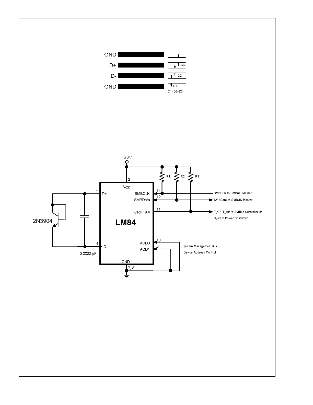
3.2 PCB LAYOUT for MINIMIZING NOISE
In a noisy environment, such as a processor mother board,
layout considerations are very critical. Noise induced on
traces running between the remote temperature diode sensor and the LM84 can cause temperature conversion errors.
The following guidelines should be followed:
1. Place a 0.1 µF power supply bypass capacitor as close
as possible to the V
pin and the recommended 2.2 nF
CC
capacitor as close as possible to the D+ and D− pins.
Make sure the traces to the 2.2 nF capacitor are
matched.
2. Ideally, the LM84 should be placed within 10 cm of the
Processor diode pins with the traces being as straight,
short and identical as possible.
3. Diode traces should be surrounded by a GND guard ring
to either side, above and below if possible. This GND
guard should not be between the D+ and D− lines. In the
event that noise does couple to the diode lines it would
be ideal if it is coupled common mode. That is equally to
the D+ and D− lines.(See
Figure 6
)
4. Avoid routing diode traces in close proximity to power
supply switching or filtering inductors.
5. Avoid running diode traces close to or parallel to high
speed digital and bus lines. Diode traces should be kept
at least 2 cm. apart from the high speed digital traces.
6. If it is necessary to cross high speed digital traces, the
diode traces and the high speed digital traces should
cross at a 90 degree angle.
www.national.com 14
Page 15
3.0 Application Hints (Continued)
7. The ideal place to connect the LM84’s GND pin is as
close as possible to the Processors GND associated
FIGURE 6. Recommended Diode Trace Layout
LM84
with the sense diode. For the Pentium II this would be
pin A14.
DS100961-15
Noise on the digital lines, overshoot greater than V
undershoot less than GND, may prevent successful SMBus
communication with the LM84. SMBus no acknowledge is
the most common symptom, causing unnecessary traffic on
the bus. Although, the SMBus maximum frequency of com-
and
CC
4.0 Typical Applications
munication is rather low (400 kHz max) care still needs to be
taken to ensure proper termination within a system with
multiple parts on the bus and long printed circuit board
traces.
Using a Diode Connected 2N3904 as a Remote Temperture Sensing Element
DS100961-17
www.national.com15
Page 16

Physical Dimensions inches (millimeters) unless otherwise noted
16-Lead QSOP Package
Order Number LM84BIMQA, LM84BIMQAX, LM84CIMQA or LM84CIMQAX
NS Package Number MQA16
LM84 Diode Input Digital Temperature Sensor with Two-Wire Interface
LIFE SUPPORT POLICY
NATIONAL’S PRODUCTS ARE NOT AUTHORIZED FOR USE AS CRITICAL COMPONENTS IN LIFE SUPPORT
DEVICES OR SYSTEMS WITHOUT THE EXPRESS WRITTEN APPROVAL OF THE PRESIDENT AND GENERAL
COUNSEL OF NATIONAL SEMICONDUCTOR CORPORATION. As used herein:
1. Life support devices or systems are devices or
systems which, (a) are intended for surgical implant
into the body, or (b) support or sustain life, and
whose failure to perform when properly used in
accordance with instructions for use provided in the
2. A critical component is any component of a life
support device or system whose failure to perform
can be reasonably expected to cause the failure of
the life support device or system, or to affect its
safety or effectiveness.
labeling, can be reasonably expected to result in a
significant injury to the user.
National Semiconductor
Corporation
Americas
Tel: 1-800-272-9959
Fax: 1-800-737-7018
Email: support@nsc.com
www.national.com
National Semiconductor
Europe
Fax: +49 (0) 180-530 85 86
Email: europe.support@nsc.com
Deutsch Tel: +49 (0) 69 9508 6208
English Tel: +44 (0) 870 24 0 2171
Français Tel: +33 (0) 1 41 91 8790
National Semiconductor
Asia Pacific Customer
Response Group
Tel: 65-2544466
Fax: 65-2504466
Email: ap.support@nsc.com
National Semiconductor
Japan Ltd.
Tel: 81-3-5639-7560
Fax: 81-3-5639-7507
National does not assume any responsibility for use of any circuitry described, no circuit patent licenses are implied and National reserves the right at any time without notice to change said circuitry and specifications.
 Loading...