

Page 1
October 2002
LM75
Digital Temperature Sensor and Thermal Watchdog with
Two-Wire Interface
General Description
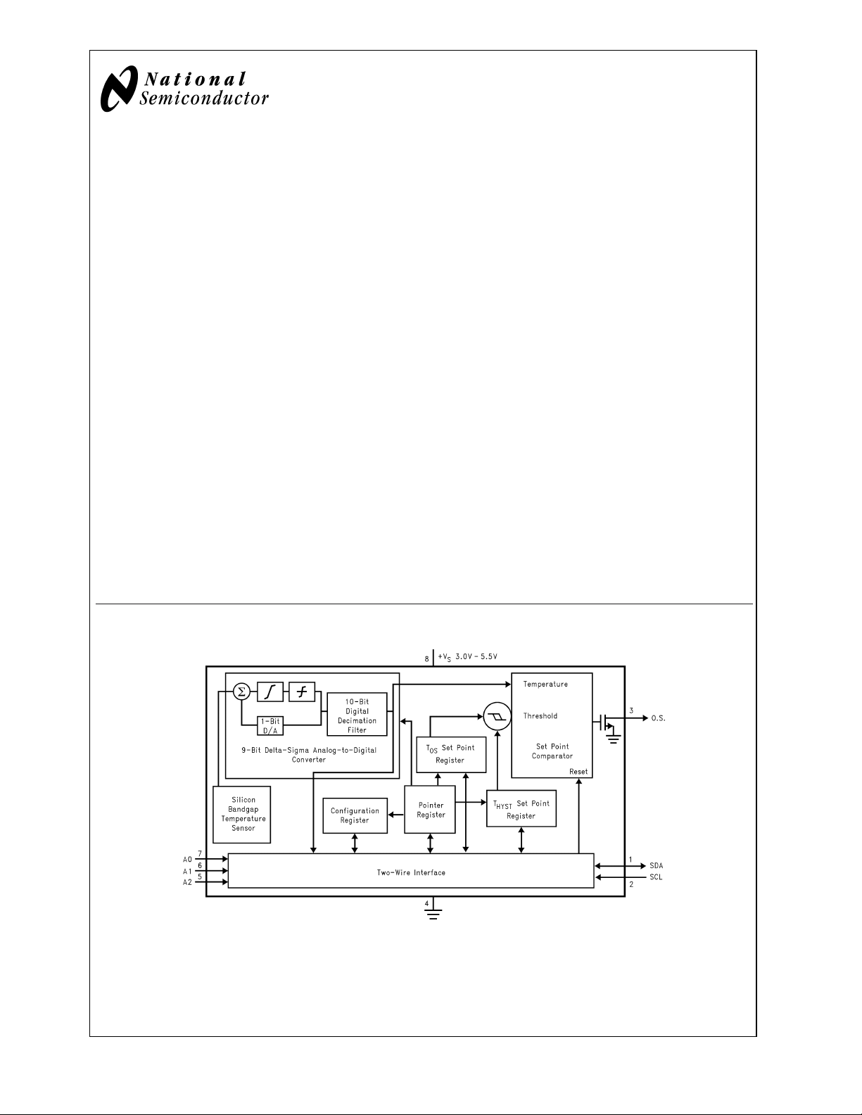
The LM75 is a temperature sensor, Delta-Sigma
analog-to-digital converter, and digital over-temperature detector with I
any time to read temperature. The open-drain Overtemperature Shutdown (O.S.) output becomes active when the temperature exceeds a programmable limit. This pin can operate
in either “Comparator” or “Interrupt” mode.
The host can program both the temperature alarm threshold
(T
OS
away (T
tents of the LM75’s T
A1, A2) are available for address selection. The sensor
powers up in Comparator mode with default thresholds of
80˚C T
The LM75’s 3.0V to 5.5V supply voltage range, low supply
current and I
applications. These include thermal management and protection applications in personal computers, electronic test
equipment, and office electronics.
2
C®interface. The host can query the LM75 at
) and the temperature at which the alarm condition goes
). In addition, the host can read back the con-
HYST
and 75˚C T
OS
2
C interface make it ideal for a wide range of
OS
HYST
and T
.
registers. Three pins (A0,
HYST
Features
n SOP-8 and Mini SOP-8 (MSOP) packages save space
2
n I
C Bus interface
n Separate open-drain output pin operates as interrupt or
comparator/thermostat output
n Register readback capability
n Power up defaults permit stand-alone operation as
thermostat
n Shutdown mode to minimize power consumption
n Up to 8 LM75s can be connected to a single bus
Key Specifications
j
Supply Voltage 3.0V to 5.5V
j
Supply Current operating 250 µA (typ)
1 mA (max)
shutdown 4 µA (typ)
j
Temperature Accuracy −25˚C to 100˚C
−55˚C to 125˚C
±
2˚C(max)
±
3˚C(max)
Applications
n System Thermal Management
n Personal Computers
n Office Electronics
n Electronic Test Equipment
LM75 Digital Temperature Sensor and Thermal Watchdog with Two-Wire Interface
Simplified Block Diagram
I2C®is a registered trademark of Philips Corporation.
01265801
© 2002 National Semiconductor Corporation DS012658 www.national.com
Page 2
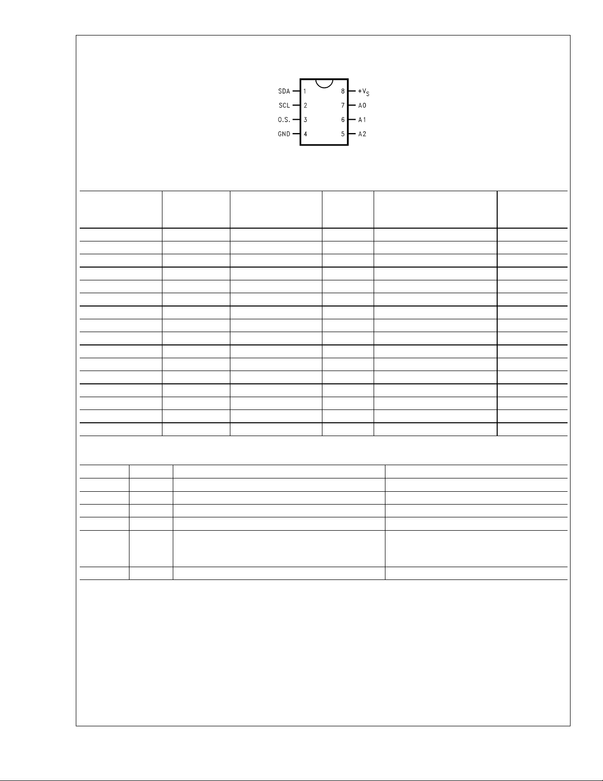
Connection Diagram
LM75
Ordering Information
SOP-8 and Mini SOP-8
01265802
Order Number
LM75BIM-3 LM75BIM-3 M08A (SOP-8) 3.3V 95 Units in Rail Yes
LM75BIMX-3 LM75BIM-3 M08A (SOP-8) 3.3V 2500 Units on Tape and Reel Yes
LM75BIMM-3 T01B MUA08A (MSOP-8) 3.3V 1000 Units on Tape and Reel Yes
LM75BIMMX-3 T01B MUA08A (MSOP-8) 3.3V 3500 Units on Tape and Reel Yes
LM75BIM-5 LM75BIM-5 M08A (SOP-8) 5V 95 Units in Rail Yes
LM75BIMX-5 LM75BIM-5 M08A (SOP-8) 5V 2500 Units on Tape and Reel Yes
LM75BIMM-5 T00B MUA08A (MSOP-8) 5V 1000 Units on Tape and Reel Yes
LM75BIMMX-5 T00B MUA08A (MSOP-8) 5V 3500 Units on Tape and Reel Yes
LM75CIM-3 LM75CIM-3 M08A (SOP-8) 3.3V 95 Units in Rail Not Available
LM75CIMX-3 LM75CIM-3 M08A (SOP-8) 3.3V 2500 Units on Tape and Reel Not Available
LM75CIMM-3 T01C MUA08A (MSOP-8) 3.3V 1000 Units on Tape and Reel Not Available
LM75CIMMX-3 T01C MUA08A (MSOP-8) 3.3V 3500 Units on Tape and Reel Not Available
LM75CIM-5 LM75CIM-5 M08A (SOP-8) 5V 95 Units in Rail Not Available
LM75CIMX-5 LM75CIM-5 M08A (SOP-8) 5V 2500 Units on Tape and Reel Not Available
LM75CIMM-5 T00C MUA08A (MSOP-8) 5V 1000 Units on Tape and Reel Not Available
LM75CIMMX-5 T00C MUA08A (MSOP-8) 5V 3500 Units on Tape and Reel Not Available
Package
Marking
NS Package
Number
Supply
Voltage
Transport Media
Noise Filter
on SDA and
SCL
Pin Description
Label Pin
SDA 1 I
SCL 2 I
O.S. 3 Overtemperature Shutdown Open Drain Output Pull– up Resistor, Controller Interrupt Line
GND 4 Power Supply Ground Ground
+V
S
A0–A2 7,6,5 User-Set I
#
2
C Serial Bi-Directional Data Line. Open Drain. From Controller, tied to a pull-up
2
C Clock Input From Controller
8 Positive Supply Voltage Input DC Voltage from 3V to 5.5V; 0.1µF bypass
2
C Address Inputs Ground (Low, “0”) or +VS(High, “1”)
Function Typical Connection
capacitor with 10µF bulk capacitance in the
near vicinity
www.national.com 2
Page 3
Pin Description (Continued)
LM75
01265803
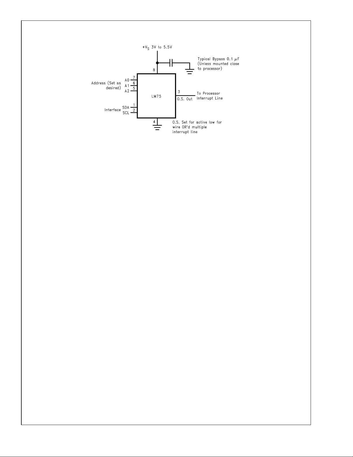
FIGURE 1. Typical Application
www.national.com3
Page 4
Absolute Maximum Ratings (Note 1)
LM75
Supply Voltage −0.3V to 6.5V
Voltage at any Pin −0.3V to +V
+ 0.3V
S
ESD Susceptibility (Note 4) LM75B LM75C
Human Body Model 2500V 1500V
Machine Model 250V 100V
Input Current at any Pin (Note 2) 5 mA
Package Input Current (Note 2) 20 mA
O.S. Output Sink Current 10 mA
O.S. Output Voltage 6.5V
Storage Temperature −65˚C to +150˚C
Operating Ratings
Specified Temperature Range T
(Note 5) −55˚C to +125˚C
Supply Voltage Range (+V
) +3.0V to +5.5V
S
MIN
Soldering Information, Lead Temperature
SOP and MSOP Package (Note 3)
Vapor Phase (60 seconds)
Infrared (15 seconds)
215˚C
220˚C
Temperature-to-Digital Converter Characteristics
Unless otherwise noted, these specifications apply for +VS= +5 Vdc for LM75BIM-5, LM75BIMM-5, LM75CIM-5, and
LM75CIMM-5 and +V
apply for T
A=TJ=TMIN
Parameter Conditions
Accuracy T
Resolution 9 Bits
Temperature Conversion Time (Note 8) 100 ms
Quiescent Current LM75B I
O.S. Output Saturation Voltage I
O.S. Delay (Note 10) 1 Conversions (min)
T
Default Temperature (Note 11) 80 ˚C
OS
T
Default Temperature (Note 11) 75 ˚C
HYST
= +3.3 Vdc for LM75BIM-3, LM75BIMM-3, LM75CIM-3, and LM75CIMM-3 (Note 6). Boldface limits
S
to T
LM75C I
; all other limits TA=TJ= +25˚C, unless otherwise noted.
MAX
Typical
(Note 12)
= −25˚C to +100˚C
A
T
= −55˚C to +125˚C
A
2
C Inactive 0.25 0.5 mA (max)
Shutdown Mode, +V
Shutdown Mode, +V
2
C Inactive 0.25 1.0 mA (max)
Shutdown Mode, +V
Shutdown Mode, +V
= 4.0 mA 0.8 V (max)
OUT
=3V 4 µA
S
=5V 6 µA
S
=3V 4 µA
S
=5V 6 µA
S
Limits
(Note 7)
±
2.0 ˚C (max)
±
3.0 ˚C (max)
Units
(Limit)
(Note 9)
6 Conversions (max)
to T
MAX
Logic Electrical Characteristics
DIGITAL DC CHARACTERISTICS Unless otherwise noted, these specifications apply for +VS= +5 Vdc for LM75BIM-5,
LM75BIMM-5, LM75CIM-5, and LM75CIMM-5 and +V
LM75CIMM-3 (Note 6). Boldface limits apply for T
noted.
Symbol Parameter Conditions
V
IN(1)
V
IN(0)
I
IN(1)
I
IN(0)
C
IN
I
OH
V
OL
www.national.com 4
Logical “1” Input Voltage +VSx 0.7 V (min)
Logical “0” Input Voltage −0.3 V (min)
Logical “1” Input Current VIN= 5V 0.005 1.0 µA (max)
Logical “0” Input Current VIN= 0V −0.005 −1.0 µA (max)
All Digital Inputs 20 pF
High Level Output Current VOH=5V 100 µA (max)
Low Level Output Voltage IOL=3mA 0.4 V (max)
= +3.3 Vdc for LM75BIM-3, LM75BIMM-3, LM75CIM-3, and
S
A=TJ=TMIN
to T
; all other limits TA=TJ= +25˚C, unless otherwise
MAX
Typical
(Note 12)
Limits
(Note 7)
+V
+ 0.5 V (max)
S
+V
x 0.3 V (max)
S
Units
(Limit)
Page 5
Logic Electrical Characteristics (Continued)
DIGITAL DC CHARACTERISTICS Unless otherwise noted, these specifications apply for +VS= +5 Vdc for LM75BIM-5,
LM75BIMM-5, LM75CIM-5, and LM75CIMM-5 and +V
LM75CIMM-3 (Note 6). Boldface limits apply for T
noted.
Symbol Parameter Conditions
t
OF
Output Fall Time CL= 400 pF 250 ns (max)
I2C DIGITAL SWITCHING CHARACTERISTICS Unless otherwise noted, these specifications apply for +VS= +5 Vdc for
LM75BIM-5, LM75BIMM-5, LM75CIM-5, and LM75CIMM-5 and +V
and LM75CIMM-3. C
T
J=TMIN
to T
(load capacitance) on output lines = 80 pF unless otherwise specified. Boldface limits apply for TA=
L
; all other limits TA=TJ= +25˚C, unless otherwise noted. The switching characteristics of the LM75 fully
MAX
meet or exceed the published specifications of the I
and SDA signals related to the LM75. They are not the I
Symbol Parameter Conditions
t
1
t
2
t
3
t
4
t
5
t
TIMEOUT
SCL (Clock) Period 2.5 µs (min)
Data in Set-Up Time to SCL High 100 ns (min)
Data Out Stable after SCL Low 0 ns (min)
SDA Low Set-Up Time to SCL Low (Start Condition) 100 ns (min)
SDA High Hold Time after SCL High (Stop Condition) 100 ns (min)
SDA Time Low for Reset of Serial Interface (Note 13) LM75B 75
= +3.3 Vdc for LM75BIM-3, LM75BIMM-3, LM75CIM-3, and
S
A=TJ=TMIN
I
=3mA
O
2
C bus. The following parameters are the timing relationships between SCL
2
C bus specifications.
to T
S
; all other limits TA=TJ= +25˚C, unless otherwise
MAX
Typical
(Note 12)
Limits
(Note 7)
= +3.3 Vdc for LM75BIM-3, LM75BIMM-3, LM75CIM-3,
Typical
(Note 12)
Limits
(Note 7)
325
LM75C Not
Applicable
LM75
Units
(Limit)
Units
(Limit)
ms (min)
ms (max)
01265804
Note 1: Absolute Maximum Ratings indicate limits beyond which damage to the device may occur. DC and AC electrical specifications do not apply when operating
the device beyond its rated operating conditions.
Note 2: When the input voltage (V
maximum package input current rating limits the number of pins that can safely exceedthe power supplies with an input current of 5 mA to four.
Note 3: See AN-450 “Surface Mounting Methods and Their Effect on Product Reliability” or the section titled “Surface Mount” found in a current National
Semiconductor Linear Data Book for other methods of soldering surface mount devices.
Note 4: Human body model, 100 pF discharged through a 1.5 kΩ resistor. Machine model, 200 pF discharged directly into each pin.
) at any pin exceeds the power supplies (V
I
<
I
GND or V
>
+VS) the current at that pin should be limited to 5 mA. The 20 mA
I
www.national.com5
Page 6
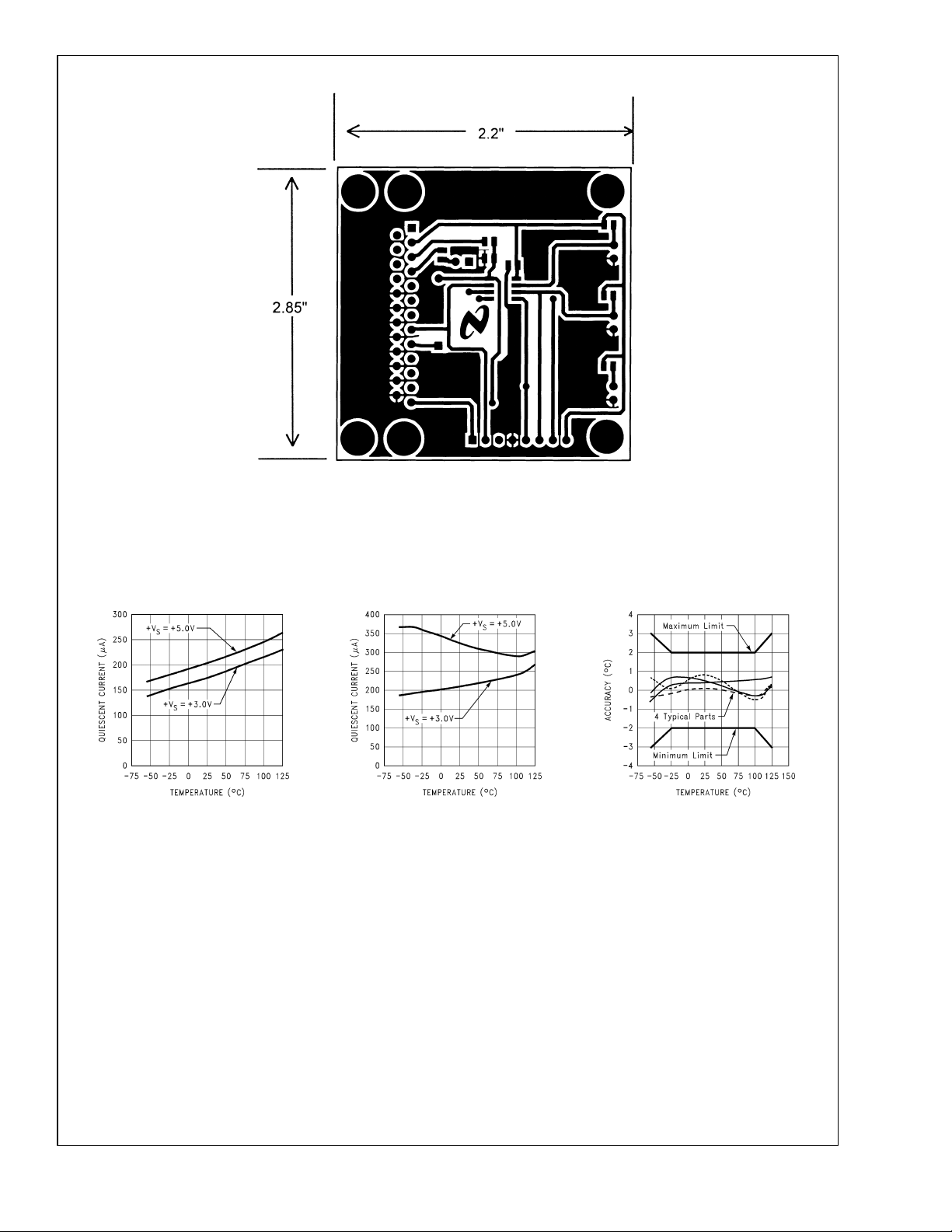
Note 5: LM75 θJA(thermal resistance, junction-to-ambient) when attached to a printed circuit board with 2 oz. foil similar to the one shown in Figure 3 is summarized
in the table below:
LM75
Device Number
NS Package
Number
Thermal
Resistance (θ
)
JA
LM75BIM-3, LM75BIM-5, LM75CIM-3, LM75CIM-5 M08A 200˚C/W
LM75BIMM-3, LM75BIMM-5, LM75CIMM-3, LM75CIMM-5 MUA08A 250˚C/W
Note 6: All part numbers of the LM75 will operate properly over the +VSsupply voltage range of 3V to 5.5V. The devices are tested and specified for rated accuracy
at their nominal supply voltage. Accuracy will typically degrade 1˚C/V of variation in +V
Note 7: Limits are guaranteed to National’s AOQL (Average Outgoing Quality Level).
Note 8: This specification is provided only to indicate how often temperature data is updated. The LM75 can be read at any time without regard to conversion state
(and will yield last conversion result). If a conversion is in process it will be interrupted and restarted after the end of the read.
Note 9: For best accuracy, minimize output loading. Higher sink currents can affect sensor accuracy with internal heating. This can cause an error of 0.64˚C at full
rated sink current and saturation voltage based on junction-to-ambient thermal resistance.
Note 10: O.S. Delay is user programmable up to 6 “over limit” conversions before O.S. is set to minimize false tripping in noisy environments.
Note 11: Default values set at power up.
Note 12: Typicals are at T
Note 13: Holding the SDA line low for a time greater than t
High).
= 25˚C and represent most likely parametric norm.
A
will cause the LM75B to reset SDA to the IDLE state of the serial bus communication (SDA set
TIMEOUT
as it varies from the nominal value.
S
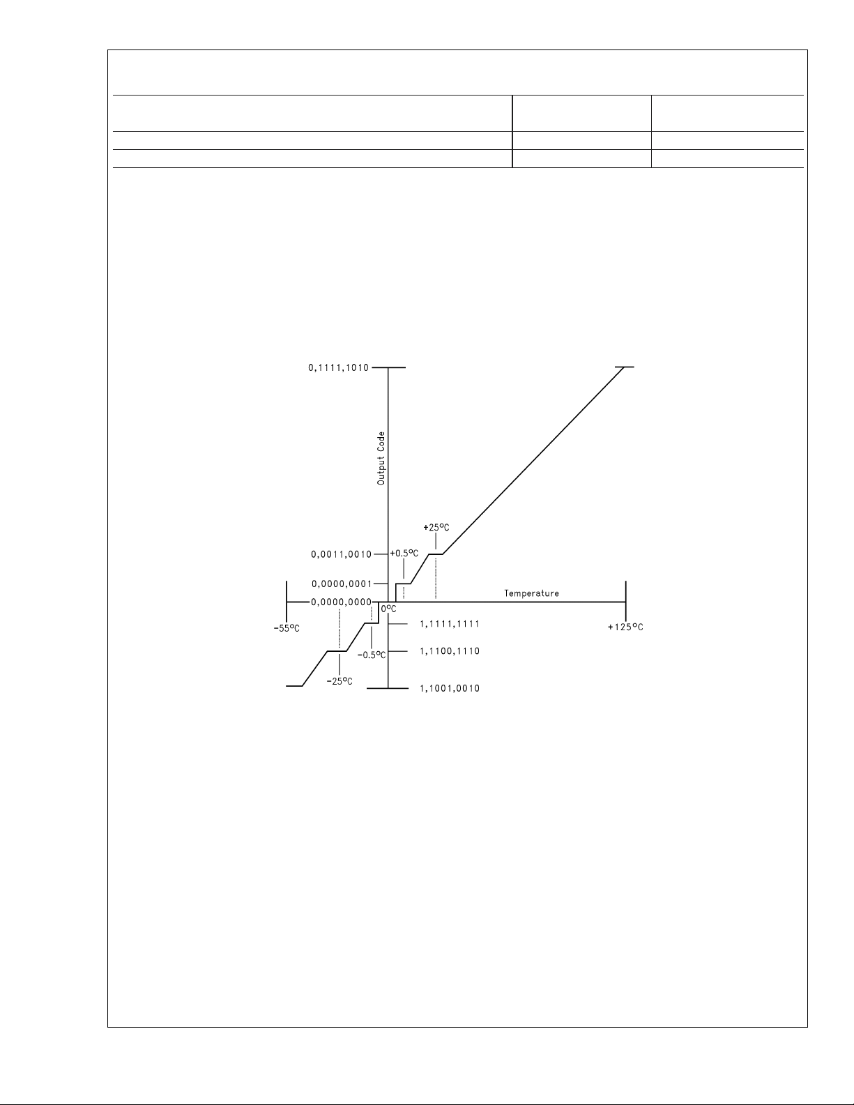
FIGURE 2. Temperature-to-Digital Transfer Function (Non-linear scale for clarity)
www.national.com 6
01265805
Page 7
01265806
LM75
FIGURE 3. Printed Circuit Board Used for Thermal Resistance Specifications
Typical Performance Characteristics
Static Quiescent Current vs
Temperature
01265816
Dynamic Quiescent Current vs
Temperature Accuracy vs Temperature
1.0 Functional Description
The LM75 temperature sensor incorporates a band-gap type
temperature sensor and 9-bit ADC (Delta-Sigma
Analog-to-Digital Converter). The temperature data output of
the LM75 is available at all times via the I
conversion is in progress, it will be stopped and restarted
after the read. A digital comparator is also incorporated that
compares a series of readings, the number of which is
user-selectable, to user-programmable setpoint and hysteresis values. The comparator trips the O.S. output line, which
is programmable for mode and polarity.
The LM75B contains all the functionality of the LM75C, plus
two additional features:
1. The LM75B has an integrated low-pass filter on both the
SDA and the SCL line. These filters increase communications reliability in noisy environments.
2
C bus. If a
01265817 01265818
2. The LM75B also has a bus fault timeout feature. If the
SDA line is held low for longer than t
TIMEOUT
(75 ms
minimum to 325 ms maximum) the LM75B will reset to
the IDLE state (SDA set to high impedance) and wait for
a new start condition.
1.1 O.S. OUTPUT, T
OS
AND T
HYST
LIMITS
In Comparator mode the O.S. Output behaves like a thermostat. The output becomes active when temperature exceeds the T
temperature drops below the T
limit, and leaves the active state when the
OS
limit. In this mode the
HYST
O.S. output can be used to turn a cooling fan on, initiate an
emergency system shutdown, or reduce system clock
speed. Shutdown mode does not reset O.S. state in a comparator mode.
In Interrupt mode exceeding T
O.S. will remain active indefinitely until reset by reading any
register via the I
2
C interface. Once O.S. has been activated
also makes O.S. active but
OS
www.national.com7
Page 8

1.0 Functional Description (Continued)
LM75
by crossing T
Temperature going below T
, then reset, it can be activated again only by
OS
. Again, it will remain active
HYST
indefinitely until being reset by a read. Placing the LM75 in
shutdown mode also resets the O.S. Output.
1.2 POWER UP AND POWER DOWN
The LM75 always powers up in a known state. The power up
default conditions are:
1. Comparator mode
OS
HYST
= 80˚C
= 75˚C
2. T
3. T
4. O.S. active low
5. Pointer = “00”
2
If the LM75 is not connected to the I
C bus on power up, it
will act as a stand-alone thermostat with the above temperature settings.
When the supply voltage is less than about 1.7V, the LM75 is
considered powered down. As the supply voltage rises
above the nominal 1.7V power up threshold, the internal
registers are reset to the power up default values listed
above.
2
C BUS INTERFACE
1.3 I
The LM75 operates as a slave on the I
line is an input (no clock is generated by the LM75) and the
SDA line is a bi-directional serial data path. According to I
2
C bus, so the SCL
2
bus specifications, the LM75 has a 7-bit slave address. The
four most significant bits of the slave address are hard wired
inside the LM75 and are “1001”. The three least significant
bits of the address are assigned to pins A2– A0, and are set
by connecting these pins to ground for a low, (0); or to +V
for a high, (1).
Therefore, the complete slave address is:
1 0 0 1 A2 A1 A0
MSB LSB
C
S
Note 14: These interrupt mode resets of O.S. occur only when LM75 is read or placed in shutdown. Otherwise, O.S. would remain active indefinitely for any event.
01265807
FIGURE 4. O.S. Output Temperature Response Diagram
www.national.com 8
Page 9

1.0 Functional Description (Continued)
1.4 TEMPERATURE DATA FORMAT
Temperature data can be read from the Temperature, T
Set Point, and T
Set Point, and T
T
OS
Set Point registers; and written to the
HYST
Set Point registers. Temperature
HYST
data is represented by a 9-bit, two’s complement word with
an LSB (Least Significant Bit) equal to 0.5˚C:
Temperature Digital Output
Binary Hex
+125˚C 0 1111 1010 0FAh
+25˚C 0 0011 0010 032h
+0.5˚C 0 0000 0001 001h
0˚C 0 0000 0000 000h
−0.5˚C 1 1111 1111 1FFh
−25˚C 1 1100 1110 1CEh
−55˚C 1 1001 0010 192h
OS
LM75
1.7 COMPARATOR/INTERRUPT MODE
As indicated in the O.S. Output Temperature Response Diagram, Figure 4, the events that trigger O.S. are identical for
either Comparator or Interrupt mode. The most important
difference is that in Interrupt mode the O.S. will remain set
indefinitely once it has been set. To reset O.S. while in
Interrupt mode, perform a read from any register in the
LM75.
1.8 O.S. OUTPUT
The O.S. output is an open-drain output and does not have
an internal pull-up. A “high” level will not be observed on this
pin until pull-up current is provided from some external
source, typically a pull-up resistor. Choice of resistor value
depends on many system factors but, in general, the pull-up
resistor should be as large as possible. This will minimize
any errors due to internal heating of the LM75. The maximum resistance of the pull up, based on LM75 specification
for High Level Output Current, to provide a 2V high level, is
30 kΩ.
1.5 SHUTDOWN MODE
Shutdown mode is enabled by setting the shutdown bit in the
Configuration register via the I
2
C bus. Shutdown mode reduces power supply current to 4 µA typical. In Interrupt mode
O.S. is reset if previously set and is undefined in Comparator
mode during shutdown. The I
Activity on the clock and data lines of the I
slightly increase shutdown mode quiescent current. T
, and Configuration registers can be read from and
T
HYST
2
C interface remains active.
2
C bus may
OS
written to in shutdown mode.
1.6 FAULT QUEUE
A fault queue of up to 6 faults is provided to prevent false
tripping of O.S. when the LM75 is used in noisy environments. The number of faults set in the queue must occur
consecutively to set the O.S. output.
1.9 O.S. POLARITY
The O.S. output can be programmed via the configuration
register to be either active low (default mode), or active high.
In active low mode the O.S. output goes low when triggered
exactly as shown on the O.S. Output Temperature Response
Diagram, Figure 4. Active high simply inverts the polarity of
the O.S. output.
,
www.national.com9
Page 10

1.0 Functional Description (Continued)
LM75
1.10 INTERNAL REGISTER STRUCTURE
01265808
There are four data registers in the LM75, selected by the
Pointer register. At power-up the Pointer is set to “00”; the
location for the Temperature Register. The Pointer register
latches whatever the last location it was set to. In Interrupt
Mode, a read from the LM75, or placing the device in shutdown mode, resets the O.S. output. All registers are read
and write, except the Temperature register which is read
only.
A write to the LM75 will always include the address byte and
the Pointer byte. A write to the Configuration register requires one data byte, and the T
OS
and T
HYST
registers
require two data bytes.
Reading the LM75 can take place either of two ways: If the
location latched in the Pointer is correct (most of the time it is
expected that the Pointer will point to the Temperature register because it will be the data most frequently read from the
LM75), then the read can simply consist of an address byte,
followed by retrieving the corresponding number of data
bytes. If the Pointer needs to be set, then an address byte,
pointer byte, repeat start, and another address byte will
accomplish a read.
The first data byte is the most significant byte with most
significant bit first, permitting only as much data as necessary to be read to determine temperature condition. For
instance, if the first four bits of the temperature data indicates an overtemperature condition, the host processor
could immediately take action to remedy the excessive temperatures. At the end of a read, the LM75 can accept either
Acknowledge or No Acknowledge from the Master (No Acknowledge is typically used as a signal for the slave that the
Master has read its last byte).
An inadvertent 8-bit read from a 16-bit register, with the D7
bit low, can cause the LM75 to stop in a state where the SDA
line is held low as shown in Figure 5. This can prevent any
further bus communication until at least 9 additional clock
cycles have occurred. Alternatively, the master can issue
clock cycles until SDA goes high, at which time issuing a
“Stop” condition will reset the LM75.
FIGURE 5. Inadvertent 8-Bit Read from 16-Bit Register where D7 is Zero (“0”)
www.national.com 10
01265809
Page 11
1.0 Functional Description (Continued)
1.11 POINTER REGISTER
(Selects which registers will be read from or written to):
P7 P6 P5 P4 P3 P2 P1 P0
000000Register
Select
P0-P1: Register Select:
P1 P0 Register
0 0 Temperature (Read only) (Power-up default)
0 1 Configuration (Read/Write)
10T
11T
P2–P7: Must be kept zero. 1.12 TEMPERATURE REGISTER
(Read Only):
D15 D14 D13 D12 D11 D10 D9 D8 D7 D6 D5 D4 D3 D2 D1 D0
MSBBit7Bit6Bit5Bit4Bit3Bit2Bit1LSBXXXXXXX
(Read/Write)
HYST
(Read/Write)
OS
LM75
D0–D6: Undefined
1.13 CONFIGURATION REGISTER
D7–D15: Temperature Data. One LSB = 0.5˚C. Two’s
complement format.
(Read/Write):
D7 D6 D5 D4 D3 D2 D1 D0
0 0 0 Fault Queue O.S. Cmp/Int Shutdown
Polarity
Power up default is with all bits “0” (zero).
D0: Shutdown: When set to 1 the LM75 goes to low power
shutdown mode.
D1: Comparator/Interrupt mode: 0 is Comparator mode, 1 is
D3–D4: Fault Queue: Number of faults necessary to detect
before setting O.S. output to avoid false tripping due to
noise. Faults are determind at the end of a conversion.
Conversions take about 100 ms, typically, to complete.
Interrupt mode.
D2: O.S. Polarity: 0 is active low, 1 is active high. O.S. is an
open-drain output under all conditions.
D4 D3 Number of Faults
0 0 1 (Power-up default)
012
104
116
D5–D7: These bits are used for production testing and must
1.14 T
AND TOSREGISTER
HYST
be kept zero for normal operation.
(Read/Write):
D15 D14 D13 D12 D11 D10 D9 D8 D7 D6 D5 D4 D3 D2 D1 D0
MSBBit7Bit6Bit5Bit4Bit3Bit2Bit1LSBXXXXXXX
D0–D6: Undefined
D7–D15: T
default is T
HYST
= 80˚C, T
OS
Or TOSTrip Temperature Data. Power up
= 75˚C.
HYST
www.national.com11
Page 12

LM75
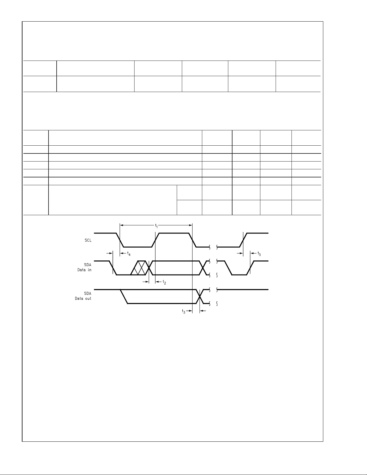
C Timing Diagrams
2
2.0 I
FIGURE 6. Timing Diagram
01265810
www.national.com 12
Page 13

LM75
C Timing Diagrams (Continued)
2
2.0 I
01265811
FIGURE 7. Timing Diagrams (Continued)
www.national.com13
Page 14

3.0 Application Hints
LM75
To get the expected results when measuring temperature
with an integrated circuit temperature sensor like the LM75,
it is important to understand that the sensor measures its
own die temperature. For the LM75, the best thermal path
between the die and the outside world is through the LM75’s
pins. In the MSOP-8 package, the GND pin is directly connected to the die, so the GND pin provides the best thermal
path. If the other pins are at different temperatures (unlikely,
but possible), they will affect the die temperature, but not as
strongly as the GND pin. In the SO-8 package, none of the
pins is directly connected to the die, so they will all contribute
similarly to the die temperature. Because the pins represent
a good thermal path to the LM75 die, the LM75 will provide
an accurate measurement of the temperature of the printed
circuit board on which it is mounted. There is a less efficient
thermal path between the plastic package and the LM75 die.
If the ambient air temperature is significantly different from
the printed circuit board temperature, it will have a small
effect on the measured temperature.
In probe-type applications, the LM75 can be mounted inside
a sealed-end metal tube, and can then be dipped into a bath
or screwed into a threaded hole in a tank. As with any IC, the
LM75 and accompanying wiring and circuits must be kept
insulated and dry, to avoid leakage and corrosion. This is
especially true if the circuit may operate at cold temperatures
where condensation can occur. Printed-circuit coatings and
varnishes such as Humiseal and epoxy paints or dips are
often used to insure that moisture cannot corrode the LM75
or its connections.
Digital Noise Issues
The LM75B features an integrated low-pass filter on both the
SCL and the SDA digital lines to mitigate the effects of bus
noise. Although this filtering makes the LM75B communication robust in noisy environments, good layout practices are
always recommended. Minimize noise coupling by keeping
digital traces away from switching power supplies. Also,
ensure that digital lines containing high-speed data communications cross at right angles to the SDA and SCL lines.
Excessive noise coupling into the SDA and SCL lines on the
LM75C — specifically noise with amplitude greater than 400
(the LM75’s typical hysteresis), overshoot greater than
mV
pp
300 mV above +V
, and undershoot more than 300 mV
s
below GND — may prevent successful serial communication
with the LM75C. Serial bus no-acknowledge is the most
common symptom, causing unnecessary traffic on the bus.
The layout procedures mentioned above apply also to the
LM75C. Although the serial bus maximum frequency of communication is only 100 kHz, care must be taken to ensure
proper termination within a system with long printed circuit
board traces or multiple parts on the bus. Resistance can be
added in series with the SDA and SCL lines to further help
filter noise and ringing. A 5 kΩ resistor should be placed in
series with the SCL line, placed as close as possible to the
SCL pin on the LM75C. This 5 kΩ resistor, with the 5 pF to 10
pF stray capacitance of the LM75 provides a 6 MHz to 12
MHz low pass filter, which is sufficient filtering in most cases.
4.0 Typical Applications
When using the two-wire interface: program O.S. for active high and connect O.S. directly to Q2’s gate.
FIGURE 8. Simple Fan Controller, Interface Optional
01265812
www.national.com 14
Page 15
4.0 Typical Applications (Continued)
LM75
01265813
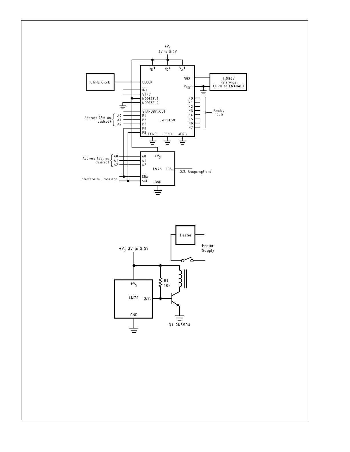
FIGURE 9. Data Acquisition System with Temperature Input via I2C Bus
01265814
FIGURE 10. Simple Thermostat, Interface Optional
www.national.com15
Page 16
4.0 Typical Applications (Continued)
LM75
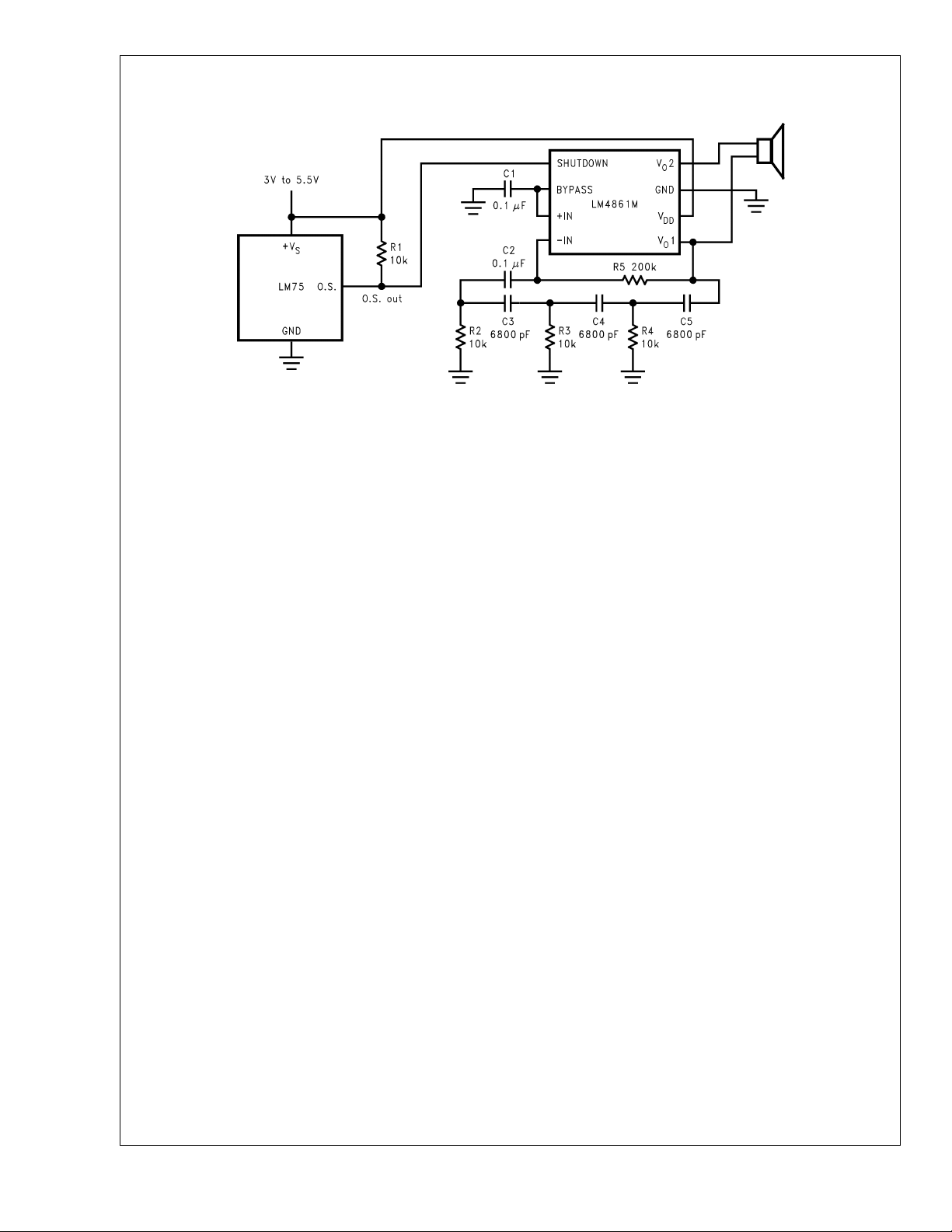
FIGURE 11. Temperature Sensor with Loudmouth Alarm (Barking Watchdog)
01265815
www.national.com 16
Page 17

Physical Dimensions inches (millimeters) unless otherwise noted
LM75
8-Lead (0.150" Wide) Molded Small Outline Package (SOP), JEDEC
Order Number LM75CIM-3, LM75CIMX-3, LM75CIM-5, LM75CIMX-5,
LM75BIM-3, LM75BIMX-3, LM75BIM-5, or LM75BIMX-5
NS Package Number M08A
www.national.com17
Page 18
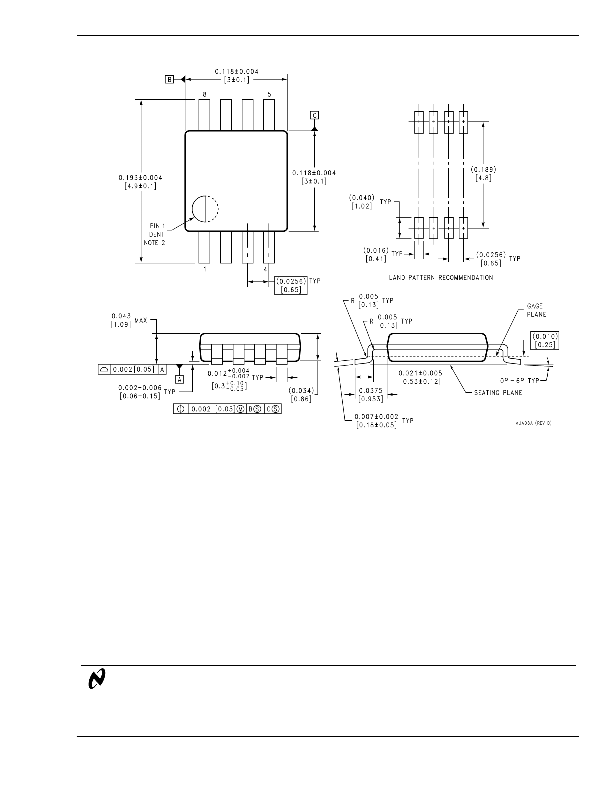
Physical Dimensions inches (millimeters) unless otherwise noted (Continued)
8-Lead Molded Mini Small Outline Package (MSOP)
(JEDEC REGISTRATION NUMBER M0-187)
Order Number LM75CIMM-3, LM75CIMMX-3,
LM75CIMM-5, LM75CIMMX-5,
LM75BIMM-3, LM75BIMMX-3,
LM75BIMM-5, or LM75BIMMX-5
NS Package Number MUA08A
LIFE SUPPORT POLICY
NATIONAL’S PRODUCTS ARE NOT AUTHORIZED FOR USE AS CRITICAL COMPONENTS IN LIFE SUPPORT
DEVICES OR SYSTEMS WITHOUT THE EXPRESS WRITTEN APPROVAL OF THE PRESIDENT AND GENERAL
COUNSEL OF NATIONAL SEMICONDUCTOR CORPORATION. As used herein:
1. Life support devices or systems are devices or
systems which, (a) are intended for surgical implant
LM75 Digital Temperature Sensor and Thermal Watchdog with Two-Wire Interface
into the body, or (b) support or sustain life, and
whose failure to perform when properly used in
accordance with instructions for use provided in the
2. A critical component is any component of a life
support device or system whose failure to perform
can be reasonably expected to cause the failure of
the life support device or system, or to affect its
safety or effectiveness.
labeling, can be reasonably expected to result in a
significant injury to the user.
National Semiconductor
Corporation
Americas
Email: support@nsc.com
www.national.com
National Semiconductor
Europe
Fax: +49 (0) 180-530 85 86
Email: europe.support@nsc.com
Deutsch Tel: +49 (0) 69 9508 6208
English Tel: +44 (0) 870 24 0 2171
Français Tel: +33 (0) 1 41 91 8790
National Semiconductor
Asia Pacific Customer
Response Group
Tel: 65-2544466
Fax: 65-2504466
Email: ap.support@nsc.com
National Semiconductor
Japan Ltd.
Tel: 81-3-5639-7560
Fax: 81-3-5639-7507
National does not assume any responsibility for use of any circuitry described, no circuit patent licenses are implied and National reserves the right at any time without notice to change said circuitry and specifications.
 Loading...