

Page 1
LM134/LM234/LM334
3-Terminal Adjustable Current Sources
General Description
The LM134/LM234/LM334 are 3-terminal adjustable current
sources featuring 10,000:1 range in operating current, excellent current regulation and a wide dynamic voltage range of
1V to 40V. Current is established with one external resistor
and no other parts are required. Initial current accuracy is
±
3%. The LM134/LM234/LM334 are true floating current
sources with no separate power supply connections. In addition, reverse applied voltages of up to 20V will draw only a
few dozen microamperes of current, allowing the devices to
act as both a rectifier and current source in AC applications.
The sense voltage used to establish operating current in the
LM134 is 64mV at 25˚C and is directly proportional to absolute temperature (˚K). The simplest one external resistor
connection, then, generates a current with ≈+0.33%/˚C temperature dependence. Zero drift operation can be obtained
by adding one extra resistor and a diode.
Applications for the current sources include bias networks,
surge protection, low power reference, ramp generation,
LED driver, and temperature sensing. The LM234-3 and
LM234-6 are specified as true temperature sensors with
guaranteed initial accuracy of
These devices are ideal in remote sense applications because series resistance in long wire runs does not affect
accuracy. In addition, only 2 wires are required.
The LM134 is guaranteed over a temperature range of
−55˚C to +125˚C, the LM234 from −25˚C to +100˚C and the
LM334 from 0˚C to +70˚C. These devices are available in
TO-46 hermetic, TO-92 and SO-8 plastic packages.
Features
n Operates from 1V to 40V
n 0.02%/V current regulation
n Programmable from 1µA to 10mA
n True 2-terminal operation
n Available as fully specified temperature sensor
±
n
3% initial accuracy
March 2000
±
3˚C and±6˚C, respectively.
LM134/LM234/LM334 3-Terminal Adjustable Current Sources
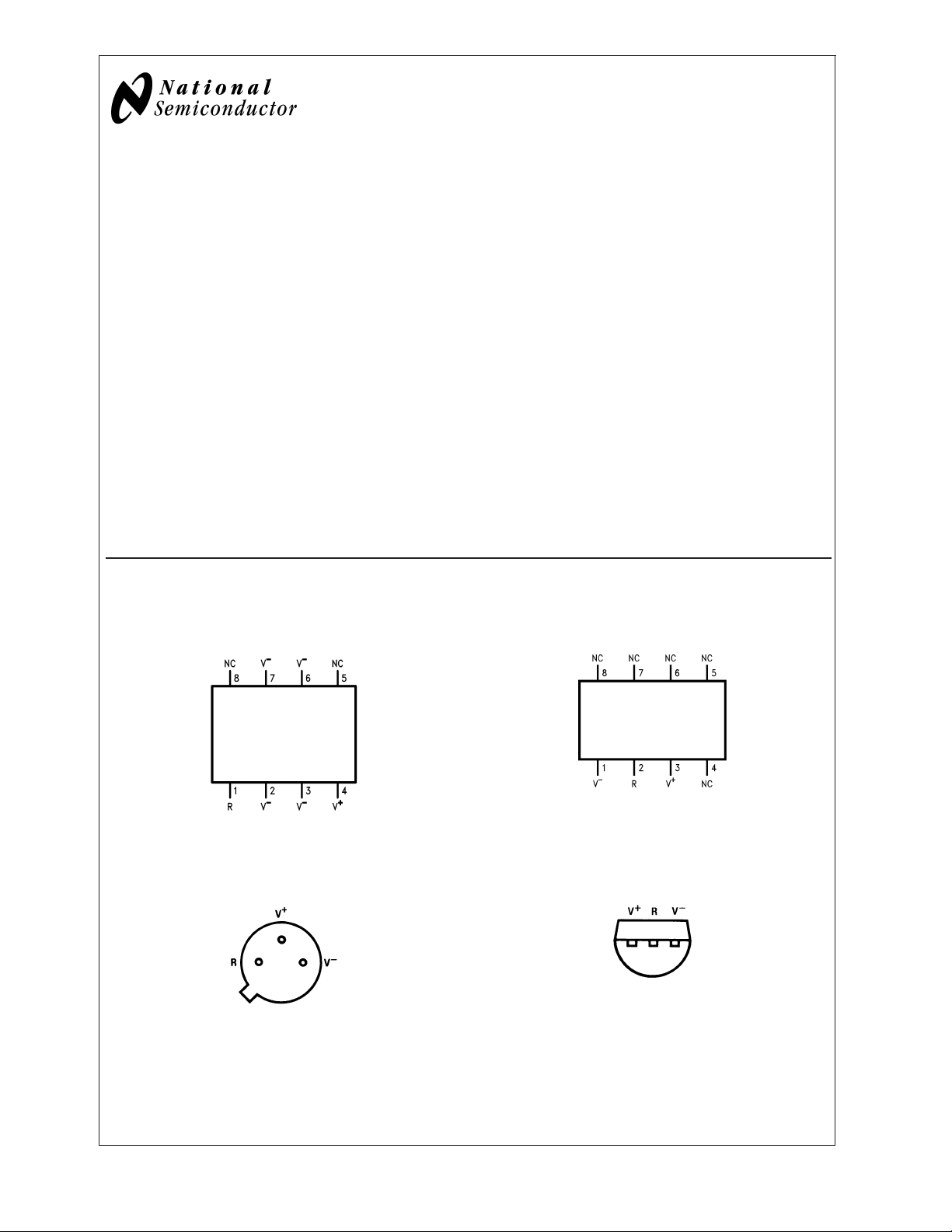
Connection Diagrams
SO-8
Surface Mount Package
Order Number LM334M or LM334MX
See NS Package Number M08A
TO-46
Metal Can Package TO-92 Plastic Package
00569712
V−Pin is electrically connected to case.
Bottom View
Order Number LM134H,
LM234H or LM334H
See NS Package
Number H03H
00569724
SO-8 Alternative Pinout
Surface Mount Package
00569725
Order Number LM334SM or LM334SMX
See NS Package Number M08A
00569710
Bottom View
Order Number LM334Z, LM234Z-3 or LM234Z-6
See NS Package Number Z03A
© 2004 National Semiconductor Corporation DS005697 www.national.com
Page 2
Absolute Maximum Ratings (Note 1)
If Military/Aerospace specified devices are required,
please contact the National Semiconductor Sales Office/
Distributors for availability and specifications.
+
to V−Forward Voltage
V
LM134/LM234/LM334 40V
LM134/LM234/LM334
LM234-3/LM234-6 30V
+
V
to V−Reverse Voltage 20V
R Pin to V
−
Voltage 5V
Set Current 10 mA
Power Dissipation 400 mW
LM234/LM234-3/LM234-6 −25˚C to +100˚C
LM334 0˚C to +70˚C
Soldering Information
TO-92 Package (10 sec.) 260˚C
TO-46 Package (10 sec.) 300˚C
SO Package
Vapor Phase (60 sec.) 215˚C
Infrared (15 sec.) 220˚C
See AN-450 “Surface Mounting Methods and Their Effect on
Product Reliability” (Appendix D) for other methods of soldering surface mount devices.
ESD Susceptibility (Note 6) 2000V
Operating Temperature Range (Note
5)
LM134 −55˚C to +125˚C
Electrical Characteristics (Note 2)
Parameter Conditions LM134/LM234 LM334 Units
Set Current Error, V
(Note 3) 1mA
Ratio of Set Current to 100µA ≤ I
Bias Current 1mA ≤ I
Minimum Operating Voltage 2µA ≤ I
Average Change in Set Current 2µA ≤ I
with Input Voltage 1.5 ≤ V
+
=2.5V, 10µA ≤ I
2µA ≤ I
2µA≤I
100µA
1mA
5V ≤ V
1mA
≤ 1mA 3 6 %
SET
<
I
≤ 5mA 5 8 %
SET
<
10µA 8 12 %
SET
≤ 1mA 14 18 23 14 18 26
SET
≤ 5mA 14 14
SET
≤100 µA 18 23 18 26
SET
≤ 100µA 0.8 0.8 V
SET
<
I
≤ 1mA 0.9 0.9 V
SET
<
I
≤ 5mA 1.0 1.0 V
SET
≤ 1mA
SET
+
≤ 5V 0.02 0.05 0.02 0.1 %/V
+
≤ 40V 0.01 0.03 0.01 0.05 %/V
<
I
≤ 5mA
SET
1.5V ≤ V ≤ 5V 0.03 0.03 %/V
5V ≤ V ≤ 40V 0.02 0.02 %/V
Temperature Dependence of 25µA ≤ I
≤ 1mA 0.96T T 1.04T 0.96T T 1.04T
SET
Set Current (Note 4)
Effective Shunt Capacitance 15 15 pF
Note 1: .“Absolute Maximum Ratings” indicate limits beyond which damage to the device may occur. Operating Ratings indicate conditions for which the device is
functional, but do not guarantee specific performance limits.
Note 2: Unless otherwise specified, tests are performed at T
Note 3: Set current is the current flowing into the V
determined by the following formula: I
0.336%/˚C
@
Tj= 25˚C (227 µV/˚C).
= 67.7 mV/R
SET
= 25˚C with pulse testing so that junction temperature does not change during test
j
+
pin. For the Basic 2-Terminal Current Source circuit shown on the first page of this data sheet. I
(@25˚C). Set current error is expressed as a percent deviation from this amount. I
SET
Min Typ Max Min Typ Max
SET
SET
increases at
is
www.national.com 2
Page 3
Electrical Characteristics (Note 2) (Continued)
Note 4: I
(˚K).
Note 5: For elevated temperature operation, T
Note 6: Human body model, 100pF discharged through a 1.5kΩ resistor.
is directly proportional to absolute temperature (˚K). I
SET
max is:
J
Thermal Resistance TO-92 TO-46 SO-8
θ
(Junction to
ja
Ambient)
(Junction to Case) N/A 32˚C/W 80˚C/W
θ
jc
at any temperature can be calculated from: I
SET
SET=Io
LM134 150˚C
LM234 125˚C
LM334 100˚C
180˚C/W (0.4" leads) 440˚C/W 165˚C/W
160˚C/W (0.125"
leads)
(T/To) where Iois I
measured at T
SET
Electrical Characteristics (Note 2)
Parameter Conditions LM234-3 LM234-6 Units
Set Current Error, V
(Note 3) T
+
=2.5V, 100µA ≤ I
= 25˚
J
SET
≤ 1mA
Equivalent Temperature Error
Ratio of Set Current to 100µA ≤ I
≤ 1mA 14 18 26 14 18 26
SET
Bias Current
Minimum Operating Voltage 100µA I
Average Change in Set Current 100µA ≤ I
with Input Voltage 1.5 ≤ V
5V ≤ V
Temperature Dependence of 100µA ≤ I
≤ 1mA 0.9 0.9 V
SET
≤ 1mA
SET
+
≤ 5V 0.02 0.05 0.02 0.01 %/V
+
≤ 30V 0.01 0.03 0.01 0.05 %/V
≤ 1mA 0.98T T 1.02T 0.97T T 1.03T
SET
Set Current (Note 4) and
Equivalent Slope Error
Effective Shunt Capacitance 15 15 pF
Min Typ Max Min Typ Max
±
1
±
3
±
2
±
±
±
2%
6˚C
3%
LM134/LM234/LM334
o
www.national.com3
Page 4
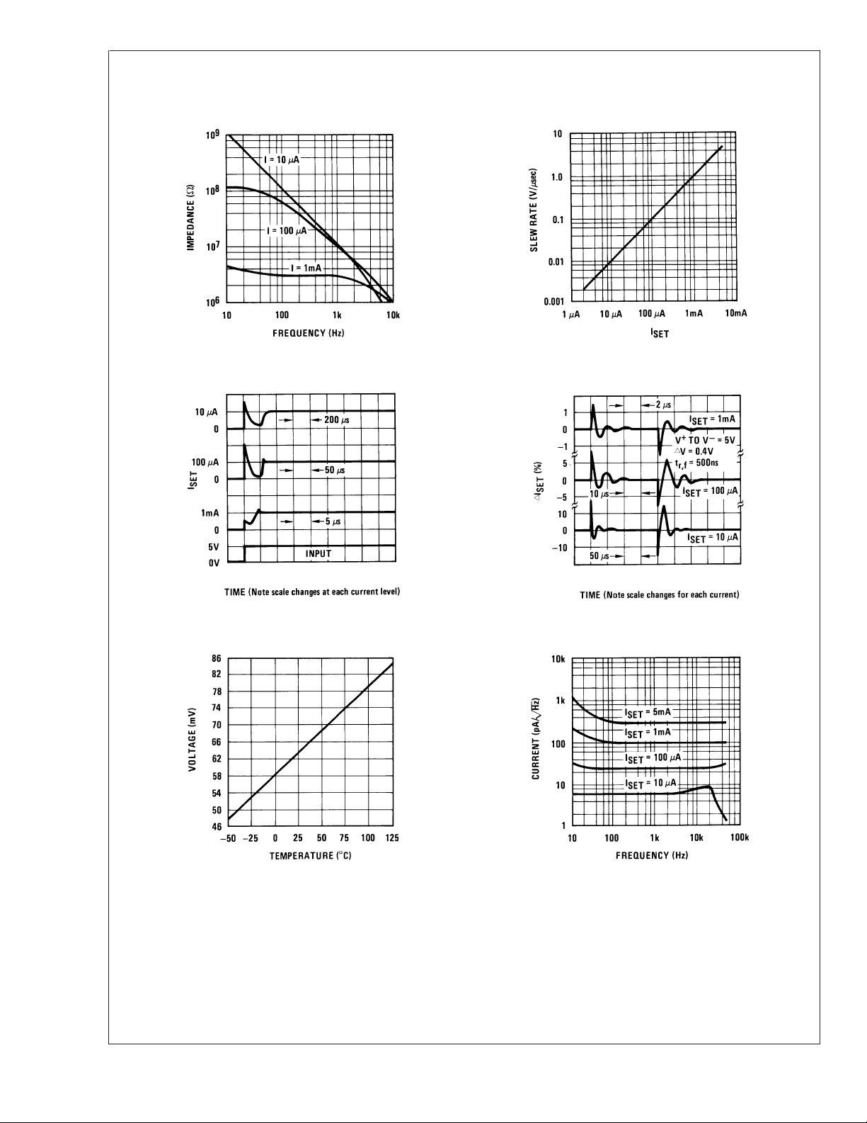
Typical Performance Characteristics
Output Impedance
LM134/LM234/LM334
00569730 00569731
Start-Up Transient Response
Maximum Slew Rate
Linear Operation
Voltage Across R
00569732
) Current Noise
SET(VR
00569734
00569733
00569735
www.national.com 4
Page 5
Typical Performance Characteristics (Continued)
LM134/LM234/LM334
Turn-On Voltage Ratio of I
00569729
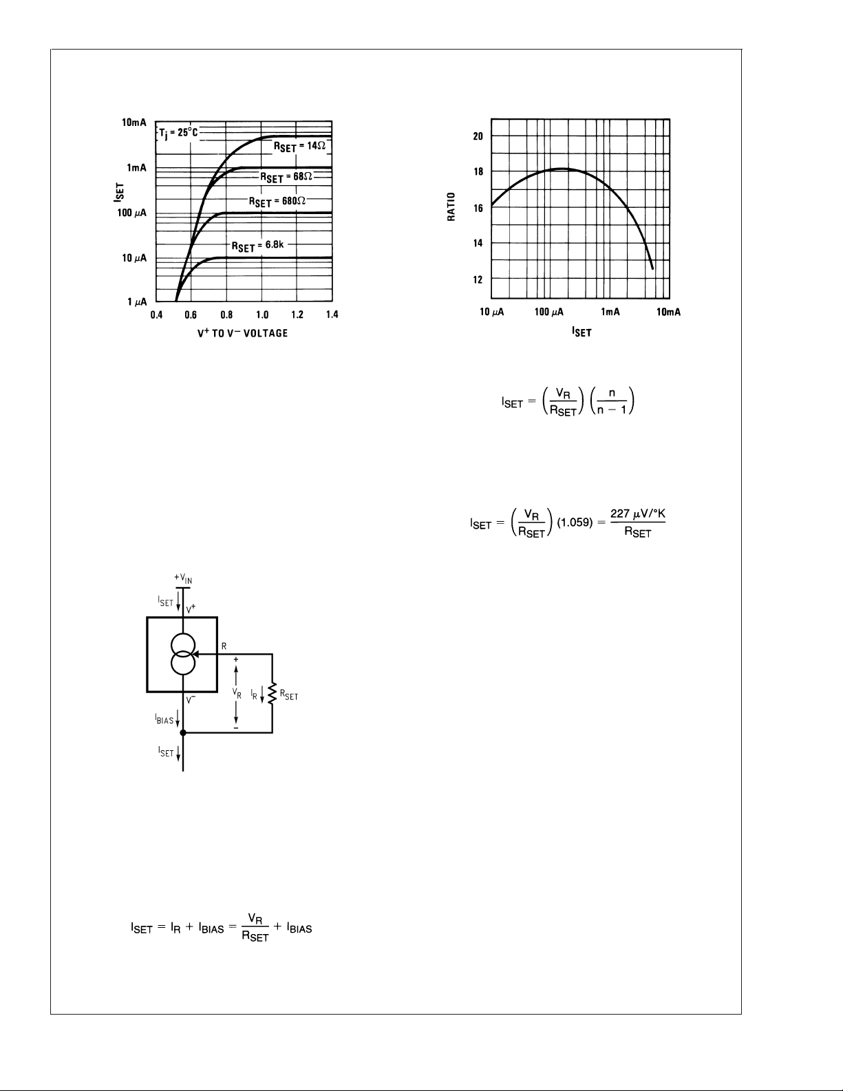
Application Hints
The LM134 has been designed for ease of application, but a
general discussion of design features is presented here to
familiarize the designer with device characteristics which
may not be immediately obvious. These include the effects
of slewing, power dissipation, capacitance, noise, and contact resistance.
CALCULATING R
The total current through the LM134 (I
current going through the SET resistor (I
bias current (I
SET
), as shown in Figure 1.
BIAS
) is the sum of the
SET
) and the LM134’s
R
to I
SET
BIAS
00569703
where n is the ratio of I
SET
to I
as specified in the
BIAS
Electrical Characteristics Section and shown in the graph.
Since n is typically 18 for 2µA ≤ I
≤ 1mA, the equation can
SET
be further simplified to
for most set currents.
00569727
FIGURE 1. Basic Current Source
A graph showing the ratio of these two currents is supplied
under Ratio of I
SET
to I
Characteristics section. The current flowing through R
determined by V
, which is approximately 214µV/˚K (64
R
in the Typical Performance
BIAS
SET
mV/298˚K ∼ 214µV/˚K).
Since (for a given set current) I
, the equation can be rewritten
I
SET
is simply a percentage of
BIAS
SLEW RATE
At slew rates above a given threshold (see curve), the
LM134 may exhibit non-linear current shifts. The slewing
rate at which this occurs is directly proportional to I
= 10µA, maximum dV/dt is 0.01V/µs; at I
I
SET
SET
.At
SET
= 1mA, the
limit is 1V/µs. Slew rates above the limit do not harm the
LM134, or cause large currents to flow.
THERMAL EFFECTS
Internal heating can have a significant effect on current
regulation for I
1V increase across the LM134 at I
greater than 100µA. For example, each
SET
= 1 mA will increase
SET
junction temperature by ≈0.4˚C in still air. Output current
) has a temperature coefficient of ≈0.33%/˚C, so the
(I
SET
change in current due to temperature rise will be (0.4)
(0.33) = 0.132%. This is a 10:1 degradation in regulation
compared to true electrical effects. Thermal effects, therefore, must be taken into account when DC regulation is
critical and I
is
package or the TO-92 leads can reduce this effect by more
exceeds 100µA. Heat sinking of the TO-46
SET
than 3:1.
SHUNT CAPACITANCE
In certain applications, the 15 pF shunt capacitance of the
LM134 may have to be reduced, either because of loading
problems or because it limits the AC output impedance of the
current source. This can be easily accomplished by buffering
the LM134 with an FET as shown in the applications. This
can reduce capacitance to less than 3 pF and improve
www.national.com5
Page 6
Application Hints (Continued)
regulation by at least an order of magnitude. DC characteristics (with the exception of minimum input voltage), are not
affected.
NOISE
Current noise generated by the LM134 is approximately 4
times the shot noise of a transistor. If the LM134 is used as
LM134/LM234/LM334
an active load for a transistor amplifier, input referred noise
will be increased by about 12dB. In many cases, this is
acceptable and a single stage amplifier can be built with a
voltage gain exceeding 2000.
LEAD RESISTANCE
The sense voltage which determines operating current of the
LM134 is less than 100mV. At this level, thermocouple or
lead resistance effects should be minimized by locating the
current setting resistor physically close to the device. Sockets should be avoided if possible. It takes only 0.7Ω contact
resistance to reduce output current by 1% at the 1 mA level.
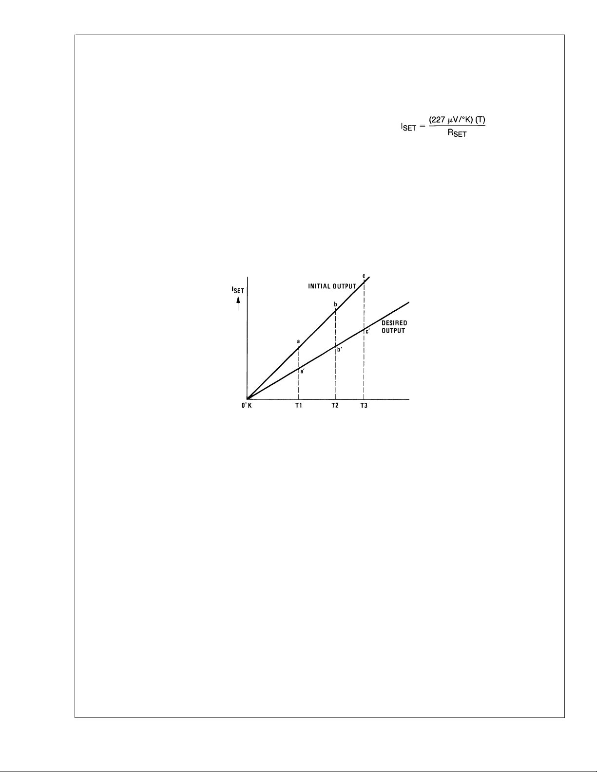
SENSING TEMPERATURE
The LM134 makes an ideal remote temperature sensor because its current mode operation does not lose accuracy
over long wire runs. Output current is directly proportional to
absolute temperature in degrees Kelvin, according to the
following formula:
Calibration of the LM134 is greatly simplified because of the
fact that most of the initial inaccuracy is due to a gain term
(slope error) and not an offset. This means that a calibration
consisting of a gain adjustment only will trim both slope and
zero at the same time. In addition, gain adjustment is a one
point trim because the output of the LM134 extrapolates to
zero at 0˚K, independent of R
or any initial inaccuracy.
SET
FIGURE 2. Gain Adjustment
This property of the LM134 is illustrated in the accompanying
graph. Line abc is the sensor current before trimming. Line
a'b'c' is the desired output. A gain trim done at T2 will move
the output from b to b' and will simultaneously correct the
slope so that the output at T1 and T3 will be correct. This
gain trim can be done on R
or on the load resistor used
SET
to terminate the LM134. Slope error after trim will normally
±
be less than
temperature coefficient resistor must be used for R
A 33 ppm/˚C drift of R
1%. To maintain this accuracy, however, a low
.
SET
will give a 1% slope error because
SET
the resistor will normally see about the same temperature
variations as the LM134. Separating R
from the LM134
SET
requires 3 wires and has lead resistance problems, so is not
00569704
normally recommended. Metal film resistors with less than
20 ppm/˚C drift are readily available. Wire wound resistors
may also be used where best stability is required.
APPLICATION AS A ZERO TEMPERATURE COEFFICENT CURRENT SOURCE
Adding a diode and a resistor to the standard LM134 configuration can cancel the temperature-dependent characteristic of the LM134. The circuit shown in Figure 3 balances
the positive tempco of the LM134 (about +0.23 mV/˚C) with
the negative tempco of a forward-biased silicon diode (about
−2.5 mV/˚C).
www.national.com 6
Page 7
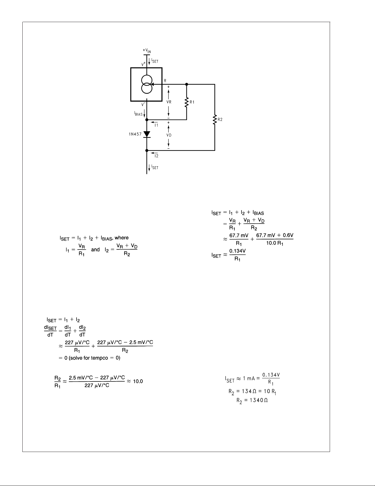
Application Hints (Continued)
LM134/LM234/LM334
00569728
FIGURE 3. Zero Tempco Current Source
The set current (I
uting approximately 50% of the set current, and I
usually included in the I
used for calculations by 5.9%. (See CALCULATING R
) is the sum of I1and I2, each contrib-
SET
term by increasing the VRvalue
1
BIAS.IBIAS
SET
The first step is to minimize the tempco of the circuit, using
the following equations. An example is given using a value of
+227µV/˚C as the tempco of the LM134 (which includes the
component), and −2.5 mV/˚C as the tempco of the
I
BIAS
diode (for best results, this value should be directly measured or obtained from the manufacturer of the diode).
is
.)
This circuit will eliminate most of the LM134’s temperature
coefficient, and it does a good job even if the estimates of the
diode’s characteristics are not accurate (as the following
example will show). For lowest tempco with a specific diode
at the desired I
tested over temperature. If the measured tempco of I
positive, R
negative, R
, however, the circuit should be built and
SET
should be reduced. If the resulting tempco is
2
should be increased. The recommended diode
2
SET
is
for use in this circuit is the 1N457 because its tempco is
centered at 11 times the tempco of the LM134, allowing R
. You can also use this circuit to create a current source
10 R
1
=
2
with non-zero tempcos by setting the tempco component of
the tempco equation to the desired value instead of 0.
EXAMPLE: A 1mA, Zero-Tempco Current Source
First, solve for R
and R2:
1
With the R1to R2ratio determined, values for R1and R
should be determined to give the desired set current. The
formula for calculating the set current at T = 25˚C is shown
below, followed by an example that assumes the forward
voltage drop across the diode (V
across R
and R
is 67.7mV (64 mV + 5.9% to account for I
1
= 10 (from the previous calculations).
2/R1
) is 0.6V, the voltage
D
BIAS
2
The values of R1and R2can be changed to standard 1%
resistor values (R
),
a 0.75% error.
= 133Ω and R2= 1.33kΩ) with less than
1
www.national.com7
Page 8

Application Hints (Continued)
If the forward voltage drop of the diode was 0.65V instead of
the estimate of 0.6V (an error of 8%), the actual set current
will be
LM134/LM234/LM334
an error of less than 5%.
If the estimate for the tempco of the diode’s forward voltage
drop was off, the tempco cancellation is still reasonably
effective. Assume the tempco of the diode is 2.6mV/˚C instead of 2.5mV/˚C (an error of 4%). The tempco of the circuit
is now:
Terminating Remote Sensor for Voltage Output
00569714
Low Output Impedance Thermometer
A 1mA LM134 current source with no temperature compensation would have a set resistor of 68Ω and a resulting
tempco of
So even if the diode’s tempco varies as much as±4% from
its estimated value, the circuit still eliminates 98% of the
LM134’s inherent tempco.
Typical Applications
Ground Referred Fahrenheit Thermometer
*Output impedance of the LM134 at the “R” pin is approximately
where R2is the equivalent external resistance connected from the V−pin
to ground. This negative resistance can be reduced by a factor of 5 or
more by inserting an equivalent resistor R
output.
=(R2/16) in series with the
3
00569706
Low Output Impedance Thermometer
*Select R3 = V
Trim R3 to calibrate
www.national.com 8
/583µA. V
REF
may be any stable positive voltage ≥ 2V
REF
00569715
00569716
Page 9
Typical Applications (Continued)
LM134/LM234/LM334
Higher Output Current
*Select R1 and C1 for optimum stability
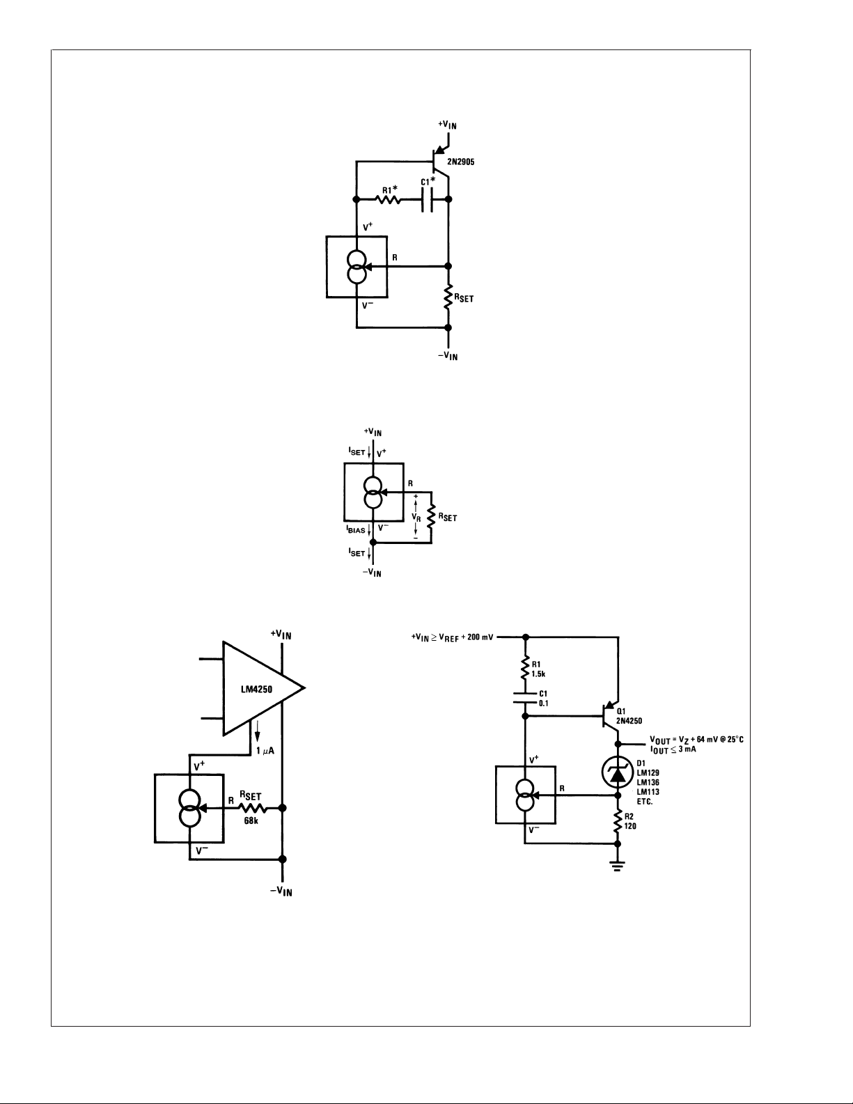
Micropower Bias Low Input Voltage Reference Driver
00569705
Basic 2-Terminal Current Source
00569701
00569717
00569718
www.national.com9
Page 10

Typical Applications (Continued)
LM134/LM234/LM334
Ramp Generator
00569719
1.2V Reference Operates on 10 µA and 2V
*Select ratio of R1 to R2 to obtain zero temperature drift
1.2V Regulator with 1.8V Minimum Input
00569720
Zener Biasing
00569749
Alternate Trimming Technique
*Select ratio of R1 to R2 for zero temperature drift
00569707
www.national.com 10
*For±10% adjustment, select R
00569750
10% high, and make R1 ≈ 3R
SET
SET
Page 11

Typical Applications (Continued)
Buffer for Photoconductive Cell
FET Cascoding for Low Capacitance and/or Ultra High Output Impedance
LM134/LM234/LM334
00569751
*Select Q1 or Q2 to ensure at least 1V across the LM134. Vp(1 −
I
) ≥ 1.2V.
SET/IDSS
00569721
Generating Negative Output Impedance
*Z
≈ −16•R1 (R1/VINmust not exceed I
OUT
00569723
)
SET
00569722
FIGURE 4.
In-Line Current Limiter
00569709
*Use minimum value required to ensure stability of protected device. This
minimizes inrush current to a direct short.
Schematic Diagram
www.national.com11
Page 12

Schematic Diagram (Continued)
LM134/LM234/LM334
00569711
www.national.com 12
Page 13

Physical Dimensions inches (millimeters)
unless otherwise noted
LM134/LM234/LM334
Order Number LM134H, LM234H or LM334H
NS Package Number H03H
www.national.com13
Page 14

Physical Dimensions inches (millimeters) unless otherwise noted (Continued)
LM134/LM234/LM334
SO Package (M)
Order Number LM334M, LM334MX,
LM334SM or LM334SMX
NS Package Number M08A
Order Number LM334Z, LM234Z-3 or LM234Z-6
NS Package Number Z03A
www.national.com 14
Page 15

Notes
LM134/LM234/LM334 3-Terminal Adjustable Current Sources
National does not assume any responsibility for use of any circuitry described, no circuit patent licenses are implied and National reserves
the right at any time without notice to change said circuitry and specifications.
For the most current product information visit us at www.national.com.
LIFE SUPPORT POLICY
NATIONAL’S PRODUCTS ARE NOT AUTHORIZED FOR USE AS CRITICAL COMPONENTS IN LIFE SUPPORT DEVICES OR SYSTEMS
WITHOUT THE EXPRESS WRITTEN APPROVAL OF THE PRESIDENT AND GENERAL COUNSEL OF NATIONAL SEMICONDUCTOR
CORPORATION. As used herein:
1. Life support devices or systems are devices or systems
which, (a) are intended for surgical implant into the body, or
(b) support or sustain life, and whose failure to perform when
properly used in accordance with instructions for use
2. A critical component is any component of a life support
device or system whose failure to perform can be reasonably
expected to cause the failure of the life support device or
system, or to affect its safety or effectiveness.
provided in the labeling, can be reasonably expected to result
in a significant injury to the user.
BANNED SUBSTANCE COMPLIANCE
National Semiconductor certifies that the products and packing materials meet the provisions of the Customer Products Stewardship
Specification (CSP-9-111C2) and the Banned Substances and Materials of Interest Specification (CSP-9-111S2) and contain no ‘‘Banned
Substances’’ as defined in CSP-9-111S2.
National Semiconductor
Americas Customer
Support Center
Email: new.feedback@nsc.com
Tel: 1-800-272-9959
www.national.com
National Semiconductor
Europe Customer Support Center
Fax: +49 (0) 180-530 85 86
Email: europe.support@nsc.com
Deutsch Tel: +49 (0) 69 9508 6208
English Tel: +44 (0) 870 24 0 2171
Français Tel: +33 (0) 1 41 91 8790
National Semiconductor
Asia Pacific Customer
Support Center
Email: ap.support@nsc.com
National Semiconductor
Japan Customer Support Center
Fax: 81-3-5639-7507
Email: jpn.feedback@nsc.com
Tel: 81-3-5639-7560
 Loading...