

Page 1

LM32
Dual Thermal Diode Temperature Sensor with
LM32 Dual Thermal Diode Temperature Sensor with SensorPath
May 2004
SensorPath
™
Bus
General Description
The LM32 is a digital temperature sensor that measures 3
temperature zones and has a single-wire interface compatible with National Semiconductor’s SensorPath bus. SensorPath data is pulse width encoded, thereby allowing the LM32
to be easily connected to many general purpose microcontrollers. Several National Semiconductor Super I/O products include a fully integrated SensorPath master, that when
connected to an LM32 can realize a hardware monitor function that includes limit checking for measured values, autonomous fan speed control and many other functions.
The LM32 measures the temperature of its own die as well
as two external devices such as a processor thermal diode
or a diode connected transistor. The LM32 can resolve temperatures up to 255˚C and down to -256˚C. The operating
temperature range of the LM32 is 0˚C to +125˚C. The address programming pin allows two LM32s to be placed on
one SensorPath bus.
Features
n SensorPath Interface
— 2 hardware programmable addresses
Typical Application
n 2 remote diode temperature sensor zones
n Internal local temperature zone
n 0.5 ˚C resolution
n Measures temperatures up to 140 ˚C
n 14-lead TSSOP package
Key Specifications
n Temperature Sensor Accuracy
n Temperature Range:
— LM32 junction 0 ˚C to +85 ˚C
— Remote Temp Accuracy 0 ˚C to +100 ˚C
n Power Supply Voltage +3.0 V to +3.6 V
n Average Power Supply Current 0.5 mA (typ)
n Conversion Time (all Channels) 22.5ms to 1456ms
±
3 ˚C (max)
Applications
n Microprocessor based equipment
(Motherboards, Video Cards, Base-stations, Routers,
ATMs, Point of Sale, …)
n Power Supplies
20071101
SensorPath™is a trademark of National Semiconductor Corporation
© 2004 National Semiconductor Corporation DS200711 www.national.com
™
Bus
Page 2

Connection Diagram
LM32
TSSOP-14
Order
Number
LM32CIMT LM32
LM32CIMTX LM32
Package
Marking
CIMT
CIMT
NS
Package
Number
MTC14C 94 units per
MTC14C 2500 units in
Transport
Media
rail
tape and reel
Top View
National Package Number MTC14C
20071102
Pin Description
Pin Number Pin Name Description Typical Connection
1, 6, 7,12, 13,
14
2 GND Ground System ground
3 V+/+3.3V_SBY Positive power supply pin Connected system 3.3 V standby power and
4 SWD SensorPath Bus line; Open-drain
5 ADD Digital input - device number select
8, 10 D1-, D2- Thermal diode analog voltage
9, 11 D1+, D2+ Thermal diode analog current
NC No Connect May be tied to V+, GND or left floating
to a 0.1 µF bypass capacitor in parallel with
100 pF. A bulk capacitance of approximately
10 µF needs to be in the near vicinity of the
LM32.
Super I/O, Pull-up resistor, 1.6k
output
Pull-up to 3.3 V or pull-down to GND resistor,
input for the serial bus device
number
output and negative monitoring
input
output and positive monitoring input
10k; must never be left floating
Remote Thermal Diode cathode
(THERM_DC) - Diode 1 should always be
connected to the processor thermal diode.
Diode 2 may be connected to an MMBT3904
or GPU thermal diode. A 100 pF capacitor
should be connected between respective D-
and D+ for noise filtering.
Remote Thermal Diode anode (THERM_DA) -
Diode 1 should always be connected to the
processor thermal diode. Diode 2 may be
connected to an MMBT3904 or GPU thermal
diode. A 100 pF capacitor should be
connected between respective D- and D+ for
noise filtering.
www.national.com 2
Page 3
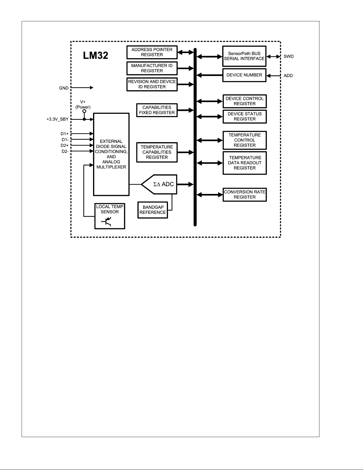
Block Diagram
LM32
20071103
www.national.com3
Page 4

Absolute Maximum Ratings
LM32
(Notes 2, 1)
Supply Voltage (V
+
) −0.5 V to 6.0 V
Storage Temperature −65˚C to +150˚C
Soldering process must comply with National’s reflow
temperature profile specifications. Refer to
www.national.com/packaging/. (Note 6)
Voltage at Any Digital Input or
Output Pin −0.5 V to 6.0 V
Voltage on D1+ and D2+ −0.5 V to (V+ + 0.05 V)
Current on D1- and D2-
Input Current per Pin(Note 3)
Package Input Current (Note 3)
±
1mA
±
5mA
±
30 mA
Package Power Dissipation (Note 4)
Output Sink Current 10 mA
ESD Susceptibility (Note 5)
Human Body Model 2500 V
Operating Ratings
(Notes 1, 2)
Temperature Range for Electrical Characteristics
LM32CIMT (T
MIN≤TA≤TMAX
Operating Temperature Range 0˚C ≤ T
Remote Diode Temperature (T
Range -5˚C ≤T
Supply Voltage Range (V+) +3.0 V to +3.6 V
) 0˚C ≤ TA≤ +85˚C
)
D
Machine Model 250 V
DC Electrical Characteristics
The following specifications apply for V+ = +3.0 VDCto +3.6 VDC, and all analog source impedance RS=50Ω unless other-
wise specified in the conditions. Boldface limits apply for LM32CIMT T
= +25˚C. TAis the ambient temperature of the LM32; TJis the junction temperature of the LM32; TDis the junction tem-
T
A
A=TJ=TMIN
=0˚C to T
perature of the remote thermal diode.
POWER SUPPLY CHARACTERISTICS
Symbol Parameter Conditions
Typical
(Note 7)
V+ Power Supply Voltage 3.3
I+
Shutdown
Shutdown Power Supply Current
SensorPath Bus Inactive
(Note 9)
SensorPath Bus Inactive; all
I+
Average
I+
Peak
Average Power Supply Current
Peak Power Supply Current
sensors enabled;
=182 ms; (Note 9)
t
CONV
SensorPath Bus Inactive
(Note 9)
Power-On Reset Threshold Voltage
TEMPERATURE-TO-DIGITAL CONVERTER CHARACTERISTICS
Parameter Conditions
Temperature Accuracy Using the Remote Thermal
Diode, see (Note 11) for Thermal Diode Processor
Type.
Temperature Accuracy Using the Local Diode T
T
J
= 0˚C to
TD= +25˚C
+85˚C
T
= 0˚C to
J
+85˚C
T
= 0˚C to
J
+85˚C
= 0˚C to +85˚C (Note 10)
J
TD= 0˚C to
+100˚C
TD= +100˚C to
+125˚C
Typical
(Note 7)
Remote Diode and Local Temperature Resolution 10 Bits
D− Source Voltage 0.7 V
Diode Source Current
(V
D+−VD−
Low Current 11.75 µA
) = +0.65 V; High Current 188 280 µA (max)
Diode Source Current High Current to Low Current
Ratio
=85˚C; all other limits
MAX
Limits
(Note 8)
3.0
3.6
260 420 µA (max)
900 µA (max)
3.3 mA (max)
1.6 V (min)
2.8 V (max)
Limits
(Note 8)
±
1
±
1
±
2.5 ˚C (max)
±
3 ˚C (max)
±
4 ˚C (max)
±
3 ˚C (max)
0.5 ˚C
16
≤ +125˚C
A
≤+140 ˚C
D
Units
(Limit)
V (min)
V (max)
Units
(Limits)
www.national.com 4
Page 5

SWD and ADD DIGITAL INPUT CHARACTERISTICS
Symbol Parameter Conditions
SWD Logical High Input Voltage 2.1 V (min)
SWD Logical Low Input Voltage 0.8 V (max)
ADD Logical High Input Voltage 90%xV+ V (min)
ADD Logical Low Input Voltage 10%xV+ V (max)
Input Hysteresis 300 mV
SWD and ADD Input Current GND ≤ VIN≤ V+
SWD Input Current with V+ Open or
Grounded
GND ≤ V
≤ 3.6V,
IN
and V+ Open or
V
V
IH
V
IL
V
IH
V
IL
HYST
I
L
GND
C
IN
Digital Input Capacitance 10 pF
SWD DIGITAL OUTPUT CHARACTERISTICS
Symbol Parameter Conditions
V
OL
Open-drain Output Logic “Low”
Voltage
I
OH
C
OUT
Open-drain Output Off Current
Digital Output Capacitance 10 pF
IOL= 4mA 0.4 V (max)
I
= 50µA 0.2 V (max)
OL
Typical
(Note 7)
Limits
(Note 8)
V+ + 0.5 V (max)
-0.5 V (min)
±
0.005
±
0.005 µA
Typical
(Note 7)
±
0.005
±
10 µA (max)
Limits
(Note 8)
±
10 µA (max)
LM32
Units
(Limit)
Units
(Limit)
AC Electrical Characteristics
The following specification apply for V+ = +3.0 VDCto +3.6 VDC, unless otherwise specified. Boldface limits apply for
T
A=TJ=TMIN
=0˚C to T
specification revision 0.98. Please refer to that speciation for further details.
Symbol Parameter Conditions
HARDWARE MONITOR CHARACTERISTICS
t
CONV
Total Monitoring Cycle Time (Note 12) All Temperature readings
SensorPath Bus CHARACTERISTICS
t
INACT
t
f
t
r
SWD fall time (Note 15) R
SWD rise time (Note 15) R
Minimum inactive time (bus at high level)
guaranteed by the slave before an attention
request
t
Mtr0
Master drive for Data Bit 0 write and for Data
Bit 0-1read
t
Mtr1
t
SFEdet
t
SLout1
t
MtrS
t
SLoutA
t
RST
Master drive for Data Bit 1 write 35.4 µs (min)
Time allowed for LM32 activity detection 9.6 µs (max)
LM32 drive for Data Bit 1 read by master 28.3 µs (min)
Master drive for Start Bit 80 µs (min)
LM32 drive for Attention Request 165 µs (min)
Master or LM32 drive for Reset 354 µs (min)
=85˚C; all other limits TA=TJ= 25˚C. The SensorPath Characteristics conform to the SensorPath
MAX
Typical
(Note 7)
Limits
(Note 8)
182 163.8 ms (min)
(Default)
=1.25 kΩ±30%,
pull-up
=400 pF
C
L
=1.25 kΩ±30%,
pull-up
=400 pF
C
L
200.2 ms (max)
300 ns (max)
1000 ns (max)
11 µs (min)
11.8 µs (min)
17.0 µs (max)
48.9 µs (max)
38.3 µs (max)
109 µs (max)
228 µs (max)
Units
(Limits)
www.national.com5
Page 6
AC Electrical Characteristics (Continued)
LM32
The following specification apply for V+ = +3.0 VDCto +3.6 VDC, unless otherwise specified. Boldface limits apply for
T
A=TJ=TMIN
=0˚C to T
=85˚C; all other limits TA=TJ= 25˚C. The SensorPath Characteristics conform to the SensorPath
MAX
specification revision 0.98. Please refer to that speciation for further details.
Symbol Parameter Conditions
t
RST_MAX
Maximum drive of SWD by an LM32, after the
Typical
(Note 7)
Limits
(Note 8)
500 ms (max)
power supply is raised above 3V
Note 1: Absolute Maximum Ratings indicate limits beyond which damage to the device may occur. Operating Ratings indicate conditions for which the device is
functional, but do not guarantee performance limits. For guaranteed specifications and test conditions, see the Electrical Characteristics. The guaranteed
specifications apply only for the test conditions listed. Some performance characteristics may degrade when the device is not operated under the listed test
conditions.
Note 2: All voltages are measured with respect to GND, unless otherwise noted.
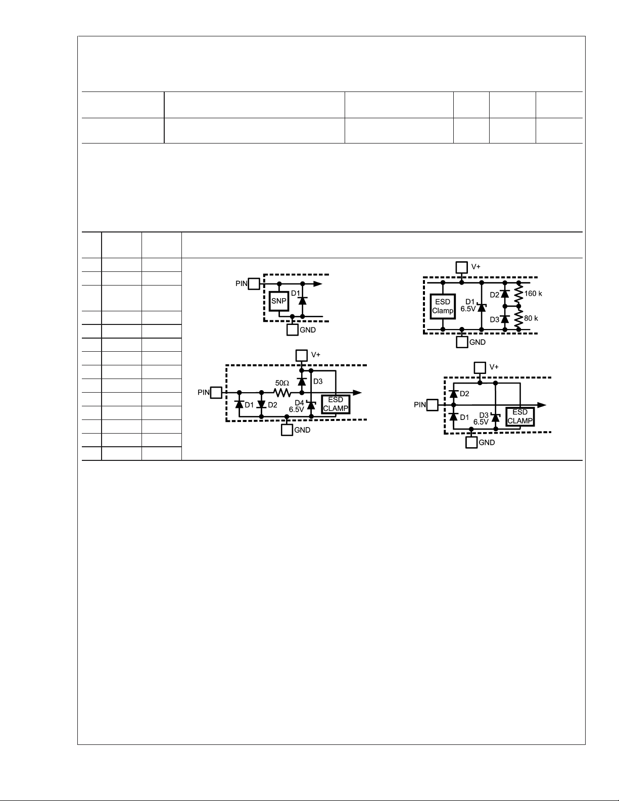
Note 3: When the input voltage (V
components and/or ESD protection circuitry are shown below for the LM32’s pins. The nominal breakdown voltage of the zener is 6.5 V. SNP stands for snap-back
device.
) at any pin exceeds the power supplies (V
IN
IN
<
GND or V
>
V+), the current at that pin should be limited to 5 mA. Parasitic
IN
Units
(Limits)
PIN#Pin
Name
Pin
Circuit
All Input Structure Circuits
1NC A
2 GND B
V+/
3
3.3V SB
B
4 SWD A
5 ADD A
6 NC none
7 NC none
Circuit A
Circuit B
8 D1- C
9 D1+ D
10 D2- C
11 D2+ D
12 NC none
13 NC none
14 NC A
Note 4: Thermal resistance junction-to-ambient in still air when attached to a printed circuit board with 1 oz. foil is 148 ˚C/W.
Note 5: Human body model, 100 pF discharged through a 1.5 kΩ resistor. Machine model, 200 pF discharged directly into each pin.
Note 6: Reflow temperature profiles are different for lead-free and non lead-free packages.
Note 7: “Typicals” are at T
Note 8: Limits are guaranteed to National’s AOQL (Average Outgoing Quality Level).
Note 9: The supply current will not increase substantially with a SensorPath transaction.
Note 10: Local temperature accuracy does not include the effects of self-heating. The rise in temperature due to self-heating is the product of the internal power
dissipation of the LM32 and the thermal resistance. See (Note 4) for the thermal resistance to be used in the self-heating calculation.
Note 11: The accuracy of the LM32CIMT is guaranteed when using the thermal diode of an Intel 90 nm Pentium 4 processor or any thermal diode with a non-ideality
factor of 1.011 and series resistance of 3.33Ω. When using a MMBT3904 type transistor as a thermal diode the error band will be typically shifted by -4.5 ˚C.
Note 12: This specification is provided only to indicate how often temperature data are updated.
Note 13: The output fall time is measured from (V
Note 14: The output rise time is measured from (V
Note 15: The rise and fall times are not tested but guaranteed by design.
= 25˚C and represent most likely parametric norm. They are to be used as general reference values not for critical design calculations.
A
IH min
IL max
Circuit C
)to(V
IL max
)to(V
IH min
Circuit D
).
).
www.national.com 6
Page 7

Timing Diagrams
LM32
20071104
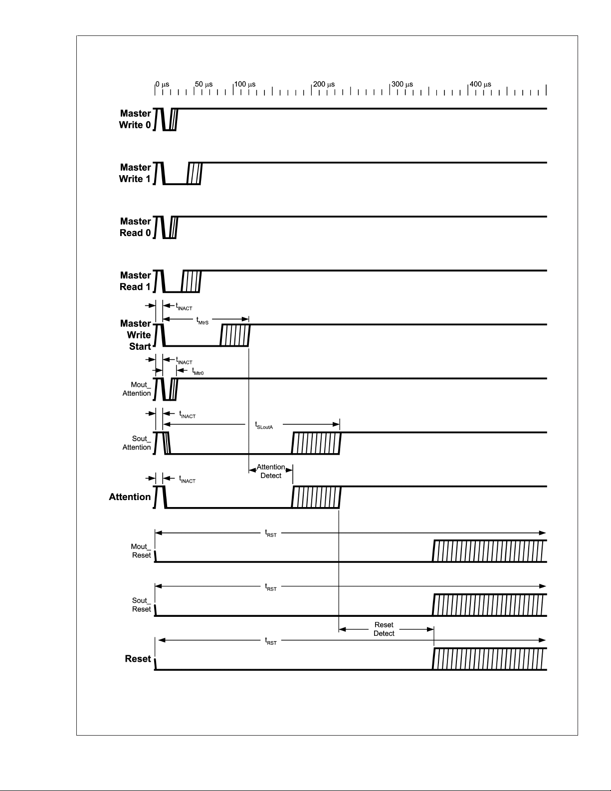
FIGURE 1. Timing for Data Bits 0, 1 and Start Bit. See Section 1.2 "SensorPath BIT SIGNALING" for further details.
www.national.com7
Page 8
Timing Diagrams (Continued)
LM32
FIGURE 2. Timing for Attention Request and Reset. See Section 1.2 "SensorPath BIT SIGNALING" for further details.
www.national.com 8
20071105
Page 9
Typical Performance Characteristics
LM32
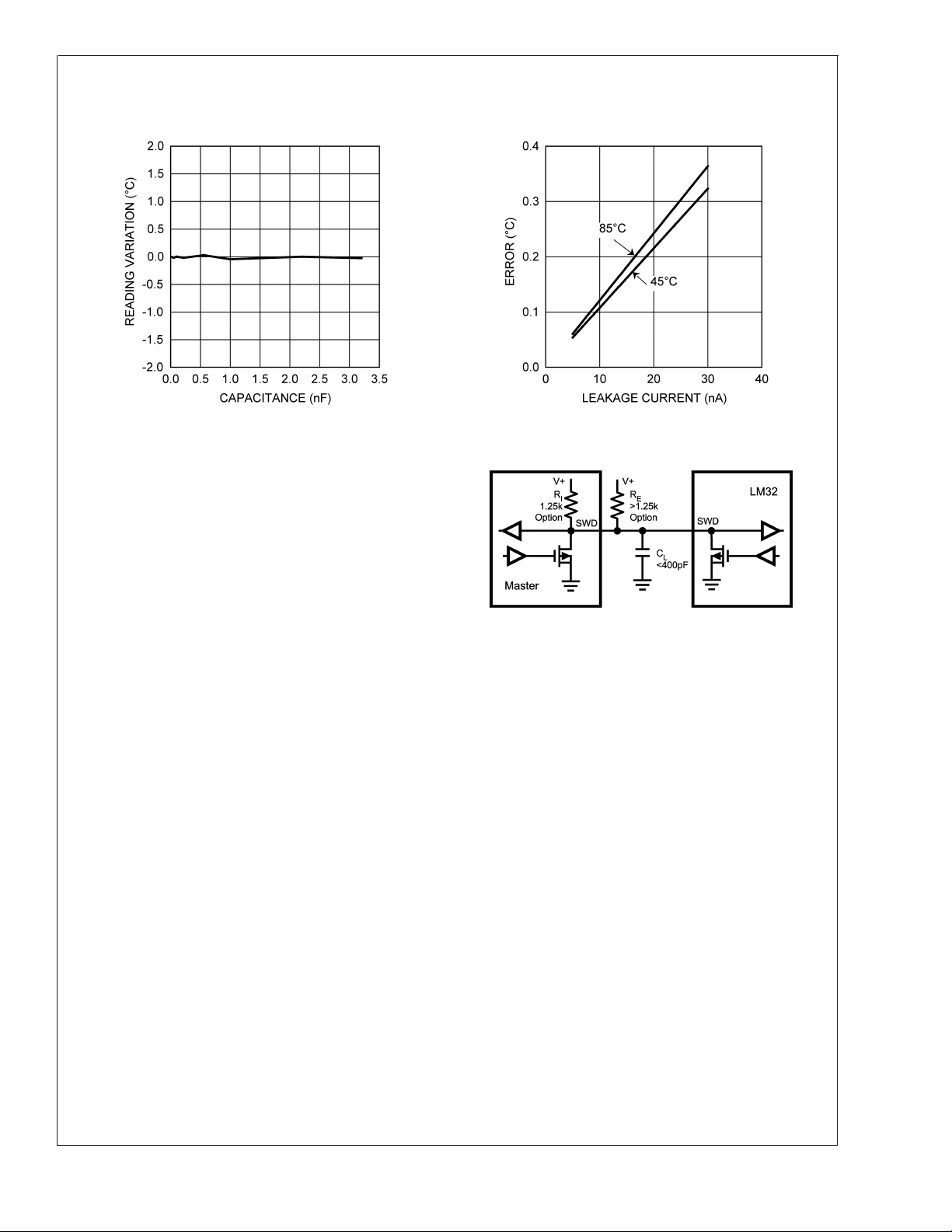
Remote Diode Temperature Reading Sensitivity to Diode
Filter Capacitance
20071121 20071122
1.0 Functional Description
The LM32 measures 3 temperature zones. The LM32 uses a
temperature sensing method. A differential voltage,
∆V
be
representing temperature, is digitized using a Sigma-Delta
analog to digital converter. The digitized data can be retrieved over a simple single-wire interface called SensorPath. SensorPath has been defined by National Semiconductor and is optimized for hardware monitoring. National
offers a royalty-free license in connection with its intellectual
property rights in the SensorPath bus.
The LM32 has one address pin to allow up to two LM32s to
be connected to one SensorPath bus. The physical interface
of SensorPath’s SWD signal is identical to the familiar industry standard SMBus SMBDAT signal. The digital information
is encoded in the pulse width of the signal being transmitted.
Every bit can be synchronized by the master simplifying the
implementation of the master when using a micro-controller.
For micro-controller’s with greater functionality an asynchronous attention signal can be transmitted by the LM32 to
interrupt the micro-controller and notify it that temperature
data has been updated in the readout registers.
To optimize the LM32’s power consumption to the system
requirements, the LM32 has a shutdown mode and supports
multiple conversion rates.
1.1 SensorPath BUS SWD
SWD is the Single Wire Data line used for communication.
SensorPath uses 3.3V single-ended signaling, with a pull-up
resistor and open-drain low-side drive (see Figure 3). For
timing purposes SensorPath is designed for capacitive loads
) of up to 400pF. Note that in many cases a 3.3V standby
(C
L
rail of the PC will be used as a power supply for both the
sensor and the master. Logic high and low voltage levels for
SWD are TTL compatible. The master may provide an internal pull-up resistor. In this case the external resistor is not
needed. The minimum value of the pull-up resistor must take
into account the maximum allowable output load current of
4mA.
Thermal Diode Capacitor or PCB Leakage Current Effect
on Remote Diode Temperature Reading
20071107
FIGURE 3. SensorPath SWD simplified schematic
1.2 SensorPath BIT SIGNALING
Signals are transmitted over SensorPath using pulse-width
encoding. There are five types of "bit signals":
Data Bit 0
•
Data Bit 1
•
Start Bit
•
Attention Request
•
Reset
•
All the "bit signals" involve driving the bus to a low level. The
duration of the low level differentiates between the different
"bit-signals". Each "bit signal" has a fixed pulse width. SensorPath supports a Bus Reset Operation and Clock Training
sequence that allows the slave device to synchronize its
internal clock rate to the master. Since the LM32 meets the
±
15% timing requirements of SensorPath, the LM32 does
not require the Clock Training sequence and does not support this feature. This section defines the "bit signal" behavior in all the modes. Please refer to the timing diagrams in
the Electrical Characteristics section (Figure 1 and Figure 2)
while going through this section. Note that the timing diagrams for the different types of "bit signals" are shown
together to better highlight the timing relationships between
them. However, the different types of "bit signals" appear on
SWD at different points in time. These timing diagrams show
the signals as driven by the master and the LM32 slave as
well as the signal as seen when probing SWD. Signal labels
that begin with the label Mout_ depict a drive by the master.
www.national.com9
Page 10

1.0 Functional Description (Continued)
LM32
Signal labels that begin with the label Slv_ depict the drive by
the LM32. All other signals show what would be seen when
probing SWD for a particular function (e.g. "Master Wr 0" is
the Master transmitting a Data Bit with the value of 0).
1.2.1 Bus Inactive
The bus is inactive when the SWD signal is high for a period
of at least t
. The bus is inactive between each "bit
INACT
signal".
1.2.2 Data Bit 0 and 1
All Data Bit signal transfers are started by the master. A Data
Bit 0 is indicated by a "short" pulse; a Data Bit 1 is indicated
by a longer pulse. The direction of the bit is relative to the
master, as follows:
Data Write - a Data Bit transferred from the master to the
•
LM32.
Data Read - a Data Bit transferred from the LM32 to the
•
master.
A master must monitor the bus as inactive before starting a
Data Bit (Read or Write).
A master initiates a data write by driving the bus active (low
level) for the period that matches the data value (t
for a write of "0" or "1", respectively). The LM32 will detect
that the SWD becomes active within a period of t
will start measuring the duration that the SWD is active in
order to detect the data value.
A master initiates a data read by driving the bus for a period
. The LM32 will detect that the SWD becomes active
of t
Mtr0
within a period of t
. For a data read of "0", the LM32
SFEdet
will not drive the SWD. For a data read of "1" the LM32 will
start within t
. Both master and LM32 must monitor the time at
t
SLout1
to drive the SWD low for a period of
SFEdet
which the bus becomes inactive to identify a data read of "0"
or "1".
During each Data Bit, both the master and all the LM32s
must monitor the bus (the master for Attention Request and
Reset; the LM32s for Start Bit, Attention Request and Reset)
by measuring the time SWD is active (low). If a Start Bit,
Attention Requests or Reset "bit signal" is detected, the
current "bit signal" is not treated as a Data Bit.
Note that the bit rate of the protocol varies depending on the
data transferred. Thus, the LM32 has a value of "0" in
reserved or unused register bits for bus bandwidth efficiency.
1.2.3 Start Bit
A master must monitor the bus as inactive before beginning
a Start Bit.
The master uses a Start Bit to indicate the beginning of a
transfer. LM32s will monitor for Start Bits all the time, to allow
synchronization of transactions with the master. If a Start Bit
occurs in the middle of a transaction, the LM32 being addressed will abort the current transaction. In this case the
transaction is not "completed" by the LM32 (see Section 1.3
"SensorPath Bus Transactions").
During each Start Bit, both the master and all the LM32s
must monitor the bus for Attention Request and Reset, by
Mtr0
SFEdet
or t
Mtr1
, and
measuring the time SWD is active (low). If an Attention
Request or Reset condition is detected, the current "bit
signal" is not treated as a Start Bit. The master may attempt
to send the Start Bit at a later time.
1.2.4 Attention Request
The LM32 may initiate an Attention Request when the SensorPath bus is inactive.
Note that a Data Bit, or Start Bit, from the master may start
simultaneously with an Attention Request from the LM32. In
addition, two LM32s may start an Attention Request simultaneously. Due to its length, the Attention Request has priority over any other "bit signal", except Reset. Conflict with
Data Bits and Start Bits are detected by all the devices, to
allow the bits to be ignored and re-issued by their originator.
The LM32 will either check to see that the bus is inactive
before starting an Attention Request, or start the Attention
Request within the t
active. The LM32 will drive the signal low for t
time interval after SWD becomes
SFEdet
SLoutA
time.
After this, both the master and the LM32 must monitor the
bus for a Reset Condition. If a Reset condition is detected,
the current "bit signal" is not treated as an Attention Request.
After Reset, an Attention Request can not be sent before the
master has sent 14 Data Bits on the bus. See Section 1.3.5
for further details on Attention Request generation.
1.2.5 Bus Reset
The LM32 issues a Reset at power up. The master must also
generate a Bus Reset at power-up for at least the minimum
reset time, it must not rely on the LM32. SensorPath puts no
limitation on the maximum reset time of the master. Following a Bus Reset, the LM32 may generate an Attention Request only after the master has sent 14 Data Bits on the bus.
See Section 1.3.5 for further details on Attention Request
generation.
1.3 SensorPath BUS TRANSACTIONS
SensorPath is designed to work with a single master and up
to seven slave devices. Each slave has a unique address.
The LM32 supports up to 2 device addresses that are selected by the state of the address pin ADD. The Register Set
of the LM32 is defined in Section 2.0.
1.3.1 Bus Reset Operation
A Bus Reset Operation is global on the bus and affects only
the communication interface of all the devices connected to
it. The Bus Reset operation does not affect either the contents of the device registers, or device operation, to the
extent defined in LM32 Register Set, see Section 2.0.
The Bus Reset operation is performed by generating a Reset
signal on the bus. The master must apply Reset after powerup, and before it starts operation. The Reset signal end will
be monitored by all the LM32s on the bus.
After the Reset Signal the SensorPath specification requires
that the master send a sequence of 8 Data Bits with a value
of "0", without a preceding Start Bit. This is required to
enable slaves that "train" their clocks to the bit timing. The
LM32 does not require nor does it support clock training.
www.national.com 10
Page 11

1.0 Functional Description (Continued)
FIGURE 4. Bus Reset Transaction
LM32
20071108
1.3.2 Read Transaction
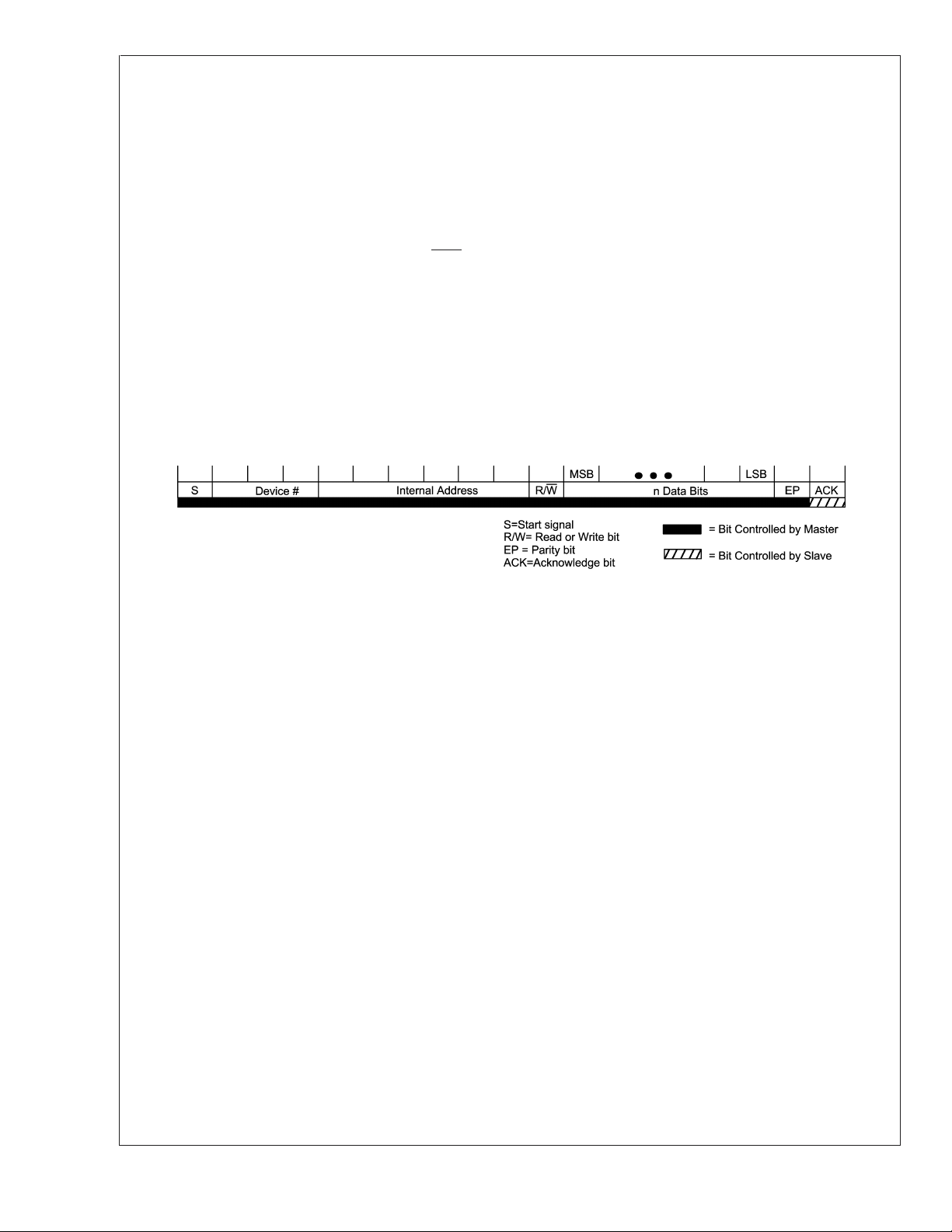
During a read transaction, the master reads data from a
register at a specified address within a slave. A read transaction begins with a Start Bit and ends with an ACK bit, as
shown in Figure 5.
Device Number This is the address of the LM32 device
•
accessed. Address "000" is a broadcast address and can
be responded to by all the slave devices. The LM32
ignores the broadcast address during a read transaction.
Internal Address The address of a register within the
•
LM32 that is read.
Read/Write (R/W) A "1" indicates a read transaction.
•
Data Bits During a read transaction the data bits are
•
driven by the LM32. Data is transferred serially with the
most significant bit first. This allows throughput optimization based on the information that needs to be read.
The LM32 supports 8-bit or 16-bit data fields, as described in Section 2.0 "Register Set".
Even Parity (EP) This bit is based on all preceding bits
•
(device number, internal address, Read/Write and data
bits) and the parity bit itself. The parity -number of 1’s - of
all the preceding bits and the parity bit must be even - i.e.,
the result must be 0. During a read transaction, the EP bit
is sent by the LM32 to the master to allow the master to
check the received data before using it.
Acknowledge (ACK) During a read transaction the ACK
•
bit is sent by the master indicating that the EP bit was
received and was found to be correct, when compared to
the data preceding it, and that no conflict was detected
on the bus (excluding Attention Request - see Section
1.3.5 "Attention Request Transaction"). A read transfer is
considered "complete" only when the ACK bit is received.
A transaction that was not positively acknowledged is not
considered "complete" by the LM32 and following are
performed:
— The BER bit in the LM32 Device Status register is set
— The LM32 generates an Attention Request before, or
together with the Start Bit of the next transaction
A transaction that was not positively acknowledged is
also not considered "complete" by the master (i.e. internal operations related to the transaction are not performed). The transaction may be repeated by the master,
after detecting the source of the Attention Request (the
LM32 that has a set BER bit in the Device Status register). Note that the SensorPath protocol neither forces, nor
automates re-execution of the transaction by the master.
The values of the ACK bit are:
— 1: Data was received correctly
— 0: An error was detected (no-acknowledge).
FIGURE 5. Read Transaction, master reads data from LM32
1.3.3 Write Transaction
In a write transaction, the master writes data to a register at
a specified address in the LM32. A write transaction begins
with a Start Bit and ends with an ACK Data Bit, as show in
Figure 6.
Device Number This is the address of the slave device
•
accessed. Address "000" is a broadcast address and is
responded to by all the slave devices. The LM32 responds to broadcast messages to the Device Control
Register.
20071109
Internal Address This is the register address in the
•
LM32 that will be written.
Read/Write (R/W) A "0" data bit directs a write transac-
•
tion.
www.national.com11
Page 12
1.0 Functional Description (Continued)
LM32
Data Bits This is the data written to the LM32 register,
•
are driven by the master. Data is transferred serially with
the most significant bit first. The number of data bits may
vary from one address to another, based on the size of
the register in the LM32. This allows throughput optimization based on the information that needs to be written.
The LM32 supports 8-bit or 16-bit data fields, as described in Section 2.0 "Register Set".
Even Parity (EP) This data bit is based on all preceding
•
bits (Device Number, Internal Address, Read/Write and
Data bits) and the Even Parity bit itself. The parity (number of 1’s) of all the preceding bits and the parity bit must
be even - i.e. the result must be 0. During a write transaction, the EP bit is sent by the master to the LM32 to
allow the LM32 to check the received data before using it.
Acknowledge (ACK) During the write transaction the
•
ACK bit is sent by the LM32 indicating to the master that
the EP was received and was found correct, and that no
conflict was detected on the bus (excluding Attention
Request - see Section 1.3.5 "Attention Request Transaction"). A write transfer is considered "completed" only
when the ACK bit is generated. A transaction that was not
positively acknowledged is not considered complete by
the LM32 (i.e. internal operation related to the transaction
are not performed) and the following are performed:
— The BER bit in the LM32 Device Status register is set;
— The LM32 generates an Attention Request before, or
together with the Start Bit of the next transaction
A transaction that was not positively acknowledged is
also not considered "complete" by the master (i.e. internal operations related to the transaction are not performed). The transaction may be repeated by the master,
after detecting the source of the Attention Request (the
LM32 that has a set BER bit in the Device Status register). Note that the SensorPath protocol neither forces, nor
automates re-execution of the transaction by the master.
The values of the ACK bit are:
— 1: Data was received correctly;
— 0: An error was detected (no-acknowledge).
FIGURE 6. Write Transaction, master write data to LM32
1.3.4 Read and Write Transaction Exceptions
This section describes master and LM32 handling of special
bus conditions, encountered during either Read or Write
transactions.
If an LM32 receives a Start Bit in the middle of a transaction,
it aborts the current transaction (the LM32 does not "complete" the current transaction) and begins a new transaction.
Although not recommend for SensorPath normal operation,
this situation is legitimate, therefore it is not flagged as an
error by the LM32 and Attention Request is not generated in
response to it. The master generating the Start Bit, is responsible for handling the not "complete" transaction at a
"higher level".
If LM32 receives more than the expected number of data bits
(defined by the size of the accessed register), it ignores the
unnecessary bits. In this case, if both master and LM32
identify correct EP and ACK bits they "complete" the transaction. However, in most cases, the additional data bits differ
from the correct EP and ACK bits. In this case, both the
master and the LM32 do not "complete" the transaction. In
addition, the LM32 performs the following:
the BER bit in the LM32 Device Status register is set
•
the LM32 generates an Attention Request
•
If the LM32 receives less than the expected number of data
bits (defined by the size of the accessed register), it waits
indefinitely for the missing bits to be sent by the master. If
then the master sends the missing bits, together with the
correct EP/ACK bits, both master and LM32 "complete" the
transaction. However, if the master starts a new transaction
20071110
generating a Start Bit, the LM32 aborts the current transaction (the LM32 does not "complete" the current transaction)
and begins the new transaction. The master is not notified by
the LM32 of the incomplete transaction.
1.3.5 Attention Request Transaction
Attention Request is generated by the LM32 when it needs
the attention of the master. The master and all LM32s must
monitor the Attention Request to allow bit re-sending in case
of simultaneous start with a Data Bit or Start Bit transfer.
Refer to the "Attention Request" section, Section 1.2.4 in the
"Bit Signaling" portion of the data sheet.
The LM32 will generate an Attention Request using the
following rules:
1. A Function event that sets the Status Flag has occurred
and Attention Request is enabled and
2. The "physical" condition for an Attention Request is met
(i.e., the bus is inactive), and
3. At the first time 2 is met after 1 occurred, there has not
been an Attention request on the bus since a read of the
Device Status register, or since a Bus Reset.
OR
1. A bus error event occurred, and
2. the "physical" condition for an Attention Request is met
(i.e., the bus is inactive), and
3. At the first time 2. is met after 1 occurred, there has not
been a Bus Reset.
www.national.com 12
Page 13

1.0 Functional Description (Continued)
All devices (master or slave) must monitor the bus for an
Attention Request signal. The following notes clarify the
intended system operation that uses the Attention Request
Indication.
Masters are expected to use the attention request as a
•
trigger to read results from the LM32. This is done in a
sequence that covers all LM32s. This sequence is referred to as "master sensor read sequence".
After an Attention Request is sent by an LM32 until after
•
the next read from the Device Status register the LM32
does not send Attention Requests for a function event
since it is guaranteed that the master will read the Status
register as part of the master sensor read sequence.
Note that the LM32 will send an attention for BER, regardless of the Status register read, to help the master
with any error recovery operations and prevent deadlocks.
A master must record the Attention Request event. It
•
must then scan all slave devices in the system by reading
LM32
their Device Status register and must handle any pending
event in them before it may assume that there are no
more events to handle.
Note: there is no indication of which slave has sent the
request. The requirement that multiple requests are not sent
allows the master to know within one scan of register reads
that there are no more pending events.
1.3.6 Fixed Device Number Setting
The LM32 device number is defined by strapping of the ADD
pin. The LM32 will wake (after Device Reset) with the Device
Number field of the Device Number register set to the address as designated in Section 2.3 "Device Number". It is the
responsibility of the system designer to avoid having two
devices with the same Device Number on the bus.
Devices should be detected by the master by a read operation of the Device Number register. The read returns "000" if
there is no device at that address on the bus (the EP bit must
be ignored).
www.national.com13
Page 14

2.0 Register Set
LM32
2.1 REGISTER SET SUMMARY
Reg
Register
Add
000 000
000 001
000 010
000 011
000 100
000 101
001 000
001 001
001 010
001 011
-011 111
0Bh-1Fh
100 000
100 001
-111 111
21h-3Fh
Name
Device
00h
Number
Manufacturer
01h
ID
Device ID R 23h
02h
Capabilities
03h
Fixed
Device
04h
Status
Device
05h
Control
Temperature
08h
Capabilities
Processor/
Remote
Temperature
Data
Readout
09h
Local
Temperature
Data
Readout
Temperature
0Ah
Control
Reserved R Undefined
Conversion
20h
Rate
Undefined
Registers
P
R/
W
R * Not Available
R 100Bh 0001000000001011
R 01h
R 0h Not Available BER
R/
W
R 0549h
R
R/
W
R/
W
R Undefined
Bit
O
R
Val
0h
0h
2h Not Available
Bit14Bit13Bit12Bit11Bit10Bit9Bit8Bit7Bit6Bit5Bit4Bit3Bit2Bit
15
MSb
Reserved
00000
RevID Device ID
0000000000100011
Reserved
0000000000000001
Reserved
00 000
Reserved
00000000000 0
Int
Reserved # of Remotes
0000010101001001
MSb
128
Sign
000000000000
64˚C 32˚C 16˚C 8˚C 4˚C 2˚C
˚C
Reserved
Sens
Rout
Sign 10-Bits
Size
LSb
1
0.5
˚C
˚C
000000
ERF1
EnF1
Res
00 0
Res Res Res
00 00
Reserved
See Section 2.3
FuncDescriptor 1
(Temperature)
Reserved
Res
Low
Pwr
SNUM
EN2 EN1 EN0 ATE
Resolution
Bit
1
LSb
SF1
Shut
downReset
0.5˚C
Res
EF
CR1 CR0
0
* Depends on state of ADD pins see Section 2.3 "Device Number".
2.2 DEVICE RESET OPERATION
A Device Reset operation is performed in the following conditions:
At device power-up.
•
When the Reset bit in the Device Control register is set to 1 (see Section 2.8 "Device Control").
•
The Device Reset operation performs the following:
Aborts any device operation in progress and restarts device operation.
•
Sets all device registers to their "Reset" (default) value.
•
2.3 DEVICE NUMBER (Addr: 000 000; 00h)
This register is used to specify a unique address for each device on the bus.
www.national.com 14
Page 15

2.0 Register Set (Continued)
P
Reg Add Register Name
000 000 Device Number R 7h or 1h
The value of [AS2:AS0] is determined by the setting of the ADD input pin:
ADD [AS2:AS0]
The value of [AS2:AS0] will directly change and follow the value determined by ADD. Since this is a read only register the value
of the address cannot be changed by software.
2.4 MANUFACTURER ID (Addr: 000 001; 01h)
Reg
Add
000 001
Register
Name
Manufacturer
ID
R/
W
Val
R 100Bh 0001000000001011
R/
W
0 001
1111
P
Bit
O
15
R
MSb
O
R
Val
TABLE 1. Device Number Assignment
Bit14Bit13Bit12Bit11Bit10Bit9Bit8Bit7Bit6Bit5Bit4Bit3Bit2Bit
Bit 7 Bit 6 Bit 5 Bit 4 Bit 3 Bit 2 Bit 1
Reserved
00000
AS2 AS1 AS0
1
LM32
Bit 0
LSb
Bit
0
LSb
The manufacturer ID matches that assigned to National Semiconductor by the PCI SIG. This register may be used to identify the
manufacturer of the device in order to perform manufacturer specific operations.
www.national.com15
Page 16

2.0 Register Set (Continued)
LM32
2.5 DEVICE ID (Addr: 000 010; 02h)
P
Reg
Register
Add
000 010 Device ID R 23h
The device ID is defined by the manufacturer of the device and is unique for each device produced by a manufacturer. Bits 15-11
identify the revision number of the die and will be incremented upon revision of the device.
2.6 CAPABILITIES FIXED (Addr: 000 011; 03h)
Add
000 011
Name
Bit Type Description
10-0 RO DeviceID (Device ID Value) A fixed value that identifies the device.
15-11 RO RevID (Revision ID Value) A fixed value that identifies the device revision.
Reg
Register
Name
Capabilities
Fixed
R/
W
R/
W
R1h
Bit
O
R
Val
P
O
R
Val
Bit14Bit13Bit12Bit11Bit10Bit9Bit8Bit7Bit6Bit5Bit4Bit3Bit2Bit
15
MSb
RevID DeviceID
0000000000100011
Bit
Bit14Bit13Bit12Bit11Bit10Bit9Bit8Bit7Bit6Bit5Bit4Bit3Bit2Bit
15
MSb
Reserved FuncDescriptor1
0000000000000001
Bit
0
1
LSb
Bit
0
1
LSb
The value of this register defines the capabilities of the LM32. The LM32 supports one function, that of Temperature Measurement
type. Please refer to the SensorPath specification for further details on other FuncDescriptor values.
2.7 DEVICE STATUS (Addr: 000 100; 04h)
This register is set to the reset value by a Device Reset.
P
Reg Add Register Name
000 100 Device Status R 0h BER
Bit Type Description
0ROSF1 (Status Function 1) This bit is set by a Function Event within Function 1. Event details are function
dependent and are described within the function. SF1 is cleared by Device Reset or by handling the event
within the Temperature Measurement Function (see Section 2.9 for further details).
0: Status flag for Function 1 is inactive (no event).
1: Status flag for Function 1 is active indicating that a Function Event has occurred.
3-1 RO Reserved. Will always read "0".
4ROERF1 (Error Function 1) This bit is set in response to an error indication within Function 1. ERF1 is cleared
by Device Reset or by handling the error condition within the Temperature Measurement Function (see
Section 2.9 for further details).
0: No error occurred in Function 1.
1: Error occurred in Function 1.
6-5 RO Reserved. Will always read "0".
7ROBER (Bus Error) This bit is set when the device either generates, or receives an error indication in the ACK
bit of the transaction (i.e., no-acknowledge). BER is cleared by Device Reset or by reading the Device Status
register.
0: No transaction error occurred.
1: An ACK bit error (no-acknowledge) occurred during the last transaction.
R/
W
O
R
Val
Bit 7 Bit 6 Bit 5 Bit 4 Bit 3 Bit 2 Bit 1
Res
00 000
ERF1
Res
Bit 0
LSb
SF1
www.national.com 16
Page 17

2.0 Register Set (Continued)
2.8 DEVICE CONTROL (Addr: 000 101; 05h)
This register responds to a broadcast write command (Device Number 000). Write using broadcast address is ignored by bits
15-2. This register is set to the reset value by a Device Reset.
P
Reg
Register
Add
000 101
Name
Device
Control
Bit Type Description
0 R/W Reset (Device Reset). When set to "1" this bit initiates a Device Reset operation ( See Section 2.2). This bit
1 R/W Shutdown (Shutdown Mode). When set to "1" this bit stops the operation of all functions and places the
2 R/W LowPwr (Low-Power Mode). When set to "1" this bit slows the operation of all functions and places the
3RONot supported. Will always read "0".
4 R/W EnF1 (Enable Function 1). When bit is set to "1" this bit Function 1 is enabled for operation. A function may
15-5 RO Not supported. Will always read "0".
R/
W
R/
W
self-clears after the Device Reset operation is completed.
0: Normal device operation. (default)
1: Device Reset
The LM32 does not require a Device Reset command after power.
device in the lowest power consumption mode.
0: Device in Active Mode. (default)
1: Device in Shutdown Mode.
device in a low power consumption mode. In Low-Power Mode, the conversion rate of the LM32 is effected
see Section 2.10 for further details.
0: Device in Active Mode. (default)
1: Device in Low-Power Mode.
require setup before this bit is set. The function registers can be accessed even when the function is
disabled.
0: Function 1 is disabled. (default)
1: Function is enabled.
Bit
O
R
Val
0h
Bit14Bit13Bit12Bit11Bit
15
MSb
00000000000
10
Reserved
Bit8Bit7Bit6Bit5Bit4Bit3Bit2Bit
Bit9
EnF1 Res
Low
Pwr
1
Shut
downReset
LM32
Bit
0
LSb
2.9 TEMPERATURE MEASUREMENT FUNCTION (TYPE - 0001)
This section defines the register structure and operation of a Temperature Measurement function as it applies to the LM32. The
FuncDescriptor value of this function is ‘0001’.
2.9.1 Operation
The Temperature Measurement function as implemented in the LM32 supports 3 temperature zones, the LM32’s internal
temperature (LM32’s junction temperature) and the remote temperature of 2 thermal diodes (stand alone transistors or integrated
in chips). The function measures multiple temperature points and reports the readout to the master. The measurement of all the
enabled temperature sensors is cyclic and continuous.
Sensor Scan The Control register of the function defines which temperature sensors are included in the scan. A sensor is
scanned only if it is enabled by the Sensor Enable bits (EN0, EN1, and EN2). The sensors are scanned in an ascending,
round-robin order, based on the sensor number. Disabled sensors are skipped and the next enabled sensor in ascending order
is scanned.
The minimum scan rate is recommended to be 4Hz (i.e. the measurement data is updated at least once in 250 ms), see Section
2.10 for further details. In Low-Power Mode, the scan rate is four times lower than the scan rate in Active Mode. The scan rate
effects the bus bandwidth required to read the results. The sampling rate of the temperature measurements can also be controlled
via the Conversion Rate register, see Section 2.10 for further details.
Data Readout When a new result is stored in the Readout register a Function Event is generated. Reading the Readout
register clears the Status Function 1 flag (SF1). The result is available in the Readout register waiting for the master to read it
during the master sensor read sequence. If a new result is ready before the previous result has been read, the new result
overwrites the previous result and the Error Function 1 flag (ERF1) is set (indicating an overrun event). Reading the Readout
www.national.com17
Page 18

2.0 Register Set (Continued)
LM32
register clears also the Error Function 1 flag (ERF1). The Readout register contains the temperature data, and the sensor number.
Since the LM32 only supports three temperature zones the sensor number field will be zero to two. Other fields in the Readout
register as defined by the SensorPath specification are not supported.
Readout Resolution The resolution of the readout is defined in the Temperature Capabilities register. The resolution of the
LM32 is fixed and cannot be modified by software. The temperature readout type is common to all the sensors and is signed two’s
complement fixed point value. The readout type is specified in the Capabilities register of the function.
Sensor 0 in the Temperature Measurement function is reserved for local temperature measurement (i.e., the junction temperature
of the LM32).
Function Event The Temperature Measurement function generates a Function Event whenever a conversion cycle is
completed and new data is stored in the Readout Register. When the new data is stored into the Readout register the SF1 bit in
the device Status register is set to "1" and remains set, until it is cleared by reading the Readout register. An Attention Request
is generated on the bus, only if it is enabled by the Attention Enable bit (ATE) in the Temperature Control register.
Setup Before Enabling No setup is required for the Temperature Measurement function before the function is enabled.
2.9.2 Temperature Capabilities (Addr: 001 000; 08h)
P
Reg
Register
Add
001 000
This register defines the format of the temperature data in the readout register. The LM32 only supports one format for all
temperatures as defined by the values of this register.
Name
Temperature
Capabilities
Bit Type Description
2-0 RO Resolution. This field defines the value of 1 LSb of the Temperature Readout field in the Readout Register.
5-3 RO Number of Bits. This field defines the total number of significant bits of the Temperature Readout field in the
6ROSign (Signed Data). Defines the type of data in the Temperature Readout field of the Readout register.
7RORoutSize (Readout Register size). Defines the total size of the Readout register.
8ROIntSens (Internal Sensor Support). Indicates if the device supports internal temperature measurements, as
11-9 RO # of Remotes (Number of Remote Sensors). Specifies the number of remote Temperature Sensors
15-12 RO Reserved. Will always read "0".
R/
W
R 0549h
The SensorPath specification defines many different weights for the temperature LSb. The LM32 supports a
resolution of 0.5 ˚C and thus a value of 001 for this field. For a full definition of this field, please refer to the
SensorPath specification.
Readout register. The total number of significant bits includes the number of bits representing the integer
part of the temperature data and the fractional part of it, as defined by the Resolution field. The LM32
supports 10-bits and thus a value of 001 for this field. For a full definition of this field please refer to the
SensorPath specification.
0: Unsigned, positive fixed point value.
1: Signed, 2’s complement fixed point value. (value for the LM32)
0: 16 bits. (value for the LM32)
the LM32 does.
0: No internal temperature measurement
1: Internal temperature sensor implemented. (value for the LM32)
supported by the function.
2: The number of Remote Temperature Sensors. (value for the LM32)
Bit
O
R
Val
Bit14Bit13Bit12Bit11Bit10Bit9Bit8Bit7Bit6Bit5Bit4Bit3Bit2Bit
15
MSb
Int
Reserved # of Remotes
0000010101001001
Sens
Rout
Sign 10-Bits
Size
1
0.5˚C
Resolution
Bit
0
LSb
www.national.com 18
Page 19

2.0 Register Set (Continued)
2.9.3 Temperature Data Readout (Addr: 001 001; 09h)
P
Reg
Register
Add
001 001
Name
Local
Temperature
Data
Readout
Processor/
Remote
Temperature
Data
Readout
Bit Type Description
0ROReserved. Will always read "0".
1ROReserved for Local Temperature Data Readout. Will always read "0".
3-2 RO SNUM (Sensor Number). This field indicates the number of the current Temperature Sensor, to which the
5-4 RO Reserved. Will always read "0".
15-6 RO Temperature Readout. This field holds the result of the temperature measurement. The active size of this
R/
W
R
EF (Error Flag) for Remote Temperature Data Readout. This bit indicates that an error was detected
during the measurement of the current remote Temperature sensor such as a diode fault condition. When a
diode fault occurs the value of the temperature reading will be 200h or -256˚C.
0: No error detected.
1: Error detected.
data in the Temperature Readout field belongs. Temperature Sensor 0 is always assigned to the local
sensor of the LM32.
0: Local temperature sensor (see Table Thermal Diode Input Mapping)
1-2: Remote sensor 1 and 2 (see Table Thermal Diode Input Mapping)
field for the LM32 is 10-bits, left justified. See Table Temperature Data Format for examples.
O
R
Val
Bit
Bit14Bit13Bit12Bit11Bit10Bit9Bit8Bit7Bit6Bit5Bit4Bit3Bit2Bit
15
MSb
Reserved
00 00
MSb
Sign
128
64˚C 32˚C 16˚C 8˚C 4˚C 2˚C 1˚C
˚C
0.5
˚C
Reserved
00 0
SNUM
Bit
0
1
LSb
Reserved
Res
EF
LM32
Thermal Diode Input Mapping
Sensor Number
(SNUM) Sensor Input Board Connection
0 Local none
1 Processor, D1+/D1- CPU Thermal Diode
2 Remote, D2+/D2- MMBT3904 Thermal Diode or GPU
Thermal Diode
All LM32 temperature data has a common format. The LM32’s temperature data format is two’s complement and has 10-bits of
resolution with the LSb having a weight of 0.5 ˚C. The LM32 can resolve temperature between +255.5 ˚C and -256 ˚C, inclusive.
It can measure local temperatures between +85 ˚C and 0 ˚C and remote temperatures between +125 ˚C and 0 ˚C with an
accuracy of
±
3.0 ˚C.
Temperature Data Format
Temperature Binary Hex
+140 ˚C 01 0001 1000 118h
+100 ˚C 00 1100 1000 0C8h
+1 ˚C 00 0000 0010 002h
0 ˚C 00 0000 0000 000h
- 0.5 ˚C 11 1111 1111 3FFh
-1 ˚C 11 1111 1110 3FEh
www.national.com19
Page 20

2.0 Register Set (Continued)
LM32
Temperature Binary Hex
- 40 ˚C 11 1011 0000 3B0h
-255.5 ˚C 10 0000 0001 201h
-256 ˚C 10 0000 0000 200h
2.9.4 Temperature Control (Addr: 001 010; 0Ah)
This register is set to the reset value by a Device Reset.
P
Reg
Register
Add
001 010
Name
Temperature
Control
Bit Type Description
0 R/W ATE (Attention Enable). When set, this bit enables an Attention Request signal to be generated by the
1 R/W EN0 (Enable Sensor 0). When this bit is set, the Local Temperature Sensor is enabled for temperature
2 R/W EN1 (Enable Sensor 1). When this bit is set, the Remote Thermal Diode 1 Temperature Sensor is enabled
3 R/W EN2 (Enable Sensor 2). When this bit is set, the Remote Thermal Diode 2 Temperature Sensor is enabled
15-4 RO Reserved. Will always read "0".
R/
W
R/
W
LM32, if the EN0, EN1 or EN2 bits of this register are set.
0: Attention Request disabled (from enabled Temperature Sensor- default)
1: Attention Request enabled (from enabled Temperature Sensor)
measurements.
0: Temperature Sensor disabled (default)
1: Temperature Sensor enabled
for temperature measurements.
0: Temperature Sensor disabled (default)
1: Temperature Sensor enabled
for temperature measurements.
0: Temperature Sensor disabled (default)
1: Temperature Sensor enabled
Bit
O
R
Val
0h
Bit14Bit13Bit12Bit11Bit10Bit9Bit8Bit7Bit6Bit5Bit4Bit3Bit2Bit
15
MSb
000000000000
Temperature Data Format (Continued)
Reserved
Bit
0
1
LSb
EN2 EN1 EN0 ATE
2.10 CONVERSION RATE (Addr: 100 000; 20h)
P
Reg Add Register Name
100 000 Conversion Rate
Bit Type Description
1-0 RO CR0 and CR1 (Conversion Rate bits 0 and 1) These bits control the conversion rate of the LM32 for
more details see Table Conversion Rate Control and desciption below.
7-2 RO Reserved. Will always read "0".
LowPwr [CR1:CR0] Typical Conversion Rate (ms)
0 00 Fastest*: continuous
100 91
www.national.com 20
R/
W
R/
W
O
R
Val
2h
Bit 7 Bit 6 Bit 5 Bit 4 Bit 3 Bit 2 Bit 1
000000
Conversion Rate Control
Reserved
Bit 0
LSb
CR1 CR0
Page 21

2.0 Register Set (Continued)
Conversion Rate Control (Continued)
LowPwr [CR1:CR0] Typical Conversion Rate (ms)
001 91
1 01 364
0 10 182 (default)
1 10 728
0 11 364
1 11 1456
*Fastest: 2x7.5ms(remote) + 7.5msec (local) = 22.5 ms total
The sensor conversion rate is controlled by this register as well as the Low Power Bit of Device Control Register. This register is
not defined by the SensorPath specification. Therefore, on a motherboard when using a Super I/O host this register must be
modified during BIOS run time. The conversion rate is dependent on system physical requirements and limitations. The thermal
response time of the MSOP package is one such requirement. Most systems will function properly with the default settings. The
master scan rate is related to the conversion rate of the LM32. If attentions are enabled the conversion rate and scan rate will be
equal.
3.0 Application Hints
The LM32 can be applied easily in the same way as other
integrated-circuit temperature sensors, and its remote diode
sensing capability allows it to be used in new ways as well.
It can be soldered to a printed circuit board, and because the
path of best thermal conductivity is between the die and the
pins, its temperature will effectively be that of the printed
circuit board lands and traces soldered to the LM32’s pins.
This presumes that the ambient air temperature is almost the
same as the surface temperature of the printed circuit board;
if the air temperature is much higher or lower than the
surface temperature, the actual temperature of the of the
LM32 die will be at an intermediate temperature between the
surface and air temperatures. Again, the primary thermal
conduction path is through the leads, so the circuit board
temperature will contribute to the die temperature much
more strongly than will the air temperature.
To measure temperature external to the LM32’s die, use a
remote diode. This diode can be located on the die of a
target IC, allowing measurement of the IC’s temperature,
independent of the LM32’s temperature. The LM32 has been
optimized to measure the remote diode of a 90 nm Pentium
4 processor as shown in Figure 7. A discrete diode can also
be used to sense the temperature of external objects or
ambient air. Remember that a discrete diode’s temperature
will be affected, and often dominated, by the temperature of
its leads.
FIGURE 7. 90 nm Pentium 4 Temperature vs LM32
Temperature Reading
Most silicon diodes do not lend themselves well to this
application. It is recommended that a 2N3904 transistor
base emitter junction be used with the collector tied to the
base.
A diode connected 2N3904 approximates the junction available on a Pentium microprocessor for temperature measurement. Therefore, the LM32 can sense the temperature of this
diode effectively. Although, an offset will be observed. The
temperature reading will be offset by approximately −4.5˚C,
therefore a correction factor of +4.5˚C should be added to all
temperature readings when using a 2N3904 transistor.
20071115
LM32
3.1 DIODE NON-IDEALITY
3.1.1 Diode Non-Ideality Factor Effect on Accuracy
When a transistor is connected as a diode, the following
relationship holds for variables V
where:
, T and If:
BE
www.national.com21
Page 22

3.0 Application Hints (Continued)
LM32
q = 1.6x10
•
T = Absolute Temperature in Kelvin
•
k = 1.38x10
•
η is the non-ideality factor of the process the diode is
•
−19
Coulombs (the electron charge),
−23
joules/K (Boltzmann’s constant),
manufactured on,
IS= Saturation Current and is process dependent,
•
If= Forward Current through the base emitter junction
•
VBE= Base Emitter Voltage drop
•
In the active region, the -1 term is negligible and may be
eliminated, yielding the following equation
In the above equation, η and ISare dependant upon the
process that was used in the fabrication of the particular
diode. By forcing two currents with a very controlled ration
(N) and measuring the resulting voltage difference, it is
possible to eliminate the I
term. Solving for the forward
S
voltage difference yields the relationship:
Pentium 4 on 0.13
1.0011 1.0021 1.0030 3.64 Ω
micron process,
2-3.06GHz
Pentium 4 on 90 nm
1.011 3.33 Ω
process
Pentium M Processor
1.00151 1.00220 1.00289 3.06 Ω
(Centrino)
MMBT3904 1.003
AMD Athlon MP model61.002 1.008 1.016
3.2 PCB LAYOUT for MINIMIZING NOISE
FIGURE 8. Ideal Diode Trace Layout
20071117
The non-ideality factor, η, is the only other parameter not
accounted for and depends on the diode that is used for
measurement. Since ∆V
is proportional to both η and T,
BE
the variations in η cannot be distinguished from variations in
temperature. Since the non-ideality factor is not controlled by
the temperature sensor, it will directly add to the inaccuracy
±
of the sensor. For the Pentium III Intel specifies a
1%
variation in η from part to part. As an example, assume a
±
temperature sensor has an accuracy specification of
3˚C at
room temperature of 25 ˚C and the process used to manu-
±
facture the diode has a non-ideality variation of
1%. The
resulting accuracy of the temperature sensor at room temperature will be:
=±3˚C+(±1% of 298 ˚K) =±6˚C
T
ACC
The additional inaccuracy in the temperature measurement
caused by η, can be eliminated if each temperature sensor is
calibrated with the remote diode that it will be paired with.
The following table shows the variations in non-ideality for a
variety of processors.
Processor Family η, non-ideality Series
R
min typ max
Pentium II 1 1.0065 1.0173
Pentium III CPUID 67h 1 1.0065 1.0125
Pentium III CPUID
1.0057 1.008 1.0125
68h/PGA370Socket/Celeron
Pentium 4, 423 pin 0.9933 1.0045 1.0368
Pentium 4, 478 pin 0.9933 1.0045 1.0368
In a noisy environment, such as a processor mother board,
layout considerations are very critical. Noise induced on
traces running between the remote temperature diode sensor and the LM32 can cause temperature conversion errors.
Keep in mind that the signal level the LM32 is trying to
measure is in microvolts. The following guidelines should be
followed:
1. Place the 100 pF and 0.1 µF power supply bypass
capacitors as close as possible to the LM32’s power pin.
Place the recommended thermal diode 100 pF capacitor
as close as possible to the LM32’s D+ and D− pins.
Make sure the traces to the thermal diode 100 pF capacitor are matched.
2. The recommended 100 pF diode capacitor actually has
a range of 0 pF to 3.3 nF (see curve in Typical Performance Characteristics for effect on accuracy). The average temperature accuracy will not degrade. Increasing
the capacitance will lower the corner frequency where
differential noise error affects the temperature reading
thus producing a reading that is more stable. Conversely, lowering the capacitance will increase the corner frequency where differential noise error affects the
temperature reading thus producing a reading that is
less stable.
3. Ideally, the LM32 should be placed within 10cm of the
Processor diode pins with the traces being as straight,
short and identical as possible. Trace resistance of 0.7Ω
can cause as much as 1˚C of error. This error can be
compensated for by adding or subtracting an offset to
the remote temperature reading(s).
www.national.com 22
Page 23

3.0 Application Hints (Continued)
4. Diode traces should be surrounded by a GND guard ring
to either side, above and below if possible. This GND
guard should not be between the D+ and D− lines. In the
event that noise does couple to the diode lines it would
be ideal if it is coupled common mode. That is equally to
the D+ and D− lines.
5. Avoid routing diode traces in close proximity to power
supply switching or filtering inductors.
6. Avoid running diode traces close to or parallel to high
speed digital and bus lines. Diode traces should be kept
at least 2cm apart from the high speed digital traces.
7. If it is necessary to cross high speed digital traces, the
diode traces and the high speed digital traces should
cross at a 90 degree angle.
8. The ideal place to connect the LM32’s GND pin is as
close as possible to the Processors GND associated
with the sense diode.
LM32
9. Leakage current between D+ and GND should be kept
to a minimum. Seventeen nano-amperes of leakage can
cause as much as 0.2˚C of error in the diode temperature reading (see curve in Section Typical Performance
Characteristics). Keeping the printed circuit board as
clean as possible will minimize leakage current.
The SensorPath Bus is less sensitive to noise than its predecessor the SMBus due to the inherent filtering present in
the pulse-width encoding of the data. Care still needs to be
taken such that induced noise is analyzed and minimized.
SensorPath Bus corrupt data is the most common symptom
for noise coupled in SWD. A no-ACK is the symptom for
noise coupled into the Device Number Select pin (ADD). An
RC lowpass filter as well as a debouncing circuit are included in the LM32 that filter noise spikes less than 2.5 µsec
in duration on the SWD signal.
www.national.com23
Page 24

Physical Dimensions inches (millimeters)
Bus
unless otherwise noted
™
14-Lead Molded Thin Shrink Small Outline Package (TSSOP,
JEDEC Registration Number MO-153 Variation AB Ref Note 6 dated 7/93,
Order Number LM32CIMT, or LM32CIMTX,
NS Package Number MTC14C
LIFE SUPPORT POLICY
NATIONAL’S PRODUCTS ARE NOT AUTHORIZED FOR USE AS CRITICAL COMPONENTS IN LIFE SUPPORT
DEVICES OR SYSTEMS WITHOUT THE EXPRESS WRITTEN APPROVAL OF THE PRESIDENT AND GENERAL
COUNSEL OF NATIONAL SEMICONDUCTOR CORPORATION. As used herein:
LM32 Dual Thermal Diode Temperature Sensor with SensorPath
1. Life support devices or systems are devices or
systems which, (a) are intended for surgical implant
into the body, or (b) support or sustain life, and
whose failure to perform when properly used in
accordance with instructions for use provided in the
2. A critical component is any component of a life
support device or system whose failure to perform
can be reasonably expected to cause the failure of
the life support device or system, or to affect its
safety or effectiveness.
labeling, can be reasonably expected to result in a
significant injury to the user.
BANNED SUBSTANCE COMPLIANCE
National Semiconductor certifies that the products and packing materials meet the provisions of the Customer Products
Stewardship Specification (CSP-9-111C2) and the Banned Substances and Materials of Interest Specification
(CSP-9-111S2) and contain no ‘‘Banned Substances’’ as defined in CSP-9-111S2.
National Semiconductor
Americas Customer
Support Center
Email: new.feedback@nsc.com
Tel: 1-800-272-9959
www.national.com
National does not assume any responsibility for use of any circuitry described, no circuit patent licenses are implied and National reserves the right at any time without notice to change said circuitry and specifications.
National Semiconductor
Europe Customer Support Center
Fax: +49 (0) 180-530 85 86
Email: europe.support@nsc.com
Deutsch Tel: +49 (0) 69 9508 6208
English Tel: +44 (0) 870 24 0 2171
Français Tel: +33 (0) 1 41 91 8790
National Semiconductor
Asia Pacific Customer
Support Center
Email: ap.support@nsc.com
National Semiconductor
Japan Customer Support Center
Fax: 81-3-5639-7507
Email: jpn.feedback@nsc.com
Tel: 81-3-5639-7560
 Loading...