

Page 1
LM27
LM27 SOT-23,
August 2002
SOT-23,
±
3˚C Accurate, 120˚C-150˚C Factory Preset
Thermostat
General Description
The LM27 is a precision, single digital-output, low-power
thermostat comprised of an internal reference, DAC, temperature sensor and comparator. Utilizing factory programming, it can be manufactured with different trip points as well
as different digital output functionality. The trip point (T
can be preset at the factory to any temperature in the range
of +120˚C to +150˚C in 1˚C increments. The LM27 has one
digital output (OS/OS/US/US), one digital input (HYST) and
one analog output (V
preset as either open-drain or push-pull. In addition, it can be
factory programmed to be active HIGH or LOW. The digital
output can be factory programmed to indicate an over temperature shutdown event (OS or OS) or an under temperature shutdown event (US or US). When preset as an overtemperature shutdown (OS) it will go LOW to indicate that
the die temperature is over the internally preset TOSand go
HIGH when the temperature goes below (T
larly, when preprogrammed as an undertemperature shutdown (US) it will go HIGH to indicate that the temperature is
below T
(T
US+THYST
2˚C or 10˚C and is controlled by the state of the HYST pin. A
V
TEMP
to temperature and has a −10.7mV/˚C output slope.
Currently, there are several standard parts available, see
ordering information for details. For other part options, contact a National Semiconductor Distributor or Sales Representative for information on minimum order qualification. The
LM27 is currently available in a 5-lead SOT-23 package.
and go LOW when the temperature is above
US
). The typical hysteresis, T
analog output provides a voltage that is proportional
). The digital output stage can be
TEMP
OS–THYST
, can be set to
HYST
OS
). Simi-
n Portable Battery Powered Systems
n Fan Control
n Industrial Process Control
n HVAC Systems
n Electronic System Protection
)
Features
n Internal comparator with pin selectable 2˚C or 10˚C
hysteresis
n No external components required
n Open-drain or push-pull digital output; supports CMOS
logic levels
n Internal temperature sensor with V
n V
n Internal voltage reference and DAC for trip-point setting
n Currently available in 5-pin SOT-23 plastic package
n Excellent power supply noise rejection
output allows after-assembly system testing
TEMP
TEMP
output pin
Key Specifications
j
Power Supply Voltage 2.7V to 5.5V
j
Power Supply Current 40µA(max)
j
Hysteresis Temperature 2˚C or 10˚C(typ)
j
Temperature Trip Point Accuracy
±
±
3˚C Accurate, 120˚C-150˚C Factory Preset Thermostat
15µA(typ)
3˚C (max)
Applications
n Microprocessor Thermal Management
n Appliances
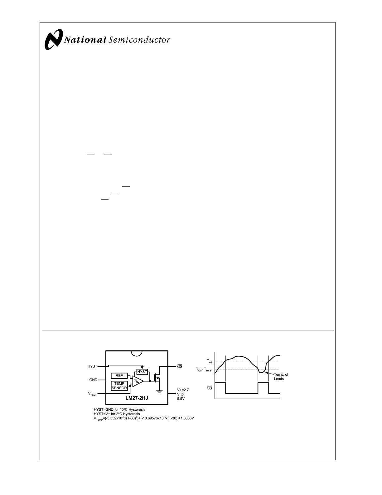
LM27CIM5-2HJ Simplified Block Diagram and Connection Diagram
The LM27CIM5-2HJ has a fixed trip point of 140˚C.
For other trip point and output function availability,
please see ordering information or contact National Semiconductor.
© 2002 National Semiconductor Corporation DS200307 www.national.com
20030701
Page 2
Ordering Information
LM27
For more detailed information on the suffix meaning see the part number template at the end of the Electrical Characteristics Section. Contact National Semiconductor for other set points and output options.
Order Number
Top Mark
LM27CIM5-1HJ LM27CIM5X-1HJ T1HJ MA05B 130˚C Open Drain OS
LM27CIM5-2HJ LM27CIM5X-2HJ T2HJ MA05B 140˚C Open Drain OS
NS Package
Number Trip Point Setting Output FunctionBulk Rail 3000 Units in Tape & Reel
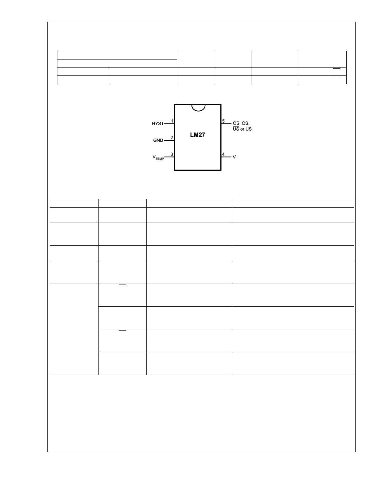
Connection Diagram
20030702
Pin Description
Pin Number Pin Name Function Connection
1 HYST Hysteresis control, digital
input
2 GND Ground, connected to the
back side of the die through
lead frame.
3V
4V
5OS
TEMP
+
OS Overtemperature Shutdown
US
US Undertemperature Shutdown
Analog output voltage
proportional to temperature
Supply input 2.7V to 5.5V with a 0.1µF bypass capacitor.
Overtemperature Shutdown
open-drain active low
thermostat digital output
totem-pull active high
thermostat digital output
Undertemperature Shutdown
open-drain active low
thermostat digital output
totem-pull active high
thermostat digital output
GND for 10˚C or V
System GND
Leave floating or connect to a high impedance
node.
For PSRR information see Section Titled
NOISE CONSIDERATIONS.
Controller interrupt, system or power supply
shutdown; pull-up resistor ≥ 10kΩ
Controller interrupt, system or power supply
shutdown
System or power supply shutdown; pull-up
resistor ≥ 10kΩ
System or power supply shutdown
+
for 2˚C
Note: pin 5 functionality and trip point setting are programmed during LM27 manufacture.
www.national.com 2
Page 3

LM27
Absolute Maximum Ratings (Note 1)
Input Voltage 6.0V
Input Current at any pin (Note 2) 5mA
Package Input Current(Note 2) 20mA
Package Dissipation at T
(Note 3) 500mW
Soldering Information
SOT23 Package
Vapor Phase (60 seconds)
Infrared (15 seconds)
= 25˚C
A
215˚C
220˚C
Storage Temperature −65˚C to + 150˚C
ESD Susceptibility (Note 4)
Human Body Model
2500V
Machine Model
Operating Ratings(Note 1)
Specified Temperature Range T
LM27CIM −40˚C ≤ TA≤ +150˚C
Positive Supply Voltage (V
Maximum V
OUT
+
) +2.7V to +5.5V
MIN
≤ TA≤ T
LM27 Electrical Characteristics
The following specifications apply for V+= 2.7VDCto 5.5VDC, and V
face limits apply for T
A=TJ=TMIN
to T
; all other limits TA=TJ= 25˚C unless otherwise specified.
MAX
Symbol Parameter Conditions (Note 6) Limits (Limits)
Temperature Sensor
<
Trip Point Accuracy (Includes
V
, DAC, Comparator Offset,
REF
+120˚C
<
T
A
and Temperature Sensitivity
errors)
Trip Point Hysteresis HYST = GND 10 ˚C
+
V
Output Temperature
TEMP
HYST = V
Sensitivity
Temperature Sensitivity
V
TEMP
Error to Equation:
= (−3.552x10⁻⁶x(T−30)2+
V
O
(−10.695x10⁻³x(T−30))+
1.8386V
V
Load Regulation −1µA ≤ IL≤ 0 0.070 mV
TEMP
V
Line Regulation +2.7V ≤ V+≤ +5.5V,
TEMP
I
S
Supply Current 15 22
−30˚C ≤ T
2.7V ≤ V
A
+
≤ 5.5V
≤ 150˚C,
−55˚C ≤ TA≤ 150˚C,
+
4.5V ≤ V
T
A
0 ≤ I
−30˚C ≤ T
≤ 5.5V
= 25˚C
≤ +40µA 0.7 mV (max)
L
≤ +120˚C
A
Digital Output and Input
I
OUT(“1”)
Logical “1” Output Leakage
V+= +5.0V 0.001 1 µA (max)
Current (Note 9)
V
OUT(“0”)
V
OUT(“1”)
Logical “0” Output Voltage I
Logical “1” Push-Pull Output
Voltage
V
IH
HYST Input Logical ”1“ Threshold
= +1.2mA and
OUT
+
≥2.7V;
V
= +3.2mA and
I
OUT
+
≥4.5V; (Note 8)
V
I
SOURCE
= 500µA, V
≥ 2.7V
I
SOURCE
V
+
≥4.5V
= 800µA,
Voltage
V
IL
HYST Input Logical ”0“ Threshold
Voltage
load current = 0µA unless otherwise specified. Bold-
TEMP
Typical LM27CIM Units
(Note 7)
+150˚C
±
3 ˚C (max)
2˚C
−10.82 mV/˚C
±
3 ˚C (max)
±
3 ˚C (max)
±
2.5 ˚C (max)
−0.2 mV/V
40
0.4 V (max)
+
+
0.8xV
+
V
− 1.5 V (min)
+
0.8xV
+
0.2xV
µA (max)
µA (max)
V (min)
V (min)
V (max)
250V
MAX
+5.5V
www.national.com3
Page 4

Note 1: Absolute Maximum Ratings indicate limits beyond which damage to the device may occur. Operating Ratings indicate conditions for which the device is
functional, but do not guarantee specific performance limits. For guaranteed specifications and test conditions, see the Electrical Characteristics. The guaranteed
LM27
specifications apply only for the test conditions listed. Some performance characteristics may degrade when the device is not operated under the listed test
conditions.
Note 2: When the input voltage (V
maximum package input current rating limits the number of pins that can safely exceed the power supplies with an input current of 5mA to four. Under normal
operating conditions the maximum current that pins 2, 4 or 5 can handle is limited to 5mA each.
Note 3: The maximum power dissipation must be derated at elevated temperatures and is dictated by T
ambient thermal resistance) and T
given in the Absolute Maximum Ratings, whichever is lower. For this device, T
package types when board mounted follow:
) at any pin exceeds the power supply (V
I
(ambient temperature). The maximum allowable power dissipation at any temperature is PD=(T
A
I
<
Jmax
GND or V
Package Type θ
>
V+), the current at that pin should be limited to 5mA. The 20mA
I
(maximum junction temperature), θJA(junction to
Jmax
= 150˚C. For this device the typical thermal resistance (θJA) of the different
JA
)/θJAor the number
Jmax–TA
SOT23-5, MA05B 250˚C/W
Note 4: The human body model is a 100pF capacitor discharge through a 1.5kΩ resistor into each pin. The machine model is a 200pF capacitor discharged directly
into each pin.
Note 5: See the URL ”http://www.national.com/packaging/“ for other recommendations and methods of soldering surface mount devices.
Note 6: Typicals are at T
Note 7: Limits are guaranteed to National’s AOQL (Average Outgoing Quality Level).
Note 8: Care should be taken to include the effects of self heating when setting the maximum output load current. The power dissipation of the LM27 would increase
by 1.28mW when I
about 0.32˚C due to self heating. Self heating is not included in the trip point accuracy specification.
Note 9: The 1µA limit is based on a testing limitation and does not reflect the actual performance of the part. Expect to see a doubling of the current for every 15˚C
increase in temperature. For example, the 1nA typical current at 25˚C would increase to 16nA at 85˚C.
OUT
= 25˚C and represent most likely parametric norm.
J=TA
=3.2mA and V
=0.4V. With a thermal resistance of 250˚C/W, this power dissipation would cause an increase in the die temperature of
OUT
Part Number Template
The series of digits labeled xyz in the part number LM27CIM-xyz, describe the set point value and the function of the output as
follows:
The place holders xy describe the set point temperature as shown in the following table.
x (10x) y (1x) Temperature (˚C)
-H 0
-J 1
-K 2
-L 3
-N 4
-P 5
-R 6
x (10x) y (1x) Temperature (˚C)
-S 7
-T 8
-V 9
Z- 12
1- 13
2- 14
3- 15
The value of z describes the assignment/function of the output as shown in the following table:
Open-Drain/
Active-Low/High
Push-Pull OS/US Value of z Digital Output Function
0 0 0 J Active-Low, Open-Drain, OS output
0 0 1 K Active-Low, Open-Drain, US output
110LActive-High, Push-Pull, OS output
1 1 1 N Active-High, Push-Pull, US output
For example:
the part number LM27CIM5-2SJ has TOS= 147˚C, and programmed as an active-low open-drain overtemperature shutdown
•
output.
the part number LM27CIM5-ZLN has TUS= 123˚C, and programmed as an active-high, push-pull undertemperature shutdown
•
output.
Active-high open-drain and active-low push-pull options are available, please contact National Semiconductor for more information.
www.national.com 4
Page 5

Functional Description
LM27 OPTIONS
LM27
LM27-_ _J
20030712
LM27-_ _L
20030714
FIGURE 1. Output Pin Options Block Diagrams
The LM27 can be factory programmed to have a trip point
anywhere in-between 120˚C to 150˚C.
Applications Hints
AFTER-ASSEMBLY PCB TESTING
The LM27’s V
by following a simple test procedure. Simply measuring the
output voltage will verify that the LM27 has been
V
TEMP
assembled properly and that its temperature sensing circuitry is functional. The V
capability that can be overdriven by 1.5mA. Therefore, one
can simply force the V
output to change state, thereby verifying that the comparator
and output circuitry function after assembly. Here is a
sample test procedure that can be used to test the
LM27CIM5X-2HJ which has a 140˚C trip point.
1. Turn on V
temperature reading of the LM27 using the equation:
or
2. Verify that the temperature measured in step one is
within (
the ambient/board temperature. The ambient/board temperature (reference temperature) should be measured
using an extremely accurate calibrated temperature sensor, which is in close proximity to and mounted on the
same PCB as the LM27 perhaps even touching the GND
lead of the LM27 if possible. The LM27 will sence the
output allows after-assembly PCB testing
TEMP
output has very weak drive
TEMP
voltage to cause the digital
TEMP
+
and measure V
= (−3.552x10⁻⁶x(T−30)2)+
V
O
(−10.69576x10
±
3˚C + error of reference temperature sensor) of
−3
x(T−30)) + 1.8386V (1)
. Then calculate the
TEMP
(2)
LM27-_ _K
20030713
LM27-_ _N
20030715
board temperature not the ambient temperature (see
Section Titled Mounting Considerations)
3.
A. Observe that OS is high.
B. Drive V
TEMP
to ground.
C. Observe that OS is now low.
D. Release the V
TEMP
pin.
E. Observe that OS is now high.
4.
A. Observe that OS is high.
B. Drive V
C. When OS goes low, note the V
D. V
TEMP
voltage down gradually.
TEMP
Trig=V
at OS trigger (HIGH->LOW)
TEMP
TEMP
voltage.
E. Calculate Ttrig using Equation (2).
5.
A. Gradually raise V
V
.
TEMP
B. Calculate T
V
LOADING
TEMP
The V
output has very weak drive capability (40µA
TEMP
HYST
until OS goes HIGH. Note
TEMP
using Equation (2).
source, 1µA sink). So care should be taken when attaching
circuitry to this pin. Capacitive loading may cause the V
TEMP
output to oscillate. Simply adding a resistor in series as
shown in Figure 2 will prevent oscillations from occurring. To
determine the value of the resistor follow the guidelines
given in Table 1. The same value resistor will work for either
placement of the resistor. If an additional capacitive load is
placed directly on the LM27 output, rather than across
, it should be at least a factor of 10 smaller than
C
LOAD
.
C
LOAD
www.national.com5
Page 6

Applications Hints (Continued)
LM27
TABLE 1. Resistive compensation for capacitive
loading of V
C
LOAD
≤100pF 0
1nF 8200
10nF 3000
100nF 1000
≥1µF 430
a) R in series with capacitor
TEMP
R(Ω)
20030717
MOUNTING CONSIDERATIONS
The LM27 can be applied easily in the same way as other
integrated-circuit temperature sensors. It can be glued or
cemented to a surface. The temperature that the LM27 is
sensing will be within about +0.06˚C of the surface temperature to which the LM27’s leads are attached to.
This presumes that the ambient air temperature is almost the
same as the surface temperature; if the air temperature were
much higher or lower than the surface temperature, the
actual temperature measured would be at an intermediate
temperature between the surface temperature and the air
temperature.
To ensure good thermal conductivity, the backside of the
LM27 die is directly attached to the GND pin (pin 2). The
temperatures of the lands and traces to the other leads of the
LM27 will also affect the temperature that is being sensed.
Alternatively, the LM27 can be mounted inside a sealed-end
metal tube, and can then be dipped into a bath or screwed
into a threaded hole in a tank. As with any IC, the LM27 and
accompanying wiring and circuits must be kept insulated and
dry, to avoid leakage and corrosion. This is especially true if
the circuit may operate at cold temperatures where condensation can occur. Printed-circuit coatings and varnishes such
as Humiseal and epoxy paints or dips are often used to
ensure that moisture cannot corrode the LM27 or its connections.
The junction to ambient thermal resistance (θ
) is the pa-
JA
rameter used to calculate the rise of a part’s junction temperature due to its power dissipation. For the LM27 the
equation used to calculate the rise in the die junction temperature is as follows:
b) R in series with signal path
20030718
FIGURE 2. Resistor placement for capacitive loading
compensation of V
TEMP
NOISE CONSIDERATIONS
The LM27 has excellent power supply noise rejection. Listed
below is a variety of signals used to test the LM27 power
supply rejection. False triggering of the output was not observed when these signals where coupled into the V+ pin of
the LM27.
square wave 400kHz, 1Vp-p
•
square wave 2kHz, 200mVp-p
•
sine wave 100Hz to 1MHz, 200mVp-p
•
Testing was done while maintaining the temperature of the
LM27 one degree centigrade way from the trip point with the
output not activated.
(3)
where T
voltage, I
current on the V
output, and I
is the ambient temperature, V+is the power supply
A
is the quiescent current, I
Q
DO
output, VDOis the voltage on the digital
TEMP
is the load current on the digital output. Since
L_TEMP
is the load
the LM27’s junction temperature is the actual temperature
being measured, care should be taken to minimize the load
current that the LM27 is required to drive.
The tables shown in Figure 3 summarize the thermal resistance for different conditions and the rise in die temperature
of the LM27 without any loading on V
and a 10k pull-up
TEMP
resistor on an open-drain digital output with a 5.5V power
supply.
SOT23-5
no heat sink
θ
JA
(˚C/W)
T
J−TA
(˚C)
SOT23-5
small heat sink
θ
JA
T
(˚C/W)
J−TA
(˚C)
Still Air 250 0.11 TBD TBD
Moving Air TBD TBD TBD TBD
FIGURE 3. Thermal resistance (θ
rise due to self heating (T
) and temperature
JA
J−TA
)
www.national.com 6
Page 7

Typical Applications
LM27
Note: The fan’s control pin has internal pull-up. The 10k pull-down sets a slow fan speed. When the output of the LM27 goes low, the fan will speed up.
20030703
FIGURE 4. Two Speed Fan Speed Control
20030720
FIGURE 5. Fan High Side Drive
FIGURE 6. Fan Low Side Drive
20030721
www.national.com7
Page 8

Typical Applications (Continued)
LM27
20030722
FIGURE 7. Audio Power Amplifier Thermal Protection
FIGURE 8. Simple Thermostat
20030723
www.national.com 8
Page 9

Physical Dimensions inches (millimeters)
unless otherwise noted
LM27 SOT-23,
±
3˚C Accurate, 120˚C-150˚C Factory Preset Thermostat
5-Lead Molded SOT-23 Plastic Package, JEDEC
Order Number LM27CIM5 or LM27CIM5X
NS Package Number MA05B
LIFE SUPPORT POLICY
NATIONAL’S PRODUCTS ARE NOT AUTHORIZED FOR USE AS CRITICAL COMPONENTS IN LIFE SUPPORT
DEVICES OR SYSTEMS WITHOUT THE EXPRESS WRITTEN APPROVAL OF THE PRESIDENT AND GENERAL
COUNSEL OF NATIONAL SEMICONDUCTOR CORPORATION. As used herein:
1. Life support devices or systems are devices or
systems which, (a) are intended for surgical implant
into the body, or (b) support or sustain life, and
whose failure to perform when properly used in
accordance with instructions for use provided in the
2. A critical component is any component of a life
support device or system whose failure to perform
can be reasonably expected to cause the failure of
the life support device or system, or to affect its
safety or effectiveness.
labeling, can be reasonably expected to result in a
significant injury to the user.
National Semiconductor
Corporation
Americas
Email: support@nsc.com
www.national.com
National does not assume any responsibility for use of any circuitry described, no circuit patent licenses are implied and National reserves the right at any time without notice to change said circuitry and specifications.
National Semiconductor
Europe
Fax: +49 (0) 180-530 85 86
Email: europe.support@nsc.com
Deutsch Tel: +49 (0) 69 9508 6208
English Tel: +44 (0) 870 24 0 2171
Français Tel: +33 (0) 1 41 91 8790
National Semiconductor
Asia Pacific Customer
Response Group
Tel: 65-2544466
Fax: 65-2504466
Email: ap.support@nsc.com
National Semiconductor
Japan Ltd.
Tel: 81-3-5639-7560
Fax: 81-3-5639-7507
 Loading...