

Page 1

LM19
2.4V, 10µA, TO-92 Temperature Sensor
General Description
The LM19 is a precision analog output CMOS integratedcircuit temperature sensor that operates over a −55˚C to
+130˚C temperature range. The power supply operating
range is +2.4 V to +5.5 V. The transfer function of LM19 is
predominately linear, yet has a slight predictable parabolic
curvature. The accuracy of the LM19 when specified to a
parabolic transfer function is
ture of +30˚C. The temperature error increases linearly and
reaches a maximum of
extremes. The temperature range is affected by the power
supply voltage. At a power supply voltage of 2.7 V to 5.5 V
the temperature range extremes are +130˚C and −55˚C.
Decreasing the power supply voltage to 2.4 V changes the
negative extreme to −30˚C, while the positive remains at
+130˚C.
The LM19’s quiescent current is less than 10 µA. Therefore,
self-heating is less than 0.02˚C in still air. Shutdown capability for the LM19 is intrinsic because its inherent low power
consumption allows it to be powered directly from the output
of many logic gates or does not necessitate shutdown at all.
±
2.5˚C at an ambient tempera-
±
3.8˚C at the temperature range
Applications
n Cellular Phones
n Computers
n Power Supply Modules
n Battery Management
n FAX Machines
n Printers
n HVAC
n Disk Drives
n Appliances
Features
n Rated for full −55˚C to +130˚C range
n Available in a TO-92 package
n Predictable curvature error
n Suitable for remote applications
Key Specifications
j
Accuracy at +30˚C
j
Accuracy at +130˚C & −55˚C±3.5 to±3.8 ˚C (max)
j
Power Supply Voltage Range +2.4V to +5.5V
j
Current Drain 10 µA (max)
j
Nonlinearity
j
Output Impedance 160 Ω (max)
j
Load Regulation
<
<
I
0µA
+16 µA −2.5 mV (max)
L
January 2003
±
2.5 ˚C (max)
±
0.4 % (typ)
LM19 2.4V, 10µA, TO-92 Temperature Sensor
Typical Application
VO= (−3.88x10⁻⁶xT2) + (−1.15x10⁻²xT) + 1.8639
or
where:
T is temperature, and V
is the measured output voltage of the LM19.
O
FIGURE 1. Full-Range Celsius (Centigrade) Temperature Sensor (−55˚C to +130˚C)
20004002
Operating from a Single Li-Ion Battery Cell
Output Voltage vs Temperature
20004024
© 2003 National Semiconductor Corporation DS200040 www.national.com
Page 2

Typical Application (Continued)
LM19
Connection Diagram
Temperature (T) Typical V
+130˚C +303 mV
+100˚C +675 mV
+80˚C +919 mV
+30˚C +1515 mV
+25˚C +1574 mV
0˚C +1863.9 mV
−30˚C +2205 mV
−40˚C +2318 mV
−55˚C +2485 mV
TO-92
O
See NS Package Number Z03A
20004001
Ordering Information
Order Temperature Temperature NS Package Device
Number Accuracy Range Number Marking Transport Media
LM19CIZ
±
3.8˚C −55˚C to +130˚C Z03A LM19CIZ Bulk
www.national.com 2
Page 3

LM19
Absolute Maximum Ratings (Note 1)
Supply Voltage +6.5V to −0.2V
Output Voltage (V
+
+ 0.6 V) to
Lead Temperature
TO-92 Package
Soldering (3 seconds dwell) +240˚C
−0.6 V
Output Current 10 mA
Input Current at any pin (Note 2) 5 mA
Storage Temperature −65˚C to
+150˚C
Maximum Junction Temperature
(T
) +150˚C
JMAX
ESD Susceptibility (Note 3) :
Operating Ratings(Note 1)
Specified Temperature Range: T
2.4 V ≤ V+≤ 2.7 V −30˚C ≤ TA≤ +130˚C
2.7 V ≤ V
Supply Voltage Range (V
Thermal Resistance, θ
+
≤ 5.5 V −55˚C ≤ TA≤ +130˚C
+
) +2.4 V to +5.5 V
(Note 4)
JA
TO-92 150˚C/W
MIN
≤ TA≤ T
MAX
Human Body Model 2500 V
Machine Model 250 V
Electrical Characteristics
Unless otherwise noted, these specifications apply for V+= +2.7 VDC. Boldface limits apply for TA=TJ=T
other limits T
Parameter Conditions Typical
= 25˚C; Unless otherwise noted.
A=TJ
(Note 5)
LM19C Units
Limits
(Note 6)
Temperature to Voltage Error
= (−3.88x10⁻⁶xT2)
V
O
+ (−1.15x10
−2
xT) + 1.8639V
(Note 7)
= +25˚C to +30˚C
T
A
T
= +130˚C
A
T
= +125˚C
A
T
= +100˚C
A
T
= +85˚C
A
T
= +80˚C
A
T
= 0˚C
A
T
= −30˚C
A
T
= −40˚C
A
T
= −55˚C
A
±
2.5 ˚C (max)
±
3.5 ˚C (max)
±
3.5 ˚C (max)
±
3.2 ˚C (max)
±
3.1 ˚C (max)
±
3.0 ˚C (max)
±
2.9 ˚C (max)
±
3.3 ˚C (min)
±
3.5 ˚C (max)
±
3.8 ˚C (max)
Output Voltage at 0˚C +1.8639 V
Variance from Curve
Non-Linearity (Note 8) −20˚C ≤ T
Sensor Gain (Temperature
−30˚C ≤ T
Sensitivity or Average Slope)
≤ +80˚C
A
≤ +100˚C −11.77 −11.0
A
±
1.0 ˚C
±
0.4 %
−12.6
to equation:
=−11.77 mV/˚CxT+1.860V
V
O
Output Impedance 0 µA ≤ I
≤ +16 µA
L
160 Ω (max)
(Notes 10, 11)
Load Regulation(Note 9) 0 µA ≤ I
≤ +16 µA
L
−2.5 mV (max)
(Notes 10, 11)
Line Regulation +2. 4 V ≤ V+≤ +5.0V +3.7 mV/V (max)
+5.0 V ≤ V
Quiescent Current +2. 4 V ≤ V
+5.0V ≤ V
+2.4V≤ V
Change of Quiescent Current +2. 4 V ≤ V
+
≤ +5.5 V +11 mV (max)
+
≤ +5.0V 4.5 7 µA (max)
+
≤ +5.5V 4.5 9 µA (max)
+
≤ +5.0V 4.5 10 µA (max)
+
≤ +5.5V +0.7 µA
Temperature Coefficient of −11 nA/˚C
Quiescent Current
Shutdown Current V
+
≤ +0.8 V 0.02 µA
to T
MIN
MAX
(Limit)
mV/˚C (min)
mV/˚C (max)
; all
www.national.com3
Page 4

Electrical Characteristics (Continued)
LM19
Note 1: Absolute Maximum Ratings indicate limits beyond which damage to the device may occur. Operating Ratings indicate conditions for which the device is
functional, but do not guarantee specific performance limits. For guaranteed specifications and test conditions, see the Electrical Characteristics. The guaranteed
specifications apply only for the test conditions listed. Some performance characteristics may degrade when the device is not operated under the listed test
conditions.
Note 2: When the input voltage (V
Note 3: The human body model is a 100 pF capacitor discharged through a 1.5 kΩ resistor into each pin. The machine model is a 200 pF capacitor discharged
directly into each pin.
Note 4: The junction to ambient thermal resistance (θ
Note 5: Typicals are at T
Note 6: Limits are guaranteed to National’s AOQL (Average Outgoing Quality Level).
Note 7: Accuracy is defined as the error between the measured and calculated output voltage at the specified conditions of voltage, current, and temperature
(expressed in˚C).
Note 8: Non-Linearity is defined as the deviation of the calculated output-voltage-versus-temperature curve from the best-fit straight line, over the temperature
range specified.
Note 9: Regulation is measured at constant junction temperature, using pulse testing with a low duty cycle. Changes in output due to heating effects can be
computed by multiplying the internal dissipation by the thermal resistance.
Note 10: Negative currents are flowing into the LM19. Positive currents are flowing out of the LM19. Using this convention the LM19 can at most sink −1 µA and
source +16 µA.
Note 11: Load regulation or output impedance specifications apply over the supply voltage range of +2.4V to +5.5V.
Note 12: Line regulation is calculated by subtracting the output voltage at the highest supply input voltage from the output voltage at the lowest supply input voltage.
) at any pin exceeds power supplies (V
I
) is specified without a heat sink in still air.
= 25˚C and represent most likely parametric norm.
J=TA
JA
<
I
GND or V
>
V+), the current at that pin should be limited to 5 mA.
I
Typical Performance Characteristics
Temperature Error vs. Temperature Thermal Response in Still Air
20004034
1.0 LM19 Transfer Function
The LM19’s transfer function can be described in different
ways with varying levels of precision. A simple linear transfer
function, with good accuracy near 25˚C, is
= −11.69 mV/˚C x T + 1.8663 V
V
O
Over the full operating temperature range of −55˚C to
+130˚C, best accuracy can be obtained by using the parabolic transfer function
= (−3.88x10⁻⁶xT2) + (−1.15x10⁻²xT) + 1.8639
V
O
solving for T:
A linear transfer function can be used over a limited temperature range by calculating a slope and offset that give best
results over that range. A linear transfer function can be
calculated from the parabolic transfer function of the LM19.
The slope of the linear transfer function can be calculated
using the following equation:
m = −7.76 x 10
−6
x T − 0.0115,
20004035
where T is the middle of the temperature range of interest
and m is in V/˚C. For example for the temperature range of
T
=−30 to T
min
=+100˚C:
max
T=35˚C
and
m = −11.77 mV/˚C
The offset of the linear transfer function can be calculated
using the following equation:
b=(V
OP(Tmax
)+VOP(T)+mx(T
max
+T))/2
,
where:
VOP(T
•
the parabolic transfer function for V
VOP(T) is the calculated output voltage at T using the
•
parabolic transfer function for V
) is the calculated output voltage at T
max
O
.
O
max
using
Using this procedure the best fit linear transfer function for
many popular temperature ranges was calculated in Figure
2. As shown in Figure 2 the error that is introduced by the
linear transfer function increases with wider temperature
ranges.
www.national.com 4
Page 5

1.0 LM19 Transfer Function (Continued)
LM19
Temperature Range Linear Equation
(˚C) T
T
min
max
(˚C)
V
−55 +130 −11.79 mV/˚C x T + 1.8528 V
−40 +110 −11.77 mV/˚C x T + 1.8577 V
−30 +100 −11.77 mV/˚C x T + 1.8605 V
-40 +85 −11.67 mV/˚C x T + 1.8583 V
−10 +65 −11.71 mV/˚C x T + 1.8641 V
+35 +45 −11.81 mV/˚C x T + 1.8701 V
+20 +30 −11.69 mV/˚C x T + 1.8663 V
FIGURE 2. First Order Equations Optimized For Different Temperature Ranges.
2.0 Mounting
The LM19 can be applied easily in the same way as other
integrated-circuit temperature sensors. It can be glued or
cemented to a surface. The temperature that the LM19 is
sensing will be within about +0.02˚C of the surface temperature to which the LM19’s leads are attached.
This presumes that the ambient air temperature is almost the
same as the surface temperature; if the air temperature were
much higher or lower than the surface temperature, the
actual temperature measured would be at an intermediate
temperature between the surface temperature and the air
temperature.
To ensure good thermal conductivity the backside of the
LM19 die is directly attached to the GND pin. The tempertures of the lands and traces to the other leads of the LM19
will also affect the temperature that is being sensed.
Alternatively, the LM19 can be mounted inside a sealed-end
metal tube, and can then be dipped into a bath or screwed
into a threaded hole in a tank. As with any IC, the LM19 and
accompanying wiring and circuits must be kept insulated and
dry, to avoid leakage and corrosion. This is especially true if
the circuit may operate at cold temperatures where condensation can occur. Printed-circuit coatings and varnishes such
as Humiseal and epoxy paints or dips are often used to
ensure that moisture cannot corrode the LM19 or its connections.
The thermal resistance junction to ambient (θ
rameter used to calculate the rise of a device junction temperature due to its power dissipation. For the LM19 the
equation used to calculate the rise in the die temperature is
as follows:
T
where I
+ θJA[(V+IQ)+(V+−VO)IL]
J=TA
is the quiescent current and ILis the load current on
Q
the output. Since the LM19’s junction temperature is the
actual temperature being measured care should be taken to
minimize the load current that the LM19 is required to drive.
The tables shown in Figure 3 summarize the rise in die
temperature of the LM19 without any loading, and the thermal resistance for different conditions.
) is the pa-
JA
Maximum Deviation of Linear Equation
=
O
from Parabolic Equation (˚C)
±
1.41
±
0.93
±
0.70
±
0.65
±
0.23
±
0.004
±
0.004
TO-92 TO-92
no heat sink small heat fin
θ
JA
TJ−T
θ
A
JA
TJ−T
A
(˚C/W) (˚C) (˚C/W) (˚C)
Still air 150 TBD TBD TBD
Moving air TBD TBD TBD TBD
FIGURE 3. Temperature Rise of LM19 Due to
Self-Heating and Thermal Resistance (θ
)
JA
3.0 Capacitive Loads
The LM19 handles capacitive loading well. Without any precautions, the LM19 can drive any capacitive load less than
300 pF as shown in Figure 4. Over the specified temperature
range the LM19 has a maximum output impedance of 160 Ω.
In an extremely noisy environment it may be necessary to
add some filtering to minimize noise pickup. It is recommended that 0.1 µF be added from V
power supply voltage, as shown in Figure 5. In a noisy
environment it may even be necessary to add a capacitor
from the output to ground with a series resistor as shown in
Figure 5. A 1 µF output capacitor with the 160 Ω maximum
output impedance and a 200 Ω series resistor will form a 442
Hz lowpass filter. Since the thermal time constant of the
LM19 is much slower, the overall response time of the LM19
will not be significantly affected.
FIGURE 4. LM19 No Decoupling Required for
Capacitive Loads Less than 300 pF.
+
to GND to bypass the
20004015
www.national.com5
Page 6

3.0 Capacitive Loads (Continued)
LM19
R(Ω) C (µF)
200 1
470 0.1
680 0.01
1 k 0.001
20004016
20004033
FIGURE 5. LM19 with Filter for Noisy Environment and Capacitive Loading greater than 300 pF. Either placement of
resistor as shown above is just as effective.
4.0 Applications Circuits
FIGURE 6. Centigrade Thermostat
FIGURE 7. Conserving Power Dissipation with Shutdown
www.national.com 6
20004018
20004019
Page 7

4.0 Applications Circuits (Continued)
20004028
Most CMOS ADCs found in ASICs have a sampled data comparator input structure that is notorious for causing grief to analog
output devices such as the LM19 and many op amps. The cause of this grief is the requirement of instantaneous charge of the
input sampling capacitor in the ADC. This requirement is easily accommodated by the addition of a capacitor. Since not all ADCs
have identical input stages, the charge requirements will vary necessitating a different value of compensating capacitor. This ADC
is shown as an example only. If a digital output temperature is required please refer to devices such as the LM74.
FIGURE 8. Suggested Connection to a Sampling Analog to Digital Converter Input Stage
LM19
www.national.com7
Page 8
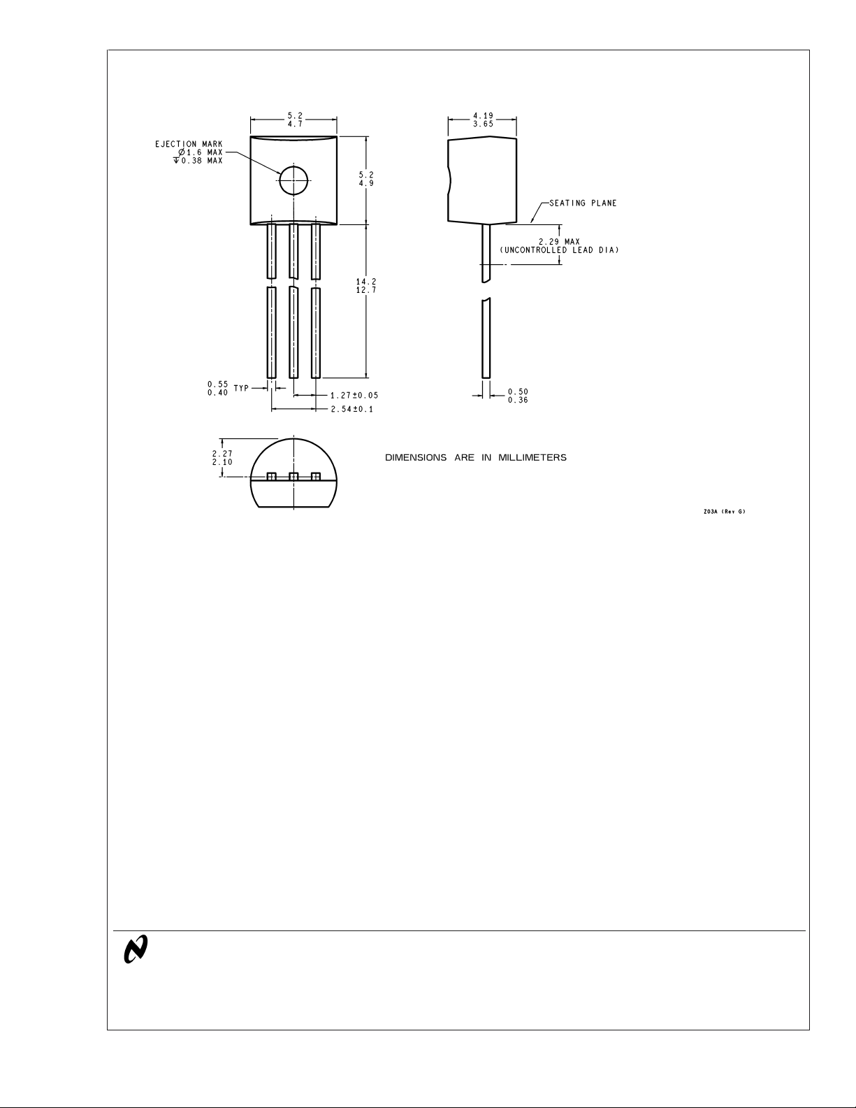
Physical Dimensions inches (millimeters) unless otherwise noted
LM19 2.4V, 10µA, TO-92 Temperature Sensor
3-Lead TO-92 Plastic Package (Z)
Order Number LM19CIZ
NS Package Number Z03A
LIFE SUPPORT POLICY
NATIONAL’S PRODUCTS ARE NOT AUTHORIZED FOR USE AS CRITICAL COMPONENTS IN LIFE SUPPORT
DEVICES OR SYSTEMS WITHOUT THE EXPRESS WRITTEN APPROVAL OF THE PRESIDENT AND GENERAL
COUNSEL OF NATIONAL SEMICONDUCTOR CORPORATION. As used herein:
1. Life support devices or systems are devices or
systems which, (a) are intended for surgical implant
into the body, or (b) support or sustain life, and
whose failure to perform when properly used in
accordance with instructions for use provided in the
labeling, can be reasonably expected to result in a
significant injury to the user.
2. A critical component is any component of a life
support device or system whose failure to perform
can be reasonably expected to cause the failure of
the life support device or system, or to affect its
safety or effectiveness.
National Semiconductor
Americas Customer
Support Center
Email: new.feedback@nsc.com
Tel: 1-800-272-9959
www.national.com
National does not assume any responsibility for use of any circuitry described, no circuit patent licenses are implied and National reserves the right at any time without notice to change said circuitry and specifications.
National Semiconductor
Europe Customer Support Center
Fax: +49 (0) 180-530 85 86
Email: europe.support@nsc.com
Deutsch Tel: +49 (0) 69 9508 6208
English Tel: +44 (0) 870 24 0 2171
Français Tel: +33 (0) 1 41 91 8790
National Semiconductor
Asia Pacific Customer
Support Center
Fax: 65-6250 4466
Email: ap.support@nsc.com
Tel: 65-6254 4466
National Semiconductor
Japan Customer Support Center
Fax: 81-3-5639-7507
Email: nsj.crc@jksmtp.nsc.com
Tel: 81-3-5639-7560
 Loading...