

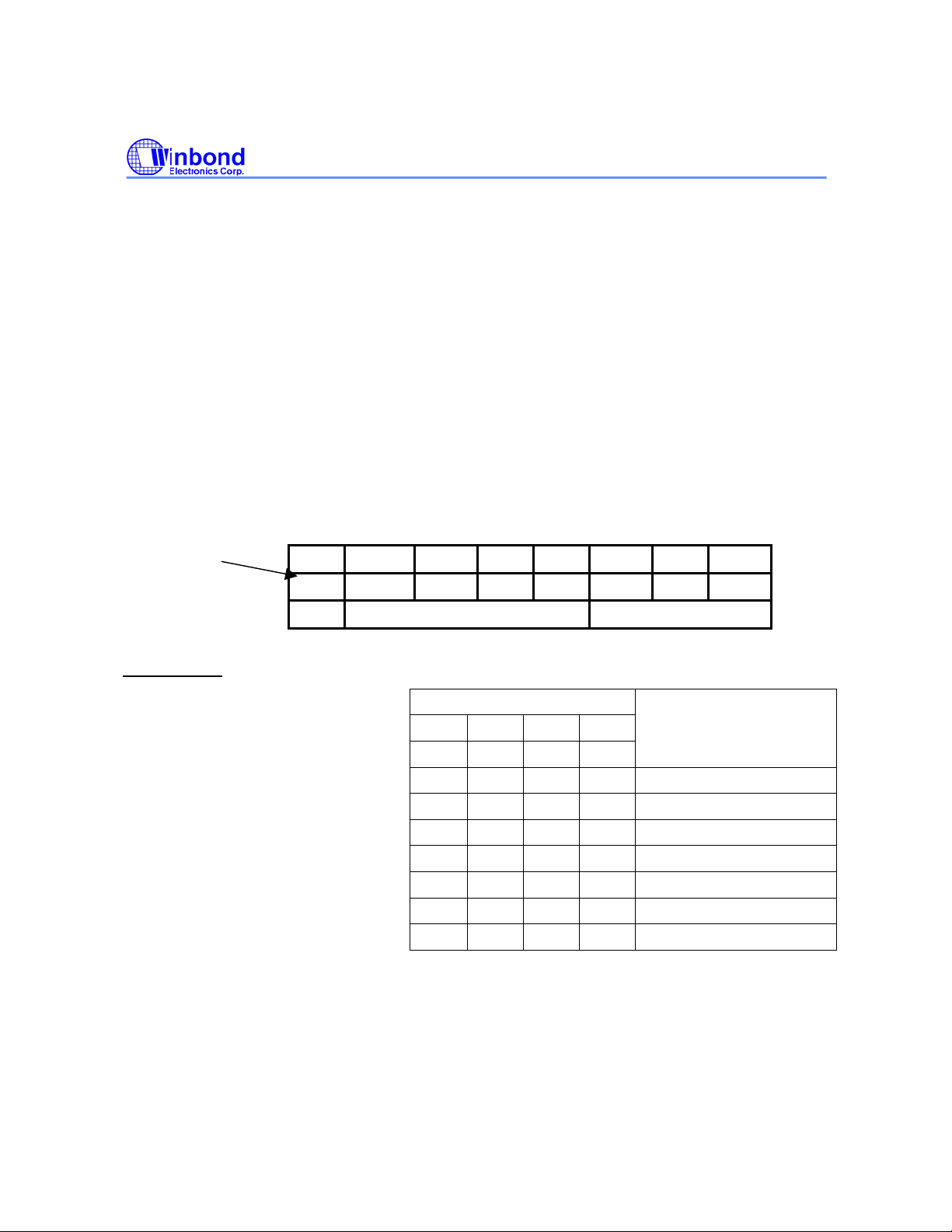
Page 1

PRELIMINARY
ISD5100 SERIES
SINGLE-CHIP
1 TO 16 MINUTES DURATION
VOICE RECORD/PLAYBACK DEVICES
WITH DIGITAL STORAGE CAPABILITY
Publication Release Date: October, 2003
- 1 - Revision 0.2
Page 2

ISD5100 – SERIES
1. GENERAL DESCRIPTION
The ISD5100 ChipCorder
solutions for 1- to 16-minute messaging applications that are ideal for use in cellular phones,
automotive communications, GPS/navigation systems and other portable products. The ISD5100
Series products are an enhancement of the ISD5000 architecture, providing: 1) the I
address, control and duration selection are accomplished through an I
count (ONLY two control lines required); 2) the capability of storing digital data, in addition to analog
data. This feature allows customers to store phone numbers, system configuration parameters and
message address locations for message management capability; 3) Various internal circuit blocks can
be individually powered-up or -down for power saving.
The ISD5100 Series include:
• ISD5116 from 8 to 16 minutes
• ISD5108 from 4 to 8 minutes
• ISD5104 from 2 to 4 minutes
• ISD5102 from 1 to 2 minutes
Analog functions and audio gating have also been integrated into the ISD5100 Series products to
allow easy interface with integrated digital cellular chip sets on the market. Audio paths have been
designed to enable full duplex conversation record, voice memo, answering machine (including
outgoing message playback) and call screening features. This product enables playback of messages
while the phone is in standby, AND both simplex and duplex playback of messages while on a phone
call.
Additional voice storage features for digital cellular phones include: 1) a personalized outgoing
message can be sent to the person by getting caller-ID information from the host chipset, 2) a private
call announce while on call can be heard from the host by giving caller-ID on call waiting information
from the host chipset.
Logic Interface Options of 2.0V and 3.0V are supported by the ISD5100 Series to accommodate
portable communication products (2.0- and 3.0-volt required).
Like other ChipCorder
smoothing filters, and the multi-level storage array on a single-chip. For enhanced voice features, the
ISD5100 Series eliminate external circuitry by integrating automatic gain control (AGC), a power
amplifier/speaker driver, volume control, summing amplifiers, analog switches, and a car kit interface.
Input level adjustable amplifiers are also included, providing a flexible interface for multiple
applications.
Recordings are stored into on-chip nonvolatile memory cells, providing zero-power message storage.
This unique, single-chip solution is made possible through Winbond’s patented multilevel storage
technology. Voice and audio signals are stored directly into solid-state memory in their natural,
uncompressed form, providing superior quality on voice and music reproduction.
Series provide high quality, fully integrated, single-chip Record/Playback
2
2
C interface to minimize pin
®
products, the ISD5100 Series integrate the sampling clock, anti-aliasing and
C serial port -
- 2 -
Page 3

ISD5100 – SERIES
2. FEATURES
Fully-Integrated Solution
• Single-chip voice record/playback solution
• Dual storage of digital and analog data
• Durations
8 to 16-minute (ISD5116)
4 to
2 to
1 to 2-minute (ISD5102)
Low Power Consumption
• +2.7 to +3.3V (VCC) Supply Voltage
• Supports 2.0V and 3.0V interface logic
• Operating Current:
I
I
I
• Standby Current:
ISB = 1µA (typical)
• Most stages can be individually powered down to minimize power consumption
Enhanced Voice Features
• One or two-way conversation record
• One or two-way message playback
• Voice memo record and playback
• Private call screening
• In-terminal answering machine
• Personalized outgoing message
• Private call announce while on call
Digital Memory Features
• Up to 4 Mb available (ISD5116)
• Up to 2 Mb available (ISD5108)
• Up to 1 Mb available (ISD5104)
• Up to 512Kb available (ISD5102)
• Storage of phone numbers, system configuration parameters and message address table in cellular
application
Easy-to-use and Control
• No compression algorithm development required
• User-controllable sampling rates
• Programmable analog interface
• Standard & Fast mode I2C serial interface (100kHz – 400 kHz)
• Fully addressable for multiple messages
High Quality Solution
• High quality voice and music reproduction
• Winbond’s standard 100-year message retention (typical)
• 100K record cycles (typical) for analog data
• 10K record cycles (typical) for digital data
Options
• Available in die form, TSOP and SOIC and PDIP (ISD5116 Only)
• Temperature: Commercial – Packaged (0 to +70°C) & die (0 to +50°C); Industrial (-40 to +85°C)
8-minute (ISD5108)
4-minute (ISD5104)
= 15 mA (typical)
CC Play
= 30 mA (typical)
CC Rec
CC Feedthrough
= 12 mA (typical)
Publication Release Date: October, 2003
- 3 - Revision 0.2
Page 4
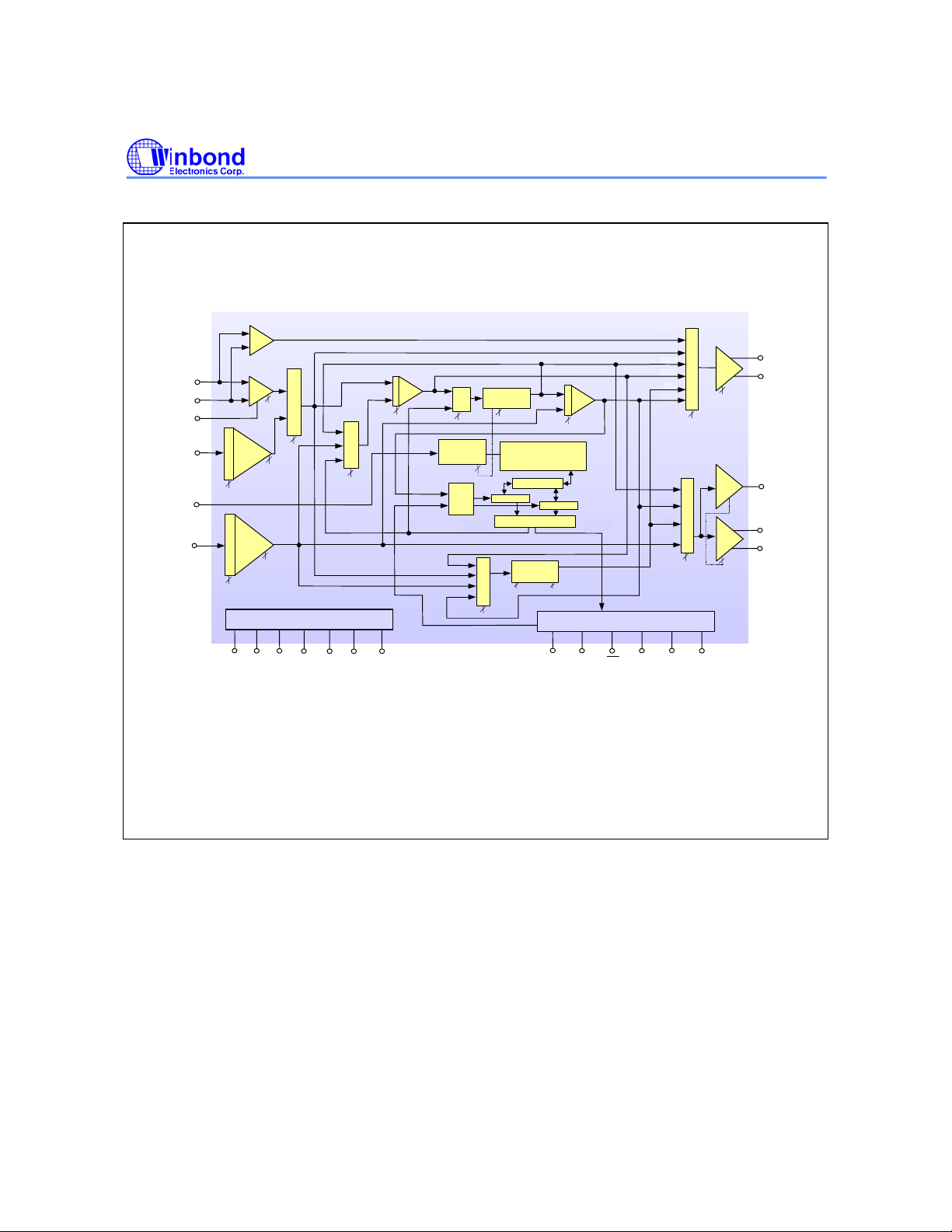
3. BLOCK DIAGRAM
Σ
Σ
ISD5100 – SERIES
MICROPHONE
MIC+
MIC -
AGCCAP
AUX IN
XCLK
ANA IN
ISD5100-Series Block Diagram
6dB
1.0 / 1.4 / 2.0 / 2.8
AUX IN
AMP
AXG0
2 ( )
AXG1
0.625/0.883/1.25/1.76
ANA IN
AMP
2
AIG0
( )
AIG1
V
CCA
Input Source MUX
MIC IN
AGC
1
(AGPD)
AUX IN
1
(INS0)
1
(AXPD)
1
(AIPD)
Power Conditioning
V
V
SSA
SSA
SUM1
Summing
INP
AMP
SUM1 MUX
S1M0
2
( )
S1M1
SUM1 MUX
FILTO
ANA IN
ARRAY
2
S1S0
( )
S1S1
V
V
SSD
V
V
CCD
CCD
SSD
SUM2
(ANALOG)
(DIGITAL)
CTRL
SUM1
ARRAY
MUX
(FLS0)
1
Internal
Clock
FLD0
( )
FLD1
ARRAY
INPUT
MUX
ARRAY OUT
SUM1
INP
ANA IN
SUM2
Low Pass
Filter
2
64-bit/samp.
ARRAY OUTPUT MUX
(ANALOG)
Vol MUX
VLS0
( )
VLS1
2
Filter
FILTO
ANA IN
1
(FLPD)
Multilevel/Digital
Storage Array
Array I/O Mux
64-bit/samp.
Volume
Control
( )
1
3
(V
)
LPD
SCL
2
VOL0
VOL1
VOL2
( )
SUM2
Summing
AMP
S2M0
S2M1
ARRAY OUT
(DIGITAL)
Device Control
FTHRU
ANA OUT MUX
INP
FILTO
SUM1
VOL
SUM2
FILTO
SUM2
VOL
ANA IN
RACINTSDA
3
AOS0
AOS1
( )
AOS2
Output MUX
2
OPS0
( )
OPS1
ANA
OUT
AMP
(AOPD)
AUX
OUT
AMP
Spkr
AMP
( )
A0
A1
1
2
OPA0
OPA1
.
ANA OUT+
ANA OUT-
AUX OUT
SPEAKER
SP+
SP-
- 4 -
Page 5

ISD5100 – SERIES
4. TABLE OF CONTENTS
1. GENERAL DESCRIPTION................................................................................................................... 2
2. FEATURES ..........................................................................................................................................3
3. BLOCK DIAGRAM................................................................................................................................4
4. TABLE OF CONTENTS .......................................................................................................................5
5. PIN CONFIGURATION ........................................................................................................................ 7
6. PIN DESCRIPTION .............................................................................................................................. 8
7. FUNCTIONAL DESCRIPTION.............................................................................................................9
7.1. Overview ........................................................................................................................................9
7.1.1 Speech/Voice Quality...............................................................................................................9
7.1.2. Duration...................................................................................................................................9
7.1.3. Flash Technology....................................................................................................................9
7.1.4. Microcontroller Interface..........................................................................................................9
7.1.5. Programming......................................................................................................................... 10
7.2. Functional Details ........................................................................................................................10
7.2.1. Internal Registers ..................................................................................................................11
7.2.2. Memory Architecture .............................................................................................................11
7.3. Operational Modes Description ...................................................................................................12
7.3.1. I2C Interface ..........................................................................................................................12
7.3.2. I2C Control Registers ............................................................................................................16
7.3.3. Opcode Summary ................................................................................................................. 17
7.3.4. Data Bytes.............................................................................................................................19
7.3.5. Configuration Resiter Bytes ..................................................................................................20
7.3.6. Power-up Sequence..............................................................................................................21
7.3.7. Feed Through Mode..............................................................................................................22
7.3.8. Call Record............................................................................................................................24
7.3.9. Memo Record........................................................................................................................ 25
7.3.10. Memo and Call Playback ....................................................................................................26
7.3.11. Message Cueing .................................................................................................................27
7.4. Analog Mode................................................................................................................................28
7.4.1. Aux In and Ana In Description...............................................................................................28
7.4.2. ISD5100 Series Analog Structure (left half) Description.......................................................29
7.4.3. ISD5100 Series Aanalog Structure (right half) Description ..................................................30
7.4.4. Volume Control Description ..................................................................................................31
7.4.5. Speaker and Aux Out Description......................................................................................... 32
Publication Release Date: October, 2003
- 5 - Revision 0.2
Page 6

ISD5100 – SERIES
7.4.6. Ana Out Description ..............................................................................................................33
7.4.7. Analog Inputs ........................................................................................................................33
7.5. Digital Mode ................................................................................................................................. 36
7.5.1. Erasing Digital Data ..............................................................................................................36
7.5.2. Writing Digital Data ...............................................................................................................36
7.5.3. Reading Digital Data ............................................................................................................. 37
7.5.4. Example Command Sequences ...........................................................................................37
7.6. Pin Details....................................................................................................................................48
7.6.1. Digital I/O Pins.......................................................................................................................48
7.6.2. Analog I/O Pins .....................................................................................................................50
7.6.3. Power and Ground Pins ........................................................................................................ 54
7.6.4. PCB Layout Examples .......................................................................................................... 55
8.1. I2C Timing Diagram......................................................................................................................56
8.2. Playback and Stop Cycle.............................................................................................................58
8.3. Example of Power Up Command (first 12 bits) ...........................................................................59
9. ABSOLUTE MAXIMUM RATINGS.....................................................................................................60
10. ELECTRICAL CHARACTERISTICS ................................................................................................62
10.1. General Parameters ..................................................................................................................62
10.2. Timing Parameters ....................................................................................................................63
10.3. Analog Parameters ....................................................................................................................65
10.4. Characteristics of The I2C Serial Interface ................................................................................69
10.5. I2C Protocol................................................................................................................................72
11. TYPICAL APPLICATION CIRCUIT .................................................................................................. 74
12. PACKAGE SPECIFICATION ...........................................................................................................75
12.1. 28-Lead 8x13.4mm Plastic Thin Small Outline Package (TSOP) Type 1 ................................. 75
12.2. 28-Lead 300-Mil Plastic Small Outline Integrated Circuit (SOIC).............................................. 76
12.3. 28-Lead 600-Mil Plastic Dual Inline Package (PDIP) ................................................................ 77
12.4 ISD5116 Die Information..........................................................................................................78
12.5 ISD5108 Die Information..........................................................................................................80
12.6 ISD5104 Die Information..........................................................................................................82
12.7 ISD5102 Die Information..........................................................................................................84
13. ORDERING INFORMATION............................................................................................................86
14. VERSION HISTORY ........................................................................................................................87
- 6 -
Page 7

5. PIN CONFIGURATION
ISD5100 – SERIES
SCL
A1
SDA
A0
V
SSD
V
SSD
NC
MIC+
V
SSA
MIC-
ANA OUT+
ANA OUT-
ACAP
SP-
1
2
3
4
5
6
7
8
9
10
11
12
13
14
ISD5116
ISD5108
ISD5104
ISD5102
SOIC
NC
V
SSA
RAC
INT
XCLK
V
CCD
V
CCD
SCL
A1
SDA
A0
V
SSD
V
SSD
NC
28
27
26
25
24
23
22
21
20
19
18
17
16
15
1
2
3
4
5
6
7
8
9
10
11
12
13
14
V
CCD
V
CCD
XCLK
INT
RAC
V
SSA
NC
NC
AUX OUT
AUX IN
ANA IN
V
CCA
SP+
V
SSA
ISD5116
ISD5108
ISD5104
ISD5102
SCL
A1
SDA
A0
V
SSD
V
SSD
NC
MIC+
V
SSA
MIC-
ANA OUT+
ANA OUT-
ACAP
SP-
1
2
3
4
5
6
7
8
9
10
11
12
13
14
ISD5116
PDIP
28
27
26
25
24
23
22
21
20
19
18
17
16
15
NC
AUX OU T
AUX IN
ANA IN
V
CCA
SP+
V
SSA
SP-
ACAP
ANA OUT -
ANA OUT +
MIC-
MIC+
V
SSA
28
27
26
25
24
23
22
21
20
19
18
17
16
15
V
CCD
V
CCD
XCLK
INT
RAC
V
SSA
NC
NC
AUX OUT
AUX IN
ANA IN
V
CCA
SP+
V
SSA
TSOP
Publication Release Date: October, 2003
- 7 - Revision 0.2
Page 8
ISD5100 – SERIES
6. PIN DESCRIPTION
Pin Name SOIC/PDIP TSOP Functionality
SCL 1 8 I2C Serial Clock Line: to clock the data into and out of the I2C interface.
A1 2 9 Input pin that supplies the LSB +1 bit for the I2C Slave Address.
SDA 3 10 I2C Serial Data Line: Data is passed between devices on the bus over
this line.
A0 4 11 Input pin that supplies the LSB for the I2C Slave Address.
V
SSD
NC 7,21,22 1,14,28 No Connect.
MIC+ 8 16 Differential Positive Input for the microphone amplifier.
V
SSA
MIC- 10 17 Differential Negative Input for the microphone amplifier.
ANA OUT+ 11 18 Differential Positive Analog Output for ANA OUT.
ANA OUT- 12 19 Differential Negative Analog Output for ANA OUT.
ACAP 13 20 AGC/AutoMute Capacitor: Required for the on-chip AGC amplifier during
SP- 14 21 Differential Negative Speaker Output: When the speaker outputs are in
SP+ 16 23 Differential Positive Speaker Output.
V
CCA
ANA IN 18 25 Analog Input: one of the analog inputs with selectable gain.
AUX IN 19 26 Auxiliary Input: one of the analog inputs with selectable gain.
AUX OUT 20 27 Auxiliary Output: one the analog outputs of the device. When this
RAC 24 3 Row Address Clock; an open drain output. The RAC pin goes LOW
INT
XCLK 26 5 This pin allows the internal clock of the device to be driven externally for
V
CCD
5,6 12,13 Digital Ground.
9,15,23 2,15,22 Analog Ground.
record and AutoMute function during playback.
use, the AUX OUT output is disabled.
17 24 Analog Supply Voltage: This pin supplies power to the analog sections
of the device. It should be carefully bypassed to Analog Ground to
insure correct device operation.
output is used, the SP+ and SP- outputs are disabled.
[1]
before the end of each row of memory and returns HIGH at
T
RACL
exactly the end of each row of memory.
25 4 Interrupt Output; an open drain output that indicates that a set EOM bit
has been found during Playback or that the chip is in an Overflow (OVF)
condition. This pin remains LOW until a Read Status command is
executed.
enhanced timing precision. This pin is grounded for most applications.
27,28 6,7 Digital Supply Voltage. These pins supply power to the digital sections
of the device. They must be carefully bypassed to Digital Ground to
insure correct device operation.
[1]
See the Parameters section
- 8 -
Page 9
ISD5100 – SERIES
7. FUNCTIONAL DESCRIPTION
7.1. OVERVIEW
7.1.1 Speech/Voice Quality
The ISD5100 ChipCorder Series can be configured via software to operate at 4.0, 5.3, 6.4 or 8.0 kHz
sampling frequency to select appropriate voice quality. Increasing the duration decreases the
sampling frequency and bandwidth, which affects audio quality. The table in the following section
shows the relationship between sampling frequency, duration and filter pass band.
7.1.2. Duration
To meet system requirements, the ISD5100 Series are single-chip solution, which provide 1 to 16
minutes of voice record and playback, depending upon the sample rates chosen.
Sample Rate
(kHz)
8.0 8 min 44 sec 4 min 22 sec 2 min 11 sec 1 min 5 sec 3.4
6.4 10 min 55 sec 5 min 27 sec 2 min 43 sec 1 min 21 sec 2.7
5.3 13 min 6 sec 6 min 33 sec 3 min 17 sec 1 min 38 sec 2.3
4.0 17 min 28 sec 8 min 44 sec 4 min 22 sec 2 min 11 sec 1.7
Duration
ISD5116 ISD5108 ISD5104 ISD5102
[1]
Minus any pages selected for digital storage
[1]
Typical Filter
Knee (kHz)
7.1.3. Flash Technology
One of the benefits of Winbond’s ChipCorder technology is the use of on-chip Flash memory, which
provides zero-power message storage. The message is retained for up to 100 years (typically) without
power. In addition, the device can be re-recorded over 10,000 times (typically) for the digital data and
over 100,000 times (typically) for the analog messages.
A new feature has been added that allows memory space in the ISD5100 Series to be allocated to
either digital or analog storage when recorded. The fact that a section has been assigned digital or
analog data is stored in the Message Address Table by the system microcontroller when the recording
is made.
7.1.4. Microcontroller Interface
The ISD5100 Series are controlled through an I
allows commands, configurations, address data, and digital data to be loaded into the device, while
allowing status, digital data and current address information to be read back from the device. In
addition to the serial interface, two other status pins can feedback to the microcontroller for enhanced
- 9 - Revision 0.2
2
C 2-wire interface. This synchronous serial port
Publication Release Date: October, 2003
Page 10
ISD5100 – SERIES
A
interface. These are the
Communications with all the internal registers of any operations are through the serial bus, as well as
digital memory Read and Write operations.
7.1.5. Programming
The ISD5100 Series are also ideal for playback-only applications, where single or multiple messages
may be played back when desired. Playback is controlled through the I
message configuration is created, duplicates can easily be generated via a third-party programmer.
For more information on available application tools and programmers, please see the Winbond web
site at www.winbond-usa.com
RAC timing pin and the INT pin for interrupts to the controller.
2
C interface. Once the desired
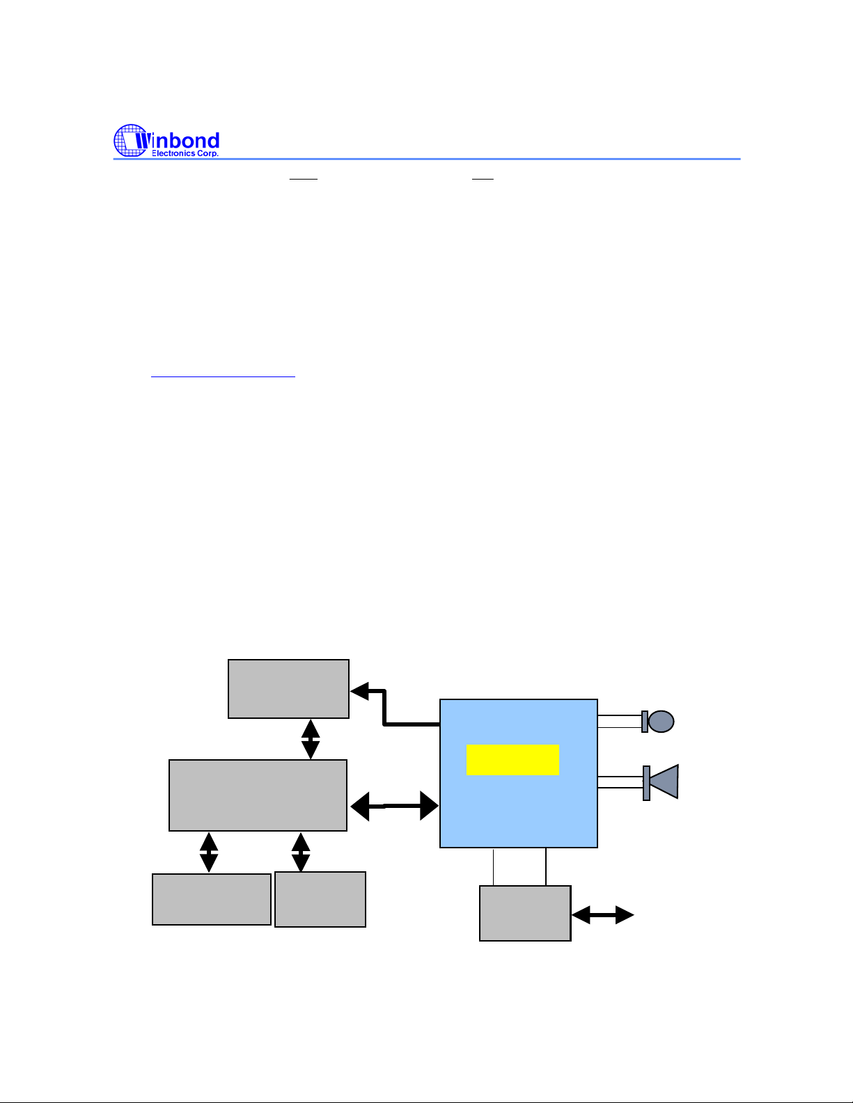
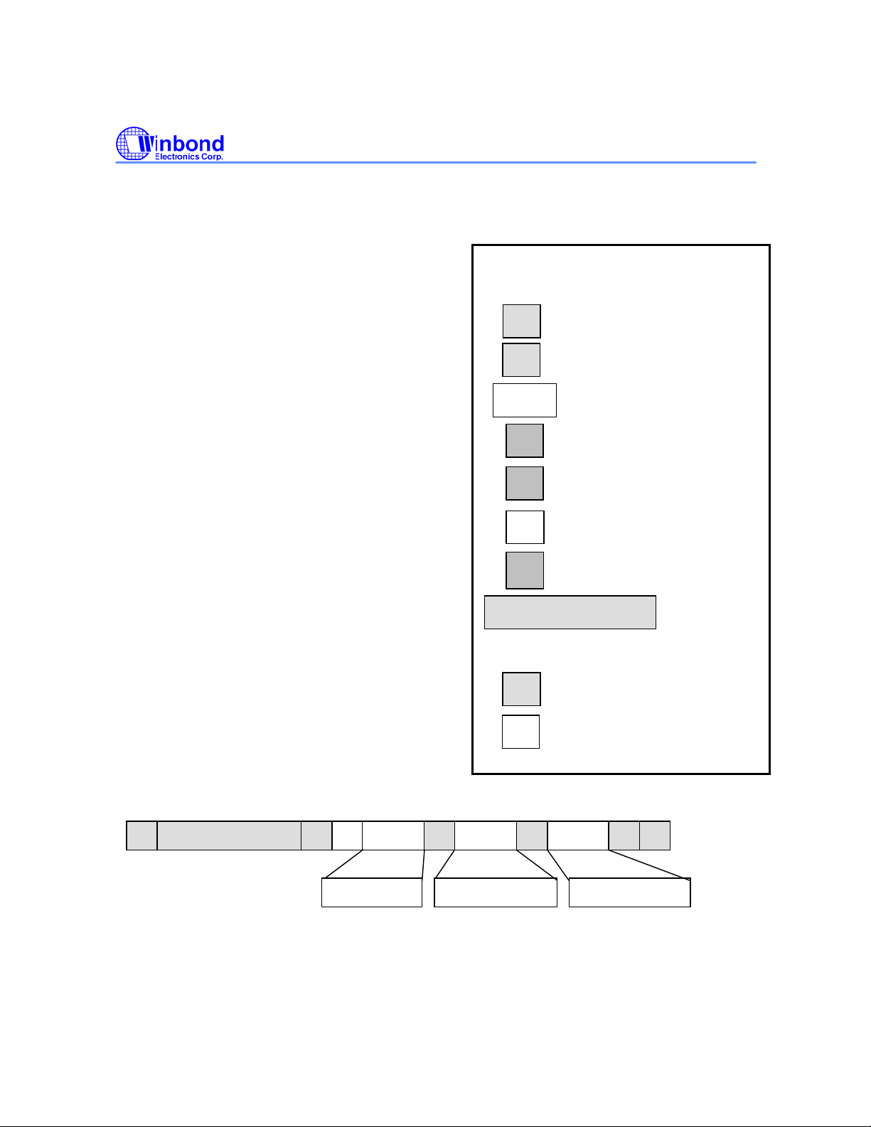
7.2. FUNCTIONAL DETAILS
The ISD5100 Series are single chip solutions for analog and digital data storage. The array can be
divided between analog and digital storage according to user’s choice, when the device is configured.
The below block diagram shows that the ISD5116 device can be easily designed into a telephone
answering machine (TAD). Both Mic inputs transmit the voice input signal from the microphone to
perform OGM recording, as well as to record the speech during phone conversation (simplex).
When the TAD is activated, the voice of the other party from the phone line feeds into the AUX IN, and
is recorded into the ISD5116 device. Then the new messge is usually indicated with blinking new
message LED. Hence, during playback, the recorded message is sent out to speaker with volume
control. Two I
microcontroller for analog and/or digital storage, and the two outputs, INT and RAC are feedback to
microcontroller for message management.
For duplex recording, speech from Mic inputs and message from received path can be directly
recorded into the array simultaneously, then playback afterwards. In addition, for speaker phone
Display &
Push buttons
2
C pins are used for all communications between the ChipCorder and the
DTMF Detect,
Caller ID
Microcontroller
Memory
NV
I2C
(INT, RAC)
NA OUT+
ISD5116
AUX IN AUX OUT
MIC+
MIC-
SP+
SP-
Speaker
Phone Line
- 10 -
Page 11
ISD5100 – SERIES
operation, voice from Mic inputs are fed to AUX OUT and transmitted to the phone line, while
message from other party is input from the AUX IN, then fed through to the speaker for listening.
The ISD5100 device has the flexibility for other applications, because the audio paths can be
configured differently, with each circuit block being powered-up or –down individually, according to the
applications requirement.
7.2.1. Internal Registers
The ISD5100 Series have multiple internal registers that are used to store the address information and
the configuration or set-up of the device. The two 16-bit configuration registers control the audio paths
through the device, the sample frequency, the various gains and attenuations, power up and down of
different sections, and the volume settings. These registers are discussed in detail in section 7.3.5
7.2.2. Memory Architecture
The ISD5100 Series memory array are arranged in various pages (or rows) of each 2048 bits as
follows. The primary addressing for the pages are handled by 11 bits of address input in the analog
mode.
A memory page is 2048 bits organized as thirty-two 64-bit "blocks" when used for digital storage. The
contents of a page are either analog or digital. This is determined by instruction (opcode) at the time
the data is written. A record of where is analog and where is digital, is stored in a message address
table (MAT) by the system microcontroller. The MAT is a table kept in the microcontroller memory that
defines the status of each message “page”. It can be stored back into the ISD5100 Series if the power
fails or the system is turned off. Using this table allows efficient message management. Segments of
messages can be stored wherever there is available space in the memory array. [This is explained in
detail for the ISD5008 in Applications Note #9 and will be similarly described in a later Note for the
ISD5100-Series.]
Products Pages (Rows) Bits/Page Memory Size
ISD5116 2048 2048 4,194,304 bits
ISD5108 1024 2048 2,097,152 bits
ISD5104 512 2048 1,048,576 bits
ISD5102 256 2048 524,288 bits
When a page is used for analog storage, the same 32 blocks are present but there are 8 EOM (Endof-Message) markers. This means that for each 4 blocks there is an EOM marker at the end. Thus,
when recording, the analog recording will stop at any one of eight positions. At 8 kHz sampling
frequency, this results in a resolution of 32 msec when ENDING an analog recording. Beginning an
analog recording is limited to the 256 msec resolution provided by the 11-bit address. A recording
does not immediately stop when the Stop command is given, but continues until the 32 millisecond
block is filled. Then a bit is placed in the EOM memory to develop the interrupt that signals a
message is finished playing in the Playback mode.
.
Publication Release Date: October, 2003
- 11 - Revision 0.2
Page 12

ISD5100 – SERIES
Digital data is sent and received serially over the I
and stored in one of two alternating (commutating) 64-bit shift registers. When an input register is full,
it becomes the register that is parallel written into the array. The prior write register becomes the new
serial input register. A mechanism is built-in to ensure there is always a register available for storing
new data.
Storing data in the memory is accomplished by accepting data one byte at a time and issuing an
acknowledge. If data is coming in faster than it can be written, the chip issues an acknowledge to the
host microcontroller, but holds SCL LOW until it is ready to accept more data. (See section 7.5.2 for
details).
The read mode is the opposite of the write mode. Data is read into one of two 64-bit registers from the
array and serially sent to the I
2
C interface. (See section 7.5.3 for details).
7.3. OPERATIONAL MODES DESCRIPTION
2
C interface. The data is serial-to-parallel converted
7.3.1. I2C Interface
To use more than four ISD5100 Series devices in an application requires some external switching of
2
the I
C interface.
2
I
C interface
Important note: The rest of this data sheet will assume that the reader is familiar with the
2
C serial interface. Additional information on I2C may be found in section 10 on page 72 of
I
this document. If you are not familiar with this serial protocol, please read this section to
familiarize yourself with it. A large amount of additional information on I
found on the Philips web page at http://www.philips.com/
2
I
C Slave Address
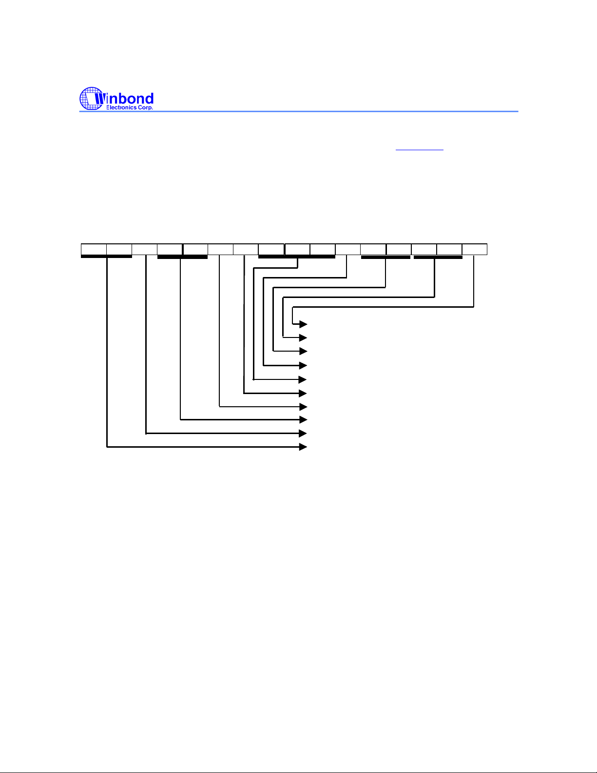
The ISD5100 Series have 7-bit slave address of <100 00xy> where x and y are equal to the state,
respectively, of the external address pins A1 and A0. Because all data bytes are required to be 8
bits, the LSB of the address byte is the Read/Write selection bit that tells the slave whether to transmit
or receive data. Therefore, there are 8 possible slave addresses for the ISD5100-Series. These
are:
.
2
C can also be
- 12 -
Page 13
ISD5100 – SERIES
Pinout Table
A1 A0 Slave
Address
0 0 <100 0000> 0 80
0 1 <100 0001> 0 82
1 0 <100 0010> 0 84
1 1 <100 0011> 0 86
0 0 <100 0000> 1 81
0 1 <100 0001> 1 83
1 0 <100 0010> 1 85
1 1 <100 0011> 1 87
ISD5100 Series I
There are many control functions used to operate the ISD5100-Series. Among them are:
7.3.1.1. Read Status Command:
The Read Status command is a read request from the Host processor to the ISD5100 Series
without delivering a Command Byte. The Host supplies all the clocks (SCL). In each case, the
entity sending the data drives the data line (SDA). The Read Status Command is executed by the
following I
1. Host executes I
2. Send Slave Address with R/W bit = “1” (Read) 81h
3. Slave (ISD5100-Series) responds back to Host an Acknowledge (ACK) followed by 8-bit
Status word
4. Host sends an Acknowledge (ACK) to Slave
5. Wait for SCL to go HIGH
6. Slave responds with Upper Address byte of internal address register
7. Host sends an ACK to Slave
8. Wait for SCL to go HIGH
9. Slave responds with Lower Address byte of internal address register (A[4:0] will always return
set to 0.)
10. Host sends a NO ACK to Slave, then executes I
2
C Operation Definitions
2
C sequence.
2
C START
R/W Bit
2
C STOP
HEX Value
Publication Release Date: October, 2003
- 13 - Revision 0.2
Page 14
Note that the processor could have sent an I
A
A
R
A
2
C STOP
after the Status Word data transfer and aborted the
transfer of the Address bytes.
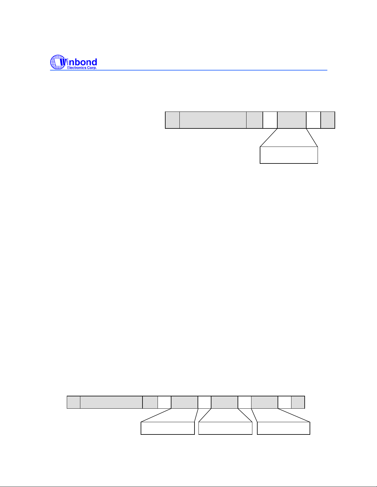
A graphical representation of this operation is found
below. See the caption box above for more
explanation.
S SLAVE ADDRESS
DATA P
Status
High Addr.
ISD5100 – SERIES
Conventions used in I2C Data
Transfer Diagrams
S
= START Condition
= STOP Condition
P
= 8-bit data transfer
DATA
R
= “1” in the R/W bit
= “0” in the R/W bit
W
A
= ACK (Acknowledge)
= No ACK
N
SLAVE ADDRESS
The Box color indicates the direction
of data flow
= Host to Slave (Gray)
=
DATADATA
N
Low Addr.
= 7-bit Slave
Address
- 14 -
Page 15
ISD5100 – SERIES
A
A
A
A
7.3.1.2. Load Command Byte Register (Single Byte Load):
A single byte may be written to the Command Byte Register in order to power up the device, start
or stop Analog Record (if no address information is needed), or do a Message Cueing function.
The Command Byte Register is loaded as follows:
1. Host executes I
2. Send Slave Address with R/W bit = “0” (Write) [80h]
3. Slave responds back with an ACK.
4. Wait for SCL to go HIGH
5. Host sends a command byte to Slave
6. Slave responds with an ACK
7. Wait for SCL to go HIGH
8. Host executes I
7.3.1.3. Load Command Byte Register (Address Load)
For the normal addressed mode the Registers are loaded as follows:
1. Host executes I
2. Send Slave Address with R/W bit = “0” (Write)
3. Slave responds back with an ACK.
4. Wait for SCL to go HIGH
5. Host sends a byte to Slave - (Command Byte)
6. Slave responds with an ACK
7. Wait for SCL to go HIGH
8. Host sends a byte to Slave - (High Address Byte)
9. Slave responds with an ACK
10. Wait for SCL to go HIGH
11. Host sends a byte to Slave - (Low Address Byte)
12. Slave responds with an ACK
13. Wait for SCL to go HIGH
14. Host executes I
S SLAVE ADDRESS
2
C START
2
C STOP
2
C START
2
C STOP
S SLAVE ADDRESS A DATA PW
DATA
DATA
Command Byte
DATA
PW
A
Command
- 15 - Revision 0.2
High Addr. Low Addr.
Publication Release Date: October, 2003
Page 16
ISD5100 – SERIES
2
7.3.2. I
The ISD5100 Series are controlled by loading commands to, or, reading from, the internal command,
configuration and address registers. The Command byte sent is used to start and stop recording, write
or read digital data and perform other functions necessary for the operation of the device.
Command Byte
Control of the ISD5100 Series are implemented through an 8-bit command byte, sent after the 7-bit
device address and the 1-bit Read/Write selection bit. The 8 bits are:
Power Up
Bit
C Control Registers
Global power up bit
DAB bit: determines whether device is performing an analog or digital function
3 function bits: these determine which function the device is to perform in conjunction
with the DAB bit.
3 register address bits: these determine if and when data is to be loaded to a register
C7 C6 C5 C4 C3 C2 C1 C0
PU DAB FN2 FN1 FN0 RG2 RG1 RG0
Function Bits Register Bits
Function Bits
The command byte function bits are
detailed in the table to the right. C6, the
DAB bit, determines whether the
device is performing an analog or
digital function. The other bits are
decoded to produce the individual
commands. Not all decode
combinations are currently used, and
are reserved for future use. Out of 16
possible codes, the ISD5100 Series
uses 7 for normal operation. The other
9 are undefined
Function Bits
C6 C5 C4 C3
DAB FN2 FN1 FN0
0 0 0 0 STOP (or do nothing)
0 1 0 1 Analog Play
0 0 1 0 Analog Record
0 1 1 1 Analog MC
1 1 0 0 Digital Read
1 0 0 1 Digital Write
1 0 1 0 Erase (row)
Function
- 16 -
Page 17
ISD5100 – SERIES
Register Bits
The register load may be used to modify a command
sequence (such as load an address) or used with the null
command sequence to load a configuration or test
register. Not all registers are accessible to the user. [RG2
is always 0 as the four additional combinations are
undefined.]
OpCode Command Description
The following commands are used to access the chip through the I
Play: analog play command
Record: analog record command
Message Cue: analog message cue command
Read: digital read command
Write: digital write command
Erase: digital page and block erase command
Power up: global power up/down bit. (C7)
Load CFG0: load configuration register 0
Load CFG1: load configuration register 1
Read STATUS: Read the interrupt status and address register, including a hardwired device ID
7.3.3. Opcode Summary
RG2 RG1 RG0
C2 C1 C0
0 0 0 No action
0 0 1 Reserved
0 1 0 Load CFG0
0 1 1 Load CFG1
2
C interface.
Function
Publication Release Date: October, 2003
- 17 - Revision 0.2
Page 18

ISD5100 – SERIES
OPCODE COMMAND BYTE TABLE
Pwr Function Bits Register Bits
OPCODE HEX PU DAB FN2 FN1 FN0 RG2 RG1 RG0
COMMAND BIT NUMBER CMD C7 C6 C5 C4 C3 C2 C1 C0
POWER UP 80 1 0 0 0 0 0 0 0
POWER DOWN 00 0 0 0 0 0 0 0 0
STOP (DO NOTHING) STAY ON 80 1 0 0 0 0 0 0 0
STOP (DO NOTHING) STAY OFF 00 0 0 0 0 0 0 0 0
LOAD CFG0 82 1 0 0 0 0 0 1 0
LOAD CFG1 83 1 0 0 0 0 0 1 1
RECORD ANALOG 90 1 0 0 1 0 0 0 0
RECORD ANALOG @ ADDR 91 1 0 0 1 0 0 0 1
PLAY ANALOG A8 1 0 1 0 1 0 0 0
PLAY ANALOG @ ADDR A9 1 0 1 0 1 0 0 1
MSG CUE ANALOG B8 1 0 1 1 1 0 0 0
MSG CUE ANALOG @ ADDR B9 1 0 1 1 1 0 0 1
ENTER DIGITAL MODE
EXIT DIGITAL MODE 40 0 1 0 0 0 0 0 0
DIGITAL ERASE PAGE D0 1 1 0 1 0 0 0 0
DIGITAL ERASE PAGE @ ADDR D1 1 1 0 1 0 0 0 1
DIGITAL WRITE C8 1 1 0 0 1 0 0 0
DIGITAL WRITE @ ADDR C9 1 1 0 0 1 0 0 1
DIGITAL READ E0 1 1 1 0 0 0 0 0
DIGITAL READ @ ADDR E1 1 1 1 0 0 0 0 1
READ STATUS1 N/A N/A N/A N/A N/A N/A N/A N/A N/A
1. See section 7.2 on page 12 for details.
C0 1 1 0 0 0 0 0 0
- 18 -
Page 19
ISD5100 – SERIES
7.3.4. Data Bytes
2
In the I
option is selected, the next two bytes are loaded into the selected register. The format of the data is
MSB first, the I
byte is acknowledged, and DATA<7:0> is sent next. The address register consists of two bytes. The
format of the address is as follows:
ADDRESS<15:0> = PAGE_ADDRESS<10:0>, BLOCK_ADDRESS<4:0>
Note: if an analog function is selected, the block address bits must be set to 00000. Digital
Read and Write are block addressable.
When the device is polled with the Read Status command, it will return three bytes of data. The first
byte is the status byte, the next the upper address byte and the last the lower address byte. The status
register is one byte long and its bit function is:
STATUS<7:0> = EOM, OVF, READY, PD, PRB, DEVICE_ID<2:0>
Lower address byte will always return the block address bits as zero, either in digital or analog mode.
The functions of the bits are:
EOM BIT 7 Indicates whether an EOM interrupt has occurred.
OVF BIT 6 Indicates whether an overflow interrupt has occurred.
READY BIT 5 Indicates the internal status of the device – if READY is LOW
PD BIT 4 Device is powered down if PD is HIGH.
PRB BIT 3 Play/Record mode indicator. HIGH=Play/LOW=Record.
DEVICE_ID BIT 0, 1, 2 An internal device ID. ISD5116 = 001; ISD5108 = 010;
It is recommended that you read the status register after a Write or Record operation to ensure that
the device is ready to accept new commands. Depending upon the design and the number of pins
available on the controller, the polling overhead can be reduced. If
microcontroller, it does not have to poll as frequently to determine the status of the ISD5100-SERIES.
C write mode, the device can accept data sent after the command byte. If a register load
2
C standard. Thus to load DATA<15:0> into the device, DATA<15:8> is sent first, the
no new commands should be sent to device, i.e. Not Ready.
ISD5104 = 100 and ISD5102 = 101.
INT and RAC are tied to the
Publication Release Date: October, 2003
- 19 - Revision 0.2
Page 20
ISD5100 – SERIES
7.3.5. Configuration Resiter Bytes
The configuration register bytes are defined, in detail, in the drawings of section 7.4
drawings display how each bit enables or disables a function of the audio paths in the ISD5100Series. The tables below give a general illustration of the bits. There are two configuration registers,
CFG0 and CFG1, so there are four 8-bit bytes to be loaded during the set-up of the device.
Configuration Register 0 (CFG0)
Configuration Register 0 (CFG0)
D15 D14 D13 D12 D11 D10 D9 D8 D7 D 6 D5 D4 D3 D2 D1 D0
D15 D14 D13 D12 D11 D10 D9 D8 D7 D 6 D5 D4 D3 D2 D1 D0
AIG1 AIG0 AIPD AXG1 AXG0 AXPD INS0 AOS2 AOS1 AOS0 AOPD OPS1 OPS0 OPA1 OPA0 VLPD
AIG1 AIG0 AIPD AXG1 AXG0 AXPD INS0 AOS2 AOS1 AOS0 AOPD OPS1 OPS0 OPA1 OPA0 VLPD
Volume Control Power Down
Volume Control Power Down
SPKR & AUX OUT Control (2 bits)
SPKR & AUX OUT Control (2 bits)
OUTPUT MUX Select (2 bits)
OUTPUT MUX Select (2 bits)
ANA OUT Power Down
ANA OUT Power Down
AUXOUT MUX Select (3 bits)
AUXOUT MUX Select (3 bits)
INPUT SOURCE MUX Select (1 bit)
INPUT SOURCE MUX Select (1 bit)
AUX IN Power Down
AUX IN Power Down
AUX IN AMP Gain SET (2 bits)
AUX IN AMP Gain SET (2 bits)
ANA IN Power Down
ANA IN Power Down
ANA IN AMP Gain SET (2 bits)
ANA IN AMP Gain SET (2 bits)
on page 29. The
- 20 -
Page 21
ISD5100 – SERIES
Configuration Register 1 (CFG1)
Configuration Register 1 (CFG1)
D15 D14 D13 D12 D11 D10 D9 D8 D7 D 6 D5 D4 D3 D2 D1 D0
D15 D14 D13 D12 D11 D10 D9 D8 D7 D 6 D5 D4 D3 D2 D1 D0
D15 D14 D13 D12 D11 D10 D9 D8 D7 D 6 D5 D4 D3 D2 D1 D0
D15 D14 D13 D12 D11 D10 D9 D8 D7 D 6 D5 D4 D3 D2 D1 D0
VLS1 VLS0 VOL2 VOL1 VOL0 S1S1 S1S0 S1M1 S1M0 S2M1 S2M0 FLS0 FLD1 FLD0 FLPD AGPD
VLS1 VLS0 VOL2 VOL1 VOL0 S1S1 S1S0 S1M1 S1M0 S2M1 S2M0 FLS0 FLD1 FLD0 FLPD AGPD
VLS1 VLS0 VOL2 VOL1 VOL0 S1S1 S1S0 S1M1 S1M0 S2M1 S2M0 FLS0 FLD1 FLD0 FLPD AGPD
VLS1 VLS0 VOL2 VOL1 VOL0 S1S1 S1S0 S1M1 S1M0 S2M1 S2M0 FLS0 FLD1 FLD0 FLPD AGPD
AGC AMP Power Down
AGC AMP Power Down
Filter Power Down
Filter Power Down
SAMPLE RATE (& Filter) Set up (2 bits)
SAMPLE RATE (& Filter) Set up (2 bits)
FILTER MUX Select
FILTER MUX Select
SUM 2 SUMMING AMP Control (2 bits)
SUM 2 SUMMING AMP Control (2 bits)
SUM 1 SUMMING AMP Control (2 bits)
SUM 1 SUMMING AMP Control (2 bits)
SUM 1 MUX Select (2 bits)
SUM 1 MUX Select (2 bits)
VOLUME CONTROL (3 bits)
VOLUME CONTROL (3 bits)
VOLUME CONT. MUX Select (2 bits)
VOLUME CONT. MUX Select (2 bits)
7.3.6. Power-up Sequence
This sequence prepares the ISD5100 Series for an operation to follow, waiting the Tpud time before
sending the next command sequence.
1. Send I
2. Send one byte 10000000 {Slave Address, R/W = 0} 80h
3. Slave ACK
4. Wait for SCL High
5. Send one byte 10000000 {Command Byte = Power Up} 80h
6. Slave ACK
7. Wait for SCL High
8. Send I
Playback Mode
The command sequence for an analog Playback operation can be handled several ways. The most
straightforward approach would be to incorporate a single four byte exchange, which consists of the
Slave Address (80h), the Command Byte (A9h) for Play Analog @ Address, and the two address
bytes.
2
C POWER UP
2
C STOP
Publication Release Date: October, 2003
- 21 - Revision 0.2
Page 22
ISD5100 – SERIES
A
p
r
A
O
V
Record Mode
The command sequence for an Analog Record would be a four byte sequence consisting of the Slave
Address (80h), the Command Byte (91h) for Record Analog @ Address, and the two address bytes.
See “Load Command Byte Register (Address Load)” in section 7.3.2
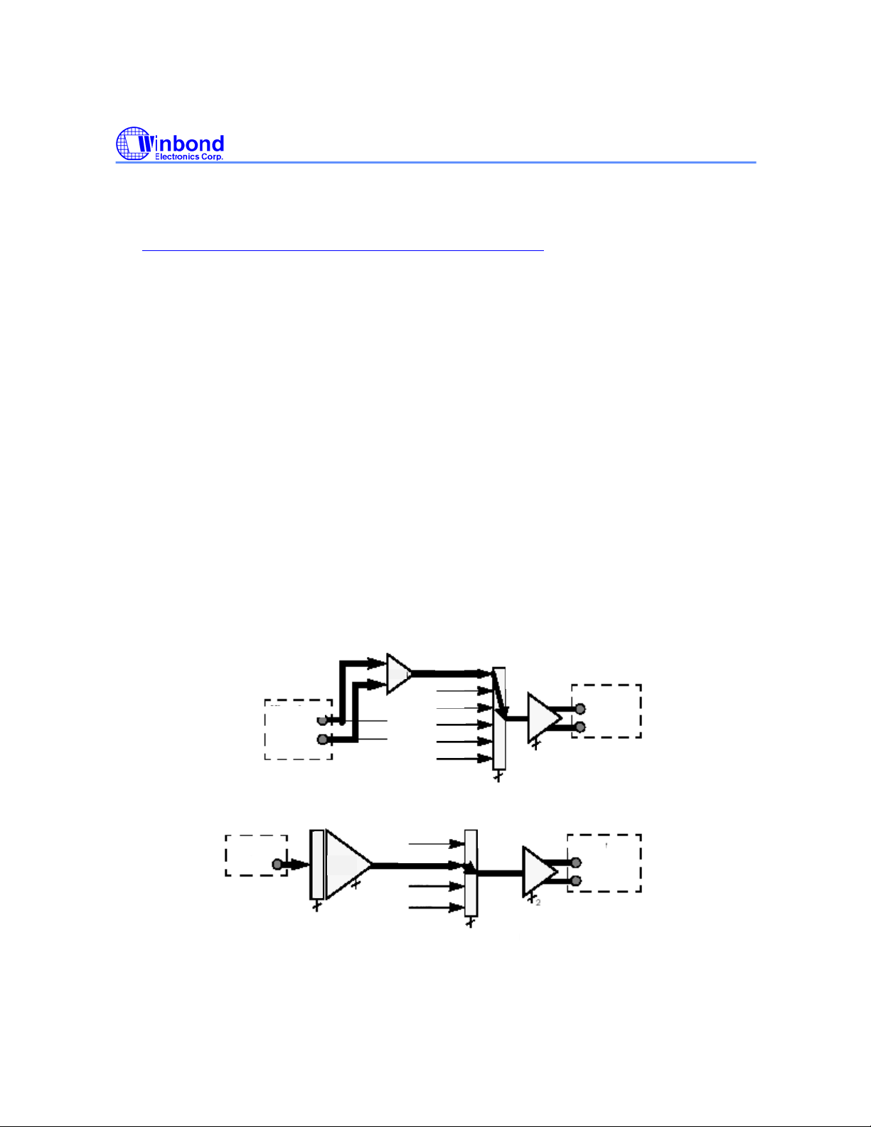
7.3.7. Feed Through Mode
The previous examples were dependent upon the device already being powered up and the various
paths being set through the device for the desired operation. To set up the device for the various
paths requires loading the two 16-bit Configuration Registers with the correct data. For example, in
the Feed Through Mode the device only needs to be powered up and a few paths selected.
This mode enables the ISD5100 Series to connect to a cellular or cordless base band phone chip set
without affecting the audio source or destination. There are two paths involved, the transmit path and
the receive path. The transmit path connects the Winbond chip’s microphone source through to the
microphone input on the base band chip set. The receive path connects the base band chip set’s
speaker output through to the speaker driver on the Winbond chip. This allows the Winbond chip to
substitute for those functions and incidentally gain access to the audio to and from the base band chip
set.
To set up the environment described above, a series of commands need to be sent to the ISD5100Series. First, the chip needs to be powered up as described in this section. Then the Configuration
Registers must be filled with the specific data to connect the paths desired. In the case of the Feed
Through Mode, most of the chip can remain powered down. The following figure illustrates the
affected paths.
Microphone
Mic+
Mic-
6 dB
FTHRU
INP
OL
FILT
SUM1
SUM2
Chip Set
ANA IN
ANA IN
AMP
1 [APD]
2 [AIG1,AIG0]
VOL
ANA IN AM P
FILTO
SUM2
OUTPUT
MUX
2 [OPS1,OPS0]
The figure above shows the part of the ISD5100 Series block diagram that is used in Feed Through
Mode. The rest of the chip will be powered down to conserve power. The bold lines highlight the audio
paths. Note that the Microphone to ANA OUT +/– path is differential.
on page 17.
NA OUT
MUX
3 [AOS2,AOS1,AOS0]
Chip Set
1 [AOPD]
eake
S
2 [OPA1,OPA0]
ANA OUT +
NA OUT-
SP+
SP-
- 22 -
Page 23

ISD5100 – SERIES
To select this mode, the following control bits must be configured in the ISD5100 Series configuration
registers. To set up the transmit path:
1. Select the FTHRU path through the ANA OUT MUX—Bits AOS0, AOS1 and AOS2 control the
state of the ANA OUT MUX. These are the D6, D7 and D8 bits respectively of Configuration
Register 0 (CFG0) and they should all be ZERO to select the FTHRU path.
2. Power up the ANA OUT amplifier—Bit AOPD controls the power up state of ANA OUT. This is
bit D5 of CFG0 and it should be a ZERO to power up the amplifier.
To set up the receive path:
1. Set up the ANA IN amplifier for the correct gain—Bits AIG0 and AIG1 control the gain settings
of this amplifier. These are bits D14 and D15 respectively of CFG0. The input level at this pin
determines the setting of this gain stage. The ANA IN Amplifier Gain Settings table
36 will help determine this setting. In this example, we will assume that the peak signal never
goes above 1 volt p-p single ended. That would enable us to use the 9 dB attenuation setting,
or where D14 is ONE and D15 is ZERO.
2. Power up the ANA IN amplifier—Bit AIPD controls the power up state of ANA IN. This is bit
D13 of CFG0 and should be a ZERO to power up the amplifier.
3. Select the ANA IN path through the OUTPUT MUX—Bits OPS0 and OPS1 control the state of
the OUTPUT MUX. These are bits D3 and D4 respectively of CFG0 and they should be set to
the state where D3 is ONE and D4 is ZERO to select the ANA IN path.
on page
4. Power up the Speaker Amplifier—Bits OPA0 and OPA1 control the state of the Speaker and
AUX amplifiers. These are bits D1 and D2 respectively of CFG0. They should be set to the
state where D1 is ONE and D2 is ZERO. This powers up the Speaker Amplifier and
configures it for its higher gain setting for use with a piezo speaker element and also powers
down the AUX output stage.
The status of the rest of the functions in the ISD5100 Series chip must be defined before the configuration registers settings are updated:
1. Power down the Volume Control Element—Bit VLPD controls the power up state of the
Volume Control. This is bit D0 of CFG0 and it should be set to a ONE to power down this
stage.
2. Power down the AUX IN amplifier—Bit AXPD controls the power up state of the AUX IN input
amplifier. This is bit D10 of CFG0 and it should be set to a ONE to power down this stage.
3. Power down the SUM1 and SUM2 Mixer amplifiers—Bits S1M0 and S1M1 control the SUM1
mixer and bits S2M0 and S2M1 control the SUM2 mixer. These are bits D7 and D8 in CFG1
and bits D5 and D6 in CFG1 respectively. All 4 bits should be set to a ONE to power down
these two amplifiers.
4. Power down the FILTER stage—Bit FLPD controls the power up state of the FILTER stage in
the device. This is bit D1 in CFG1 and should be set to a ONE to power down the stage.
5. Power down the AGC amplifier—Bit AGPD controls the power up state of the AGC amplifier.
This is bit D0 in CFG1 and should be set to a ONE to power down this stage.
Publication Release Date: October, 2003
- 23 - Revision 0.2
Page 24

ISD5100 – SERIES
6. Don’t Care bits—The following stages are not used in Feed Through Mode. Their bits may be
set to either level. In this example, we will set all the following bits to a ZERO. (a). Bit INS0, bit
D9 of CFG0 controls the Input Source Mux. (b). Bits AXG0 and AXG1 are bits D11 and D12
respectively in CFG0. They control the AUX IN amplifier gain setting. (c). Bits FLD0 and FLD1
are bits D2 and D3 respectively in CFG1. They control the sample rate and filter band pass
setting. (d). Bit FLS0 is bit D4 in CFG1. It controls the FILTER MUX. (e). Bits S1S0 and S1S1
are bits D9 and D10 of CFG1. They control the SUM1 MUX. (f). Bits VOL0, VOL1 and VOL2
are bits D11, D12 and D13 of CFG1. They control the setting of the Volume Control. (g). Bits
VLS0 and VLS1 are bits D14 and D15 of CFG1. They control the Volume Control MUX.
The end result of the above set up is
CFG0=0100 0100 0000 1011 (hex 440B)
and
CFG1=0000 0001 1110 0011 (hex 01E3).
Since both registers are being loaded, CFG0 is loaded, followed by the loading of CFG1. These two
registers must be loaded in this order. The internal set up for both registers will take effect synchronously with the rising edge of SCL.
7.3.8. Call Record
The call record mode adds the ability to record an incoming phone call. In most applications, the
ISD5100 Series would first be set up for Feed Through Mode as described above. When the user
wishes to record the incoming call, the setup of the chip is modified to add that ability. For the purpose
of this explanation, we will use the 6.4 kHz sample rate during recording.
The block diagram of the ISD5100 Series shows that the Multilevel Storage array is always driven
from the SUM2 SUMMING amplifier. The path traces back from there through the LOW PASS Filter,
THE FILTER MUX, THE SUM1 SUMMING amplifier, the SUM1 MUX, then from the ANA in amplifier.
Feed Through Mode has already powered up the ANA IN amp so we only need to power up and
enable the path to the Multilevel Storage array from that point:
1. Select the ANA IN path through the SUM1 MUX—Bits S1S0 and S1S1 control the state of the
SUM1 MUX. These are bits D9 and D10 respectively of CFG1 and they should be set to the
state where both D9 and D10 are ZERO to select the ANA IN path.
2. Select the SUM1 MUX input (only) to the S1 SUMMING amplifier—Bits S1M0 and S1M1
control the state of the SUM1 SUMMING amplifier. These are bits D7 and D8 respectively of
CFG1 and they should be set to the state where D7 is ONE and D8 is ZERO to select the
SUM1 MUX (only) path.
3. Select the SUM1 SUMMING amplifier path through the FILTER MUX—Bit FLS0 controls the
state of the FILTER MUX. This is bit D4 of CFG1 and it must be set to ZERO to select the
SUM1 SUMMING amplifier path.
- 24 -
Page 25

ISD5100 – SERIES
4. Power up the LOW PASS FILTER—Bit FLPD controls the power up state of the LOW PASS
FILTER stage. This is bit D1 of CFG1 and it must be set to ZERO to power up the LOW PASS
FILTER STAGE.
5. Select the 6.4 kHz sample rate—Bits FLD0 and FLD1 select the Low Pass filter setting and
sample rate to be used during record and playback. These are bits D2 and D3 of CFG1. To
enable the 6.4 kHz sample rate, D2 must be set to ONE and D3 set to ZERO.
6. Select the LOW PASS FILTER input (only) to the S2 SUMMING amplifier—Bits S2M0 and
S2M1 control the state of the SUM2 SUMMING amplifier. These are bits D5 and D6
respectively of CFG1 and they should be set to the state where D5 is ZERO and D6 is ONE to
select the LOW PASS FILTER (only) path.
In this mode, the elements of the original PASS THROUGH mode do not change. The sections of the
chip not required to add the record path remain powered down. In fact, CFG0 does not change and
remains
CFG0=0100 0100 0000 1011 (hex 440B).
CFG1 changes to
CFG1=0000 0000 1100 0101 (hex 00C5).
Since CFG0 is not changed, it is only necessary to load CFG1. Note that if only CFG0 was changed, it
would be necessary to load both registers.
7.3.9. Memo Record
The Memo Record mode sets the chip up to record from the local microphone into the chip’s Multilevel
Storage Array. A connected cellular telephone or cordless phone chip set may remain powered down
and is not active in this mode. The path to be used is microphone input to AGC amplifier, then through
the INPUT SOURCE MUX to the SUM1 SUMMING amplifier. From there the path goes through the
FILTER MUX, the LOW PASS FILTER, the SUM2 SUMMING amplifier, then to the MULTILEVEL
STORAGE ARRAY. In this instance, we will select the 5.3 kHz sample rate. The rest of the chip may
be powered down.
1. Power up the AGC amplifier—Bit AGPD controls the power up state of the AGC amplifier. This
is bit D0 of CFG1 and must be set to ZERO to power up this stage.
2. Select the AGC amplifier through the INPUT SOURCE MUX—Bit INS0 controls the state of
the INPUT SOURCE MUX. This is bit D9 of CFG0 and must be set to a ZERO to select the
AGC amplifier.
3. Select the INPUT SOURCE MUX (only) to the S1 SUMMING amplifier—Bits S1M0 and S1M1
control the state of the SUM1 SUMMING amplifier. These are bits D7 and D8 respectively of
CFG1 and they should be set to the state where D7 is ZERO and D8 is ONE to select the
INPUT SOURCE MUX (only) path.
4. Select the SUM1 SUMMING amplifier path through the FILTER MUX—Bit FLS0 controls the
state of the FILTER MUX. This is bit D4 of CFG1 and it must be set to ZERO to select the
SUM1 SUMMING amplifier path.
Publication Release Date: October, 2003
- 25 - Revision 0.2
Page 26

ISD5100 – SERIES
5. Power up the LOW PASS FILTER—Bit FLPD controls the power up state of the LOW PASS
FILTER stage. This is bit D1 of CFG1 and it must be set to ZERO to power up the LOW PASS
FILTER STAGE.
6. Select the 5.3 kHz sample rate—Bits FLD0 and FLD1 select the Low Pass filter setting and
sample rate to be used during record and playback. These are bits D2 and D3 of CFG1. To
enable the 5.3 kHz sample rate, D2 must be set to ZERO and D3 set to ONE.
7. Select the LOW PASS FILTER input (only) to the S2 SUMMING amplifier—Bits S2M0 and
S2M1 control the state of the SUM2 SUMMING amplifier. These are bits D5 and D6
respectively of CFG1 and they should be set to the state where D5 is ZERO and D6 is ONE to
select the LOW PASS FILTER (only) path.
To set up the chip for Memo Record, the configuration registers are set up as follows:
CFG0=0010 0100 0010 0001 (hex 2421).
CFG1=0000 0001 0100 1000 (hex 0148).
Only those portions necessary for this mode are powered up.
7.3.10. Memo and Call Playback
This mode sets the chip up for local playback of messages recorded earlier. The playback path is from
the MULTILEVEL STORAGE ARRAY to the FILTER MUX, then to the LOW PASS FILTER stage.
From there, the audio path goes through the SUM2 SUMMING amplifier to the VOLUME MUX,
through the VOLUME CONTROL then to the SPEAKER output stage. We will assume that we are
driving a piezo speaker element. This audio was previously recorded at 8 kHz. All unnecessary stages
will be powered down.
1. Select the MULTILEVEL STORAGE ARRAY path through the FILTER MUX—Bit FLS0, the
state of the FILTER MUX. This is bit D4 of CFG1 and must be set to ONE to select the
MULTILEVEL STORAGE ARRAY.
2. Power up the LOW PASS FILTER—Bit FLPD controls the power up state of the LOW PASS
FILTER stage. This is bit D1 of CFG1 and it must be set to ZERO to power up the LOW PASS
FILTER STAGE.
3. Select the 8.0 kHz sample rate—Bits FLD0 and FLD1 select the Low Pass filter setting and
sample rate to be used during record and playback. These are bits D2 and D3 of CFG1. To
enable the 8.0 kHz sample rate, D2 and D3 must be set to ZERO.
4. Select the LOW PASS FILTER input (only) to the S2 SUMMING amplifier —Bits S2M0 and
S2M1 control the state of the SUM2 SUMMING amplifier. These are bits D5 and D6
respectively of CFG1 and they should be set to the state where D5 is ZERO and D6 is ONE to
select the LOW PASS FILTER (only) path.
5. Select the SUM2 SUMMING amplifier path through the VOLUME MUX—Bits VLS0 and VLS1
control the state VOLUME MUX. These bits are bits D14 and D15, respectively of CFG1. They
should be set to the state where D14 is ONE and D15 is ZERO to select the SUM2 SUMMING
amplifier.
- 26 -
Page 27

ISD5100 – SERIES
6. Power up the VOLUME CONTROL LEVEL—Bit VLPD controls the power-up state of the
VOLUME CONTROL attenuator. This is Bit D0 of CFG0. This bit must be set to a ZERO to
power-up the VOLUME CONTROL.
7. Select a VOLUME CONTROL LEVEL—Bits VOL0, VOL1, and VOL2 control the state of the
VOLUME CONTROL LEVEL. These are bits D11, D12, and D13, respectively, of CFG1. A
binary count of 000 through 111 controls the amount of attenuation through that state. In most
cases, the software will select an attenuation level according to the desires of the current
users of the product. In this example, we will assume the user wants an attenuation of –12 dB.
For that setting, D11 should be set to ONE, D12 should be set to ONE, and D13 should be set
to a ZERO.
8. Select the VOLUME CONTROL path through the OUTPUT MUX—These are bits D3 and D4,
respectively, of CFG0. They should be set to the state where D3 is ZERO and D4 is a ZERO
to select the VOLUME CONTROL.
9. Power up the SPEAKER amplifier and select the HIGH GAIN mode—Bits OPA0 and OPA1
control the state of the speaker (SP+ and SP–) and AUX OUT outputs. These are bits D1 and
D2 of CFG0. They must be set to the state where D1 is ONE and D2 is ZERO to power-up the
speaker outputs in the HIGH GAIN mode and to power-down the AUX OUT.
To set up the chip for Memo or Call Playback, the configuration registers are set up as follows:
CFG0=0010 0100 0010 0010 (hex 2422).
CFG1=0101 1001 1101 0001 (hex 59D1).
Only those portions necessary for this mode are powered up.
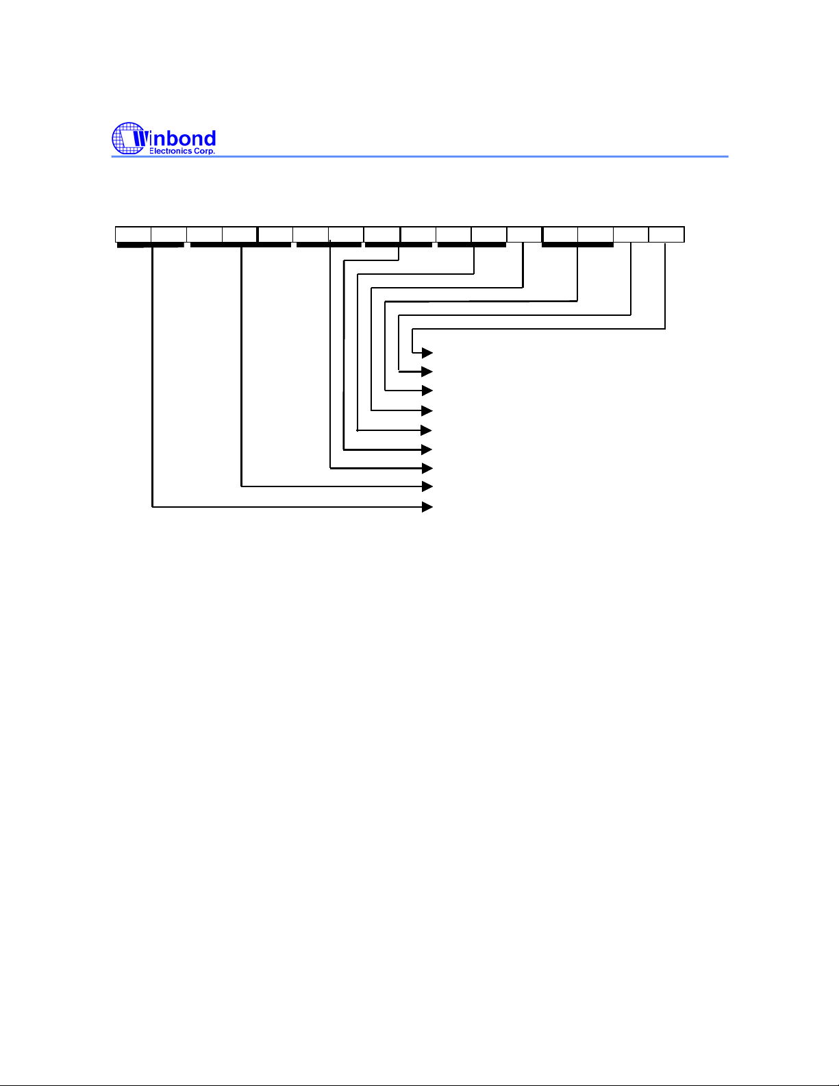
7.3.11. Message Cueing
Message cueing allows the user to skip through analog messages without knowing the actual physical
location of the message. This operation is used during playback. In this mode, the messages are
skipped 512 times faster than in normal playback mode. It will stop when an EOM marker is reached.
Then, the internal address counter will be pointing to the next message.
Publication Release Date: October, 2003
- 27 - Revision 0.2
Page 28

ISD5100 – SERIES
C=0
7.4. ANALOG MODE
7.4.1. Aux In and Ana In Description
The AUX IN is an additional audio input to the ISD5100-Series, such as from the microphone circuit in
a mobile phone “car kit.” This input has a nominal 694 mV p-p level at its minimum gain setting (0 dB).
See the AUX IN Amplifier Gain Settings table
(controlled by the I
The ANA IN pin is the analog input from the telephone chip set. It can be switched (by the serial bus)
to the speaker output, the array input or to various other paths. This pin is designed to accept a
nominal 1.11 Vp-p when at its minimum gain (6 dB) setting. See the ANA IN Amplifier Gain Settings
table on page 37. There is additional gain available in 3 dB steps controlled from the I2C interface, if
required, up to 15 dB.
AUX IN
Input
ANA IN
Input
2
C serial interface) up to 9 dB.
C
=0.1 µF
NOTE: f
.1 µF
NOTE: f
CUTOFF
CUTOFF
on page 37. Additional gain is available in 3 dB steps
Internal to the device
Rb
Ra
AUX IN
=
2πRaC
Input Amplifier
1
COUP
Internal to the device
Rb
Ra
ANA IN
=
2πRaC
Input Amplifier
1
COUP
- 28 -
Page 29

ISD5100 – SERIES
7.4.2. ISD5100 Series Analog Structure (left half) Description
IN PUT
SO UR CE
MU X
AGC AMP
AUX IN AMP
INSO Source
0 AGC AMP
1 AUX IN AMP
1 5 14 1 3 12 1 1 10 9 8 7 6 5 4 3 2 1 0
AIG1
AIG0 AIPD AXG1 AXG0 AXPD IN S0 AOS2 AOS1 AOS0 AOPD OPS1 OPS0 OPA1 OPA0 V LPD
1 5 14 1 3 12 1 1 10 9 8 7 6 5 4 3 2 1 0
VLS1 VL S0 V OL 2 VO L1 V OL 0 S1S1 S1 S0 S1M1 S1M0 S2 M1 S2M0 FLS0 FLD1 FLD0 FL PD AGPD
INP
(INS0)
FI LT O
AN A IN A MP
AR RA Y
SU M1
MU X
2 (S1S1,S1S0)
SUM1 SUMMING
AMP
Σ
2 (S1M1,S1M0)
S1M1 S1M0 SOURCE
0 0 BOTH
0 1 SUM1 MUX ONLY
1 0 INP Only
1 1 Power Down
S1S1 S1S0 SOURCE
0 0 ANA IN
0 1 ARRAY
1 0 FILTO
1 1 N/C
SU M 1
CFG0
CFG1
Publication Release Date: October, 2003
- 29 - Revision 0.2
Page 30

ISD5100 – SERIES
7.4.3. ISD5100 Series Aanalog Structure (right half) Description
FLS0 SOURCE
0 SUM1
1 ARRAY
FLPD CONDITION
0 Power Up
1 Power Down
FLD1 FLD0 SAMPLE
RATE
0 0 8 KHz 3.6 KHz
0 1 6.4 KHz 2.9 KHz
1 0 5.3 KHz 2.4 KHz
1 1 4.0 KHz 1.8 KHz
FILTER
FI LT E R
MU X
SUM1
ARRAY
ANA IN AMP
XCLK
FILTER
BANDWIDTH
1
(FLS0)1 (FLPD)
FILTO
LOW PASS
FILTER
IN TERN AL
CLOCK
FI LT O
2
(FLD1,FLD0)
ARRAY
SUM2 SUMMING
AMP
Σ
2 (S2 M 1,S2 M0 )
MUL TILEVEL
STO RA GE
ARRAY
15141312111098 76 54 32 10
VLS1
VLS0 VOL2 VOL1 VOL0 S1S1 S1S0 S1 M1 S1M0 S 2M1 S2M0 FLS0 FLD1 FLD0 FLPD AGPD
SU M2
S2M1 S2M0 SOURCE
0 0 BOTH
0 1 ANA IN ONLY
1 0 FILTO ONLY
1 1 Power Down
CFG1
- 30 -
Page 31

7.4.4. Volume Control Description
ISD5100 – SERIES
AN A IN A MP
SU M 2
SU M 1
IN P
VOL
MUX
2
(VLS1,VLS0)
VLS1 VLS0 SOURCE
0 0 ANA IN AMP
0 1 SUM2
1 0 SUM1
1 1 INP
VOL UME
CONTROL
3
( VOL 2,VOL1,V OL0 )
VOL2 VOL1 VOL0 ATTENUATION
0 0 0 0 dB
0 0 1 4 dB
0 1 0 8 dB
0 1 1 12 dB
1 0 0 16 dB
1 0 1 20 dB
1 1 0 24 dB
1 1 1 28 dB
1 (VL PD)
VO L
VLPD CONDITION
0 Power Up
1 Power Down
AIG1
AIG0 AIPD AXG1 AXG0 AXPD AOS2 AOS1 AOS0 AOPD OPS1 OPS0 OPA1 OPA0 VL PD
1514131211109876543210
VLS1
V LS0 VO L2 VOL 1 S1 S1 S1S0 S1M1 S1 M0 S2M1 S2M0 FLS0 FLD1 FLD0 FLPD AGPD
VOL0
INS0
CFG0
CFG1
Publication Release Date: October, 2003
- 31 - Revision 0.2
Page 32

ISD5100 – SERIES
7.4.5. Speaker and Aux Out Description
OUTPU T
MU X
VOL
ANA IN AMP
FILTO
SU M 2
2
(OPS1,OPS0)
OPS1 OPS0 SOURCE
0 0 VOL
0 1 ANA IN
1 0 FILTO
1 1 SUM2
2
(OPA1, OPA0)
OPA1 OPA0 SPKR DRIVE AUX OUT
AUX OUT
SP+
SP–
0 0 Power Down Power Down
0 1
1 0
1 1 Power Down
3.6 V
23.5 mWatt @ 8 Ω
1514131211109876543210
AIG1 AIG0 AIPD AXG1 AXG0 AXPD AOS2 AOS1 AOS0 AOPD OPS1 OPS0 OPA1 OPA0 VL PD
INS0
Car Kit
(1 Vp-p Ma x)
Sp eak e r
@ 150 Ω
P-P
CFG0
Power Down
Power Down
1 V
Max @ 5 KΩ
P-P
- 32 -
Page 33

ISD5100 – SERIES
7.4.6. Ana Out Description
*FTHR U
*IN P
*VOL
*FILT O
*SUM1
*SUM2
(AOPD)
(1 Vp-p max. from AUX IN or ARRAY)
( 69 4 mV p-p max . fro m mi cr opho ne i np ut )
AN A OU T +
AN A OU T –
1
Chi p Set
AOPD CONDITION
0 Power Up
1 Power Down
*DIFFERENTIAL PATH
3 (AOS2,AOS1,AOS0)
AOS2 AOS1 AOS0 SOURCE
0 0 0 FTHRU
0 0 1 INP
0 1 0 VOL
0 1 1 FILTO
1 0 0 SUM1
1 0 1 SUM2
1 1 0 N/C
1 1 1 N/C
1514131211109876 54 32 10
AI G1
AI G0 AIPD AXG1 AXG0 AXPD AOS2 AOS1 AOS0 AOPD OPS1 OPS0 OPA1 OPA0 V LPD
INS0
CFG0
7.4.7. Analog Inputs
Microphone Inputs
The microphone inputs transfer the voice signal to the on-chip AGC preamplifier or directly to the ANA
OUT MUX, depending on the selected path. The direct path to the ANA OUT MUX has a gain of 6
dB so a 208 mV p-p signal across the differential microphone inputs would give 416 mV p-p across
the ANA OUT pins. The AGC circuit has a range of 45 dB in order to deliver a nominal 694 mV p-p
into the storage array from a typical electric microphone output of 2 to 20 mV p-p. The input
impedance is typically 10k.
The ACAP pin provides the capacitor connection for setting the parameters of the microphone AGC
circuit. It should have a 4.7 µF capacitor connected to ground. It cannot be left floating. This is
because the capacitor is also used in the playback mode for the AutoMute circuit. This circuit reduces
the amount of noise present in the output during quiet pauses. Tying this pin to ground gives
maximum gain; to VCCA gives minimum gain for the AGC amplifier but will cancel the AutoMute
function.
Publication Release Date: October, 2003
- 33 - Revision 0.2
Page 34

MI C+
A
MIC–
6 dB
AGC
1 ( AG PD)
*
FTHRU
AGC
MIC IN
ISD5100 – SERIES
AGPD CONDITION
0 Power Up
1 Power Down
CAP
* Differential Path
1514131211109876543210
VLS1 VL S0 VOL2 VO L1 VOL0 S1S1 S1S0 S1M1 S1M0 S2M1 S2M0 FLS0 FLD1 FLD0 FLPD AG PD
To A utoM ute
(Playback Only)
CFG1
ANA IN (Analog Input)
The ANA IN pin is the analog input from the telephone chip set. It can be switched (by the I
interface) to the speaker output, the array input or to various other paths. This pin is designed to
accept a nominal 1.11 V p-p when at its minimum gain (6 dB) setting. There is additional gain
available, if required, in 3 dB steps, up to 15 dB. The gain settings are controlled from the I
interface.
ANA IN
Input
C
COUP =
0.1 µF
ANA IN
Input Amplifier
Gain
Setting
Resistor Ratio
(Rb/Ra)
Gain Gain2
00 63.9 / 102 0.625 -4.1
01 77.9 / 88.1 0.883 -1.1
10 92.3 / 73.8 1.250 1.9
11 106 / 60 1.767 4.9
Note: Ra & Rb are in kΩ
NOTE:
f
2xRaC
COUP
ANA IN Amplifier Gain Settings
(1)
0TLP Input
6 dB 1.110 0 0 0.625 0.694 2.22
9 dB 0.785 0 1 0.883 0.694 2.22
12 dB 0.555 1 0 1.250 0.694 2.22
(3)
V
P-P
CFG0 Setting
AIG1 AIG0
15 dB 0.393 1 1 1.767 0.694 2.22
(2)
Array
Gain
In/Out V
P-P
Speaker
Out V
(dB)
(4)
P-P
2
C
2
C
- 34 -
Page 35

ISD5100 – SERIES
1. Gain from ANA IN to SP+/-
2. Gain from ANA IN to ARRAY IN
3. 0TLP Input is the reference Transmission Level Point that is used for testing. This level is
typically 3 dB below clipping
4. Speaker Out gain set to 1.6 (High). (Differential)
AUX IN (Auxiliary Input)
The AUX IN is an additional audio input to the ISD5100-Series, such as from the microphone circuit in
a mobile phone “car kit.” This input has a nominal 694 mV p-p level at its minimum gain setting (0 dB).
See the following table. Additional gain is available in 3 dB steps (controlled by the I
9 dB.
AUX IN Input Modes
AUX IN
Input
C
COUP =
0.1 µF
NOTE:
f
CUTTOFF
2xRaC
ANA IN
Input Amplifier
COUP
Gain
Setting
00 40.1 / 40.1 1.0 0
01 47.0 / 33.2 1.414 3
10 53.5 / 26.7 2.0 6
11 59.2 / 21 2.82 9
Note: Ra & Rb are in kΩ
Resistor Ratio
(Rb/Ra)
AUX IN Amplifier Gain Settings
Setting
(1)
0TLP Input
(3)
V
P-P
CFG0
AXG1 AXG0
(2)
Array
Gain
In/Out V
0 dB 0.694 0 0 1.00 0.694 0.694
3 dB 0.491 0 1 1.41 0.694 0.694
6 dB 0.347 1 0 2.00 0.694 0.694
9 dB 0.245 1 1 2.82 0.694 0.694
1. Gain from AUX IN to ANA OUT
2. Gain from AUX IN to ARRAY IN
3. 0TLP Input is the reference Transmission Level Point that is used for testing. This level is typically
3 dB below clipping
4. Differential
2
C interface) up to
Gain Gain
(dB)
P-P
Out V
Speaker
P-P
(4)
(2)
Publication Release Date: October, 2003
- 35 - Revision 0.2
Page 36

ISD5100 – SERIES
7.5. DIGITAL MODE
7.5.1. Erasing Digital Data
The Digital Erase command can only erase an entire page at a time. This means that the D1
command only needs to include the 11-bit page address; the 5-bit for block address are left at 00000.
Once a page has been erased, each block may be written separately, 64 bits at a time. But, if a block
has been previously written then the entire page of 2048 bits must be erased in order to re-write (or
change) a block.
A sequence might be look like:
- read the entire page
- store it in RAM
- change the desired bit(s)
- erase the page
- write the new data from RAM to the entire page
7.5.2. Writing Digital Data
The Digital Write function allows the user to select a portion of the array to be used as digital memory.
The partition between analog and digital memory is left up to the user. A page can only be either
Digital or Analog, but not both. The minimum addressable block of memory in the digital mode is one
block or 64 bits, when reading or writing. The address sent to the device is the 11-bit row (or page)
address with the 5-bit scan (or block) address. However, one must send a Digital Erase before
attempting to change digital data on a page. This means that even when changing only one of the 32
blocks, all 32 blocks will need to be rewritten to the page. Command Sequence: The chip enters
digital mode by sending the ENTER DIGITAL MODE command from power down. Send the
DIGITAL WRITE @ ADDR command with the row address. After the address is entered, the data is
sent in one-byte packets followed by an I
is sent MSB first. The data transfer is ended when the master generates an I
only a partial block of data is sent before the STOP condition, “zero” is written in the remaining bytes;
that is, they are left at the erase level. An erased page (row) will be read as all zeros. The device can
buffer up to two blocks of data. If the device is unable to accept more data due to the internal write
process, the SCL line will be held LOW indicating to the master to halt data transfer. If the device
encounters an overflow condition, it will respond by generating an interrupt condition and an I
Acknowledge signal after the last valid byte of data. Once data transfer is terminated, the device
needs up to two cycles (64 us) to complete its internal write cycle before another command is sent. If
an active command is sent before the internal cycle is finished, the part will hold SCL LOW until the
current command is finished. After writing is complete, send the EXIT DIGITAL MODE command.
2
C acknowledge generated by the chip. Data for each block
2
C STOP condition. If
2
C Not
- 36 -
Page 37

ISD5100 – SERIES
7.5.3. Reading Digital Data
2
The Digital Read command utilizes the combined I
the chip using the write data direction. Then the data direction is reversed by sending a repeated
start condition, and the slave address with R/W set to 1. After this, the slave device (ISD5100Series) begins to send data to the master until the master generates a NACK. If the part encounters
an overflow condition, the
possible due to the master generating ACK signals.
Digital Write and Digital Read can be done a “block” at a time. Thus, only 64 bits need be read in
each Digital Read command sequence.
7.5.4. Example Command Sequences
An explanation and graphical representation of the Erase, Write and Read operations are found
below.
Note: All sequences assumes that the chip is in power-down mode before the commands are sent.
7.5.4.1. Erase Digital Data
Erase
=====
I2CStart
SendByte(0x80) - Write, Slave address zero
WaitACK
WaitSCLHigh
SendByte(0xc0) - Enter Digital Mode Command
WaitACK
WaitSCLHigh
I2CStop
I2CStart
SendByte(0x80) - Write, Slave address zero
WaitACK
WaitSCLHigh
SendByte(0xd1) - Digital Erase Command
WaitACK
WaitSCLHigh
SendByte(row/256) - high address byte
INT pin is pulled LOW. No other communication with the master is
C command format. That is, a command is sent to
Publication Release Date: October, 2003
- 37 - Revision 0.2
Page 38

WaitACK
WaitSCLHigh
SendByte(row%256) - low address byte
WaitACK
WaitSCLHigh
I2CStop
repeat until the number of RAC pulses are one less
than the number of rows to delete
{
wait RAC low
WAIT RAC high
}
Note: If only one row is going to be erased,
send the following STOP command immediately after
ERASE command and skip the loop above
I2CStart
SendByte(0x80) - Write, Slave address zero
WaitACK
WaitSCLHigh
SendByte(0xc0) - Stop digital erase
WaitACK
WaitSCLHigh
I2CStop
wait until erase of the last row has completed
{
wait RAC low
WAIT RAC high
}
I2CStart
SendByte(0x80) - Write, Slave address zero
WaitACK
ISD5100 – SERIES
- 38 -
Page 39

ISD5100 – SERIES
WaitSCLHigh
SendByte(0x40) - Exit Digital Mode Command
WaitACK
WaitSCLHigh
I2Cstop
Notes
1. Erase operations must be addressed on a Row boundary. The 5 LSB bits of the Low Address
Byte will be ignored.
2
2. I
C bus is released while erase proceeds. Other devices may use the bus until it is time to
execute the STOP command that causes the end of the Erase operation.
3. Host processor must count RAC cycles to determine where the chip is in the erase process,
one row per RAC cycle. RAC pulses LOW for 0.25 millisecond at the end of each erased
row. The erase of the "next" row begins with the rising edge of RAC. See the Digital Erase
RAC timing diagram on page 51.
4. When the erase of the last desired row begins, the following STOP command (Command Byte
= 80 hex) must be issued. This command must be completely given, including receiving the
ACK from the Slave before the RAC pin goes HIGH at the end of the row.
Publication Release Date: October, 2003
- 39 - Revision 0.2
Page 40

A
A
S
A
A
A
A
S
S
SS
80
ote
SLAVE ADDRESS
"N" RAC cycles
S SLAVE ADDRESSAW CON
A
W
Command Byte
Last erased row
N
D1
Note
DATA
High Addr. Byte Low Addr. Byte
LAVE ADDRE
ISD5100 – SERIES
P
Erase starts on falling
edge of Slave
acknowledge
DATA
P
Note 2
W
Command Byte
P
A
S SLAVE ADDRESSAW 40h
- 40 -
P
Page 41

SUGGESTED FLOW FOR DIGITAL ERASE IN
ISD5100-Series
ISD5100 – SERIES
80,C0
80,D1,nn,nn
COMMANDS
80 = PowerUp or Stop
C0 = Enter Digital Mode
D1 = Erase Digital Page@
40 = Exit Digital Mode
80,C0
ENTER DIGITAL
MODE
SEND ERASE
COMMAND
SEND STOP
COMMAND
BEFORE RAC
TO ERASE
MULTIPLE (n) PAGES
(ROWS)
NO
COUNT RAC
FOR n-1
YES
SEND STOP
COMMAND
BEFORE NEXT
RAC
RAC\ ~ 250 uS
80,C0
6/20/2002 BOJ
Revision B
80,40
WAIT FOR
RAC
YES
EXIT DIGITAL
MODE
DEVICE
POWERS DOWN
AUTOMATICALLY
NO
WAIT FOR
RAC
YES
STOP COMMAND MUST BE FINISHED BEFORE RAC\ RISES
RAC\ SIGNAL
250 uS
1.25 ms
NO
RAC\ ~ 125 uSRAC\ ~ 125 uS
125 uS
Publication Release Date: October, 2003
- 41 - Revision 0.2
Page 42

7.5.4.2. Write Digital Data
Write
=====
I2CStart
SendByte(0x80) - Write, Slave address zero
WaitACK
WaitSCLHigh
SendByte(0xc0) - Enter Digital Mode Command
WaitACK
WaitSCLHigh
I2CStop
I2CStart
SendByte(0x80) - Write, Slave address zero
WaitACK
WaitSCLHigh
SendByte(0xc9) - Write Digital Data Command
WaitACK
WaitSCLHigh
SendByte(row/256) - high address byte
WaitACK
WaitSCLHigh
SendByte(row%256) - low address byte
WaitACK
WaitSCLHigh
repeat until all data is sent
{
SendByte(data) - send data byte
WaitACK()
WaitSCLHigh()
}
I2CStop
ISD5100 – SERIES
- 42 -
Page 43

I2CStart
A
A
AHig
A
A
~
A
A
SendByte(0x80) - Write, Slave address zero
WaitACK
WaitSCLHigh
SendByte(0x40) - Exit Digital Mode Command
WaitACK
WaitSCLHigh
I2CStop
S SLAVE ADDRESS AW
S SLAVE ADDRESSAW CON
C9h
Command Byte
DATA
DATA
h Addr. Byte
DATA
ISD5100 – SERIES
P
DATA
Low Addr. Byte
~
~
DATA A P
~
S SLAVE ADDRESSAW 40h
Publication Release Date: October, 2003
- 43 - Revision 0.2
P
Page 44

ISD5100 – SERIES
SUGGESTED FLOW FOR DIGITAL WRITE IN ISD5100-Series
COMM ANDS
80 = PowerUp or Stop
C0 = Enter D igital Mod e
C9 = W rite Digital Page@
40 = Exit Digital Mode
80,C0
80,C9,nn,nn
ENTER DIGITAL
MODE
SE N D W RITE
COMMAND W/
START ADDRESS
SEND
DATA
BYTE
(SEND
NEXT
BYTE)
W A IT fo r S CL
HIGH
NO
6/24/2002 BOJ
Revision N/C
80,40
BYTE
COUNTER
=256?
YES
EX IT D IG ITAL
MODE
DEVICE
POWERS DOWN
AUTOMATICALLY
- 44 -
Page 45

7.5.4.3. Read Digital Data
Read
=====
I2CStart
SendByte(0x80) - Write, Slave address zero
WaitACK
WaitSCLHigh
SendByte(0xc0) - Enter Digital Mode
WaitACK
WaitSCLHigh
I2CStop
I2CStart
SendByte(0x80) - Write, Slave address zero
WaitACK
WaitSCLHigh
SendByte(0xe1) - Read Digital Data Command
WaitACK
WaitSCLHigh
SendByte(row/256) - high address byte
WaitACK
WaitSCLHigh()
SendByte(row%256) - low address byte
WaitACK
WaitSCLHigh
I2CStart - Send repeat start command
SendByte(0x81) - Read, Slave address zero
repeat until all data is read
{
data = ReadByte() - send clocks to read data byte
SendACK - send NACK on the last byte
WaitSCLHigh - The only flow control available
ISD5100 – SERIES
Publication Release Date: October, 2003
- 45 - Revision 0.2
Page 46

}
A
A
A
AHig
A
A
A
A
~
A
I2CStop()
I2CStart
SendByte(0x80) - Write, Slave address zero
WaitACK
WaitSCLHigh
SendByte(0x40) - Exit Digital Mode
WaitACK
WaitSCLHigh
I2CStop
S SLAVE ADDRESS
S SLAVE ADDRESSAW CON
W
Command Byte
E1h
DATA
h Addr. Byte
ISD5100 – SERIES
P
DATA
Low Addr. Byte
~ ~ ~
S SLAVE ADDRESS
R
S SLAVE ADDRESSAW 40h
DATA
- 46 -
DATA
PDATA N
P
Page 47

ISD5100 – SERIES
SUGGESTED FLOW FOR DIGITAL READ IN ISD5100-Series
COMMANDS
80 = PowerUp or Stop
C0 = Ente r D igital M ode
E1 = Read Digital Page@
40 = Exit Digital Mode
80,C0
80,E1,nn,nn
ENTER DIGITAL
MODE
SEND READ
COMMAND W /
START ADDRESS
READ
DATA
BYTE
(RE A D
NEXT
BYTE)
W A IT for S C L
HIGH
NO
BYTE
COUNTER
=256?
YES
EXIT DIGITAL
MODE
DEVICE
POW ERS DOW N
AUTOMATICALLY
6/24/2002 BOJ
Revision N/C
80,40
Publication Release Date: October, 2003
- 47 - Revision 0.2
Page 48

ISD5100 – SERIES
7.6. PIN DETAILS
7.6.1. Digital I/O Pins
SCL (Serial Clock Line)
The Serial Clock Line is a bi-directional clock line. It is an open-drain line requiring a pull-up resistor
to Vcc. It is driven by the "master" chips in a system and controls the timing of the data exchanged
over the Serial Data Line.
SDA (Serial Data Line)
2
The Serial Data Line carries the data between devices on the I
this line when the SCL is HIGH. State changes can only take place when the SCL is LOW. This is
a bi-directional line requiring a pull-up resistor to Vcc.
RAC (Row Address Clock)
RAC is an open drain output pin that normally marks the end of a row. At the 8 kHz sample frequency,
the duration of this period is 256 ms. There are 2048 pages of memory in the ISD5116 devices, 1024
pages in the ISD5108, and 572 pages in the ISD5104. RAC stays HIGH for 248 ms and stays LOW
for the remaining 8 ms before it reaches the end of the page.
C interface. Data must be valid on
1 ROW
RAC Waveform
During 8 KHz Operation
256 msec
T
RAC
8 msec
T
RACL
The RAC pin remains HIGH for 500 µsec and stays LOW for 15.6 µsec under the Message Cueing
mode. See the Timing Parameters table
rates. When a record command is first initiated, the RAC pin remains HIGH for an extra T
on page 64 for RAC timing information at other sample
period,
RACML
to load sample and hold circuits internal to the device. The RAC pin can be used for message
management techniques.
1 ROW
RAC Waveform
During Message Cueing
@ 8KHz Operation
500 usec
T
RACM
15.6 us
T
RACML
- 48 -
Page 49

ISD5100 – SERIES
RAC Waveform During Digital Erase @ 8kHz Operation
1.25 ms
TRACE
.25 ms
T
RACEL
INT (Interrupt)
INT is an open drain output pin. The ISD5100 Series interrupt pin goes LOW and stays LOW when an
Overflow (OVF) or End of Message (EOM) marker is detected. Each operation that ends in an EOM or
OVF generates an interrupt, including the message cueing cycles. The interrupt is cleared by a READ
STATUS instruction that will give a status byte out the SDA line.
XCLK (External Clock Input)
The external clock input for the ISD5100 Series product has an internal pull-down device. Normally,
the ISD5100 Series are operated at one of four internal rates selected for its internal oscillator by the
Sample Rate Select bits. If greater precision is required, the device can be clocked through the XCLK
pin at 4.096 MHz as described in section 7.4.3
on page 32.
Because the anti-aliasing and smoothing filters track the Sample Rate Select bits, one must, for
optimum performance, maintain the external clock at 4.096 MHz AND set the Sample Rate
Configuration bits to one of the four values to properly set the filters to the correct cutoff frequency as
described in section 7.4.3
on page 32. The duty cycle on the input clock is not critical, as the clock is
immediately divided by two internally. If the XCLK is not used, this input should be connected to V
External Clock Input Table
.
SSD
ISD5116
Duration
(Minutes)
ISD5108
Duration
(Minutes)
ISD5104
Duration
(Minutes)
ISD5102
Duration
(Minutes)
Sample
Rate
(kHz)
Required
Clock
(kHz)
FLD1 FLD0 Filter
Knee
(kHz)
8.73 4.36 2.18 1.08 8.0 4096 0 0 3.4
10.9 5.45 2.72 1.35 6.4 4096 0 1 2.7
13.1 6.55 3.27 1.63 5.3 4096 1 0 2.3
17.5 8.75 4.37 2.18 4.0 4096 1 1 1.7
Publication Release Date: October, 2003
- 49 - Revision 0.2
Page 50

ISD5100 – SERIES
A0, A1 (Address Pins)
These two pins are normally strapped for the desired address that the ISD5100 Series will have on the
2
C serial interface. If there are four of these devices on the bus, then each must be strapped
I
differently in order to allow the Master device to address them individually. The possible addresses
range from 80h to 87h, depending upon whether the device is being written to, or read from, by the
host. The ISD5100 Series have a 7-bit slave address of which only A0 and A1 are pin
programmable. The eighth bit (LSB) is the R/W bit. Thus, the address will be 1000 0xy0 or 1000
0xy1. (See the table in section 7.3.1
7.6.2. Analog I/O Pins
MIC+, MIC- (Microphone Input +/-)
The microphone input transfers the voice signal to the on-chip AGC preamplifier or directly to the ANA
OUT MUX, depending on the selected path. The direct path to the ANA OUT MUX has a gain of 6 dB
so a 208 mV p-p signal across the differential microphone inputs would give 416 mV p-p across the
ANA OUT pins. The AGC circuit has a range of 45 dB in order to deliver a nominal 694 mV p-p into
the storage array from a typical electret microphone output of 2 to 20 mV p-p. The input impedance is
typically 10k.
ANA OUT+, ANA OUT- (Analog Output +/-)
This differential output is designed to go to the microphone input of the telephone chip set. It is designed to drive a minimum of 5 k between the “+” and “–” pins to a nominal voltage level of 694 mV
p-p. Both pins have DC bias of approximately 1.2 VDC. The AC signal is superimposed upon this
analog ground voltage. These pins can be used single-ended, getting only half the voltage. Do NOT
ground the unused pin.
220 µF
Electret
Microphone
WM-54B
Panasonic
1.5kΩ
1.5kΩ
C
1.5kΩ
COUP
on page 13.)
MIC+
=0.1 µF Ra=10kΩ
10kΩ
MIC-
Internal to the device
FTHRU
MIC IN
NOTE: f
CUTOFF
=
2πRaC
1
COUP
- 50 -
Page 51

ISD5100 – SERIES
ACAP (AGC Capacitor)
This pin provides the capacitor connection for setting the parameters of the microphone AGC circuit. It
should have a 4.7 µF capacitor connected to ground. It cannot be left floating. This is because the
capacitor is also used in the playback mode for the AutoMute circuit. This circuit reduces the amount
of noise present in the output during quiet pauses. Tying this pin to ground gives maximum gain; tying
it to V
SP +, SP- (Speaker +/-)
This is the speaker differential output circuit. It is designed to drive an 8 speaker connected across
the speaker pins up to a maximum of 23.5 mW RMS power. This stage has two selectable gains, 1.32
and 1.6, which can be chosen through the configuration registers. These pins are biased to approximately 1.2 VDC and, if used single-ended, must be capacitively coupled to their load. Do NOT
ground the unused pin.
AUX OUT (Auxiliary Output)
The AUX OUT is an additional audio output pin to be used, for example, to drive the speaker circuit in
a “car kit.” It drives a minimum load of 5k and up to a maximum of 1V p-p. The AC signal is
superimposed on approximately 1.2 VDC bias and must be capacitively coupled to the load.
gives minimum gain for the AGC amplifier but cancels the AutoMute function.
CCA
OUT PUT
MUX
VO L
ANA IN AMP
FILTO
SUM2
2
OPS1 OPS0 SOURCE
0 0 VOL
0 1 ANA IN
1 0 FILTO
1 1 SUM2
15 14 13 12 11 10 9 8 7 6 5 4 3 2 1 0
AIG1 AIG0 AIP D AXG1 AXG0 AXP D AOS2 AOS1 AOS 0 AOPD OP S1 OPS0 OP A1 OPA0 VL PD
(OPS1,OPS0)
INS0
2
(OPA1, OPA0)
AUX OUT
SP+
SP–
OPS1 OPA0 SPKR DRIVE AUX OUT
0 0 Power Down Power Down
0 1 3.6 V
1 0 23.5 mWatt @ 8Ω Power Down
1 1 Power Down 1 V
Car K it
(1 Vp-p Max )
Speak er
CFG0
@150Ω Power Down
p.p
Max @ 5KΩ
p.p
Publication Release Date: October, 2003
- 51 - Revision 0.2
Page 52

ISD5100 – SERIES
ANA IN (Analog Input)
The ANA IN pin is the analog input from the telephone chip set. It can be switched (by the I
2
C
interface) to the speaker output, the array input or to various other paths. This pin is designed to
accept a nominal 1.11 V p-p when at its minimum gain (6 dB) setting. There is additional gain
available, if required, in 3 dB steps, up to 15 dB. The gain settings are controlled from the I
2
C
interface.
ANA IN Input Modes
(dB)
2
ANA IN
Input
C
COUP =
0.1 ìF
ANA IN
Input Amplifier
Gain
Setting
Resistor
Ration (Rb/Ra)
Gain Gain
00 63.9 / 102 0.625 -4.1
01 77.9 / 88.1 0.88 -1.1
10 92.3 / 73.8 1.25 1.9
11 106 / 60 1.77 4.9
Note: Ra & Rb are in kΩ
f
NOTE:
CUTTOFF
2xRaC
CCUP
ANA IN Amplifier Gain Settings
Setting
(1)
0TLP Input
(3)
V
P-P
CFG0
AIG1 AIG0
(2)
Array
Gain
In/Out V
P-P
Out V
Speaker
P-P
(4)
6 dB 1.110 0 0 0.625 0.694 2.22
9 dB 0.785 0 1 0.883 0.694 2.22
12 dB 0.555 1 0 1.250 0.694 2.22
15 dB 0.393 1 1 1.767 0.694 2.22
1. Gain from ANA IN to SP+/-
2. Gain from ANA IN to ARRAY IN
3. 0TLP Input is the reference Transmission Level Point that is used for testing. This level is typically 3
dB below clipping
4. Speaker Out gain set to 1.6 (High). (Differential)
- 52 -
Page 53

ISD5100 – SERIES
AUX IN (Auxiliary Input)
The AUX IN is an additional audio input to the ISD5100-Series, such as from the microphone circuit in
a mobile phone “car kit.” This input has a nominal 694 mV p-p level at its minimum gain setting (0 dB).
See the AUX IN Amplifier Gain Settings table
steps (controlled by the I
2
C interface) up to 9 dB.
AUX IN Input Modes
AUX IN
Input
C
COUP =
0.1 ìF
ANA IN
Input Amplifier
f
NOTE:
CUTTOFF
2xRaC
CCUP
on page 56. Additional gain is available in 3 dB
Gain
Setting
Resistor Ratio
(Rb/Ra)
Gain Gain
(2)
(dB)
00 40.1 / 40.1 1.0 0
01 47.0 / 33.2 1.414 3
10 53.5 / 26.7 2.0 6
11 59.2 / 21 2.82 9
Note: Ra & Rb are in kΩ
AUX IN Amplifier Gain Settings
Setting
(1)
0TLP Input
(3)
V
P-P
CFG0
AXG1 AXG0
(2)
Array
Gain
In/Out V
P-P
Out V
Speaker
P-P
(4)
0 dB 0.694 0 0 1.00 0.694 0.694
3 dB 0.491 0 1 1.41 0.694 0.694
6 dB 0.347 1 0 2.00 0.694 0.694
9 dB 0.245 1 1 2.82 0.694 0.694
1. Gain from AUX IN to ANA OUT
2. Gain from AUX IN to ARRAY IN
3. 0TLP Input is the reference Transmission Level Point that is used for testing. This level is typically 3 dB
below clipping
4. Differential
Publication Release Date: October, 2003
- 53 - Revision 0.2
Page 54

ISD5100 – SERIES
7.6.3. Power and Ground Pins
, V
V
CCA
To minimize noise, the analog and digital circuits in the ISD5100 Series devices use separate power
busses. These +3 V busses lead to separate pins. Tie the V
decouple both supplies as near to the package as possible.
V
SSA
The ISD5100 Series utilizes separate analog and digital ground busses. The analog ground (V
pins should be tied together as close to the package as possible and connected through a lowimpedance path to power supply ground. The digital ground (V
separate low impedance path to power supply ground. These ground paths should be large enough to
ensure that the impedance between the V
the die is connected to V
attach area must be connected to V
NC (Not Connect)
These pins should not be connected to the board at any time. Connection of these pins to any signal,
ground or V
(Voltage Inputs)
CCD
, V
(Ground Inputs)
SSD
may result in incorrect device behavior or cause damage to the device.
CC,
pins together as close as possible and
CCD
) pin should be connected through a
SSD
pins and the V
SSA
through the substrate resistance. In a chip-on-board design, the die
SSD
.
SSD
pin is less than 3. The backside of
SSD
SSA
)
- 54 -
Page 55

ISD5100 – SERIES
7.6.4. PCB Layout Examples
For SOIC package :
PC board traces and the three chip capacitors are on the bottom side of the board.
V
S
S
Note 3
D
(Digital Ground)
Note 1: V
SSD
separated back to the V
Note 1
traces should be kept
SS
point..
Note 2: V
separate back to the V
traces should be kept
CCD
CC
point.
Note 3: The Digital and Analog grounds
tie together at the power supply. The
V
CCA
and V
supplies will also need
CCD
filter capacitors per good engineering
practice (typ. 50 to 100 uF).
For TSOP package :
1
supply feed
Supply feed
V
SSA
1
O
O
O
O
O
O
O
O
O
O
O
O
O
O
Analog Ground
C1
C2
C3
Note 2
O
O
XCLK
O
O
V
C
C
D
O
V
SSA
O
O
C1=C2=C3=0.1 uF chip Capacitors
O
O
O
O
O
O
O
To
V
CCA
Note 3
[2]
V
V
Note
CCD
SSD
[3]
Note
Note
V
CCD
V
CCD
[1]
V
SSD
V
SSD
V
CCA
V
SSA
V
SSA
Notes:
[1]
V
traces should be kept separated back to the VSS supply feedpoint.
SSD
[2]
V
traces should be kept separate back to the VCC supply feedpoint.
CCD
[3]
Digital and Analog grounds tie together at power supply. The V
CCA
and V
supplies will also need filter
CCD
capacitors per good engineering practice (typ. 50 to 100 uF).
Publication Release Date: October, 2003
- 55 - Revision 0.2
V
CCA
V
SSA
Page 56

8.TIMING DIAGRAMS
r
8.1. I2C TIMING DIAGRAM
ISD5100 – SERIES
SDA
SCL
START
t
t
t
SU-STO
STOP
t
SU-DAT
t
f
t
LOW
t
SCLK
HIGH
t
f
- 56 -
Page 57
PARAMETER SYMBOL
SCL clock frequency
Hold time (repeated) START
condition. After this period, the first
clock pulse is generated
LOW period of the SCL clock
HIGH period of the SCL clock
Set-up time for a repeated START
condition
Data set-up time
Rise time of both SDA and SCL
signals
Fall time of both SDA and SCL
signals
Set-up time for STOP condition
Bus-free time between a STOP and
START condition
Capacitive load for each bus line
Noise margin at the LOW level for
each connected device (including
hysteresis)
Noise margin at the HIGH level for
each connected device (including
hysteresis)
2
C INTERFACE TIMING
I
STANDARD-MODE FAST-MODE
MIN. MAX. MIN. MAX.
f
SCL
t
HD-STA
t
LOW
t
HIGH
t
SU-STA
t
SU-DAT
tr
tf
t
SU-STO
t
BUF
Cb
VnL
VnH
0 100 0 400 kHz
4.0 - 0.6 - µs
4.7 - 1.3 - µs
4.0 - 0.6 - µs
4.7 - 0.6 - µs
250 - 100
- 1000 20 + 0.1C
- 300 20 + 0.1C
4.0 - 0.6 - µs
4.7 - 1.3 - µs
- 400 - 400 pF
0.1 VDD - 0.1 VDD - V
0.2 VDD - 0.2 VDD - V
ISD5100 – SERIES
UNIT
(1)
- ns
(2)
300 ns
b
(2)
300 ns
b
1. A Fast-mode I2C-interface device can be used in a Standard-mode I2C-interface system, but the
requirement t
> 250 ns must then be met. This will automatically be the case if the device does not
SU;DAT
stretch the LOW period of the SCL signal.
If such a device does stretch the LOW period of the SCL signal, it must output the next data bit to the SDA
line; t
r max
+ t
= 1000 + 250 = 1250 ns (according to the Standard-mode I2C -interface specification)
SU;DAT
before the SCL line is released.
= total capacitance of one bus line in pF. If mixed with HS mode devices, faster fall-times are
2. C
b
allowed.
Publication Release Date: October, 2003
- 57 - Revision 0.2
Page 58

8.2. PLAYBACK AND STOP CYCLE
ISD5100 – SERIES
SDA
SCL
ANA IN
ANA OUT
PLAY AT ADDR
DATA CLOCK PULSES
t
START
t
STOP
STOP
STOP
- 58 -
Page 59

8.3. EXAMPLE OF POWER UP COMMAND (FIRST 12 BITS)
ISD5100 – SERIES
Publication Release Date: October, 2003
- 59 - Revision 0.2
Page 60

ISD5100 – SERIES
9. ABSOLUTE MAXIMUM RATINGS
ABSOLUTE MAXIMUM RATINGS (PACKAGED PARTS)
Condition Value
Junction temperature 1500C
Storage temperature range -650C to +1500C
Voltage Applied to any pin (VSS - 0.3V) to (VCC + 0.3V)
Voltage applied to any pin (Input current limited to +/-20 mA) (VSS – 1.0V) to (VCC + 1.0V)
Lead temperature (soldering – 10 seconds) 3000C
VCC - VSS -0.3V to +5.5V
1.
Stresses above those listed may cause permanent damage to the device. Exposure to the absolute
maximum ratings may affect device reliability. Functional operation is not implied at these conditions.
ABSOLUTE MAXIMUM RATINGS (DIE)
(1)
(1)
Condition Value
Junction temperature 1500C
Storage temperature range -650C to +1500C
Voltage Applied to any pad (VSS - 0.3V) to (VCC + 0.3V)
VCC - VSS -0.3V to +5.5V
1.
Stresses above those listed may cause permanent damage to the device. Exposure to the absolute
maximum ratings may affect device reliability. Functional operation is not implied at these conditions.
- 60 -
Page 61

OPERATING CONDITIONS (PACKAGED PARTS)
Condition Value
Commercial operating temperature range
Extended operating temperature
Industrial operating temperature
Supply voltage (VCC)
Ground voltage (VSS)
1
. Case temperature
Die operating temperature range
Supply voltage (VCC)
Ground voltage (VSS)
1.
Case temperature
(2)
+2.7V to +3.3V
(3)
0V
2.
VCC = V
OPERATING CONDITIONS (DIE)
Condition Value
(2)
+2.7V to +3.3V
(3)
0V
2.
VCC = V
ISD5100 – SERIES
(1)
0
(1)
-200C to +700C
(1)
-400C to +850C
= V
= V
CCD
CCD
CCA
(1)
0
CCA
3.
VSS = V
3.
VSS = V
0
C to +700C
= V
SSA
0
C to +500C
= V
SSA
SSD
SSD
Publication Release Date: October, 2003
- 61 - Revision 0.2
Page 62

ISD5100 – SERIES
10. ELECTRICAL CHARACTERISTICS
10.1. GENERAL PARAMETERS
Symbol Parameters Min
(2)
Typ
VIL Input Low Voltage VCC x 0.2 V
VIH Input High Voltage VCC x 0.8 V
(1)
(2)
Max
Units Conditions
VOL SCL, SDA Output Low
0.4 V IOL = 3 µA
Voltage
V
Input low voltage for 2V
IL2V
interface
V
Input high voltage for 2V
IH2V
interface
V
RAC, INT Output Low Voltage 0.4 V IOL = 1 mA
OL1
VOH Output High Voltage V
ICC V
Current (Operating)
CC
- Playback
- Record
- Feedthrough
ISB V
Current (Standby) 1 10 µA (3)
CC
IIL Input Leakage Current
1.
Typical values: TA = 25°C and Vcc = 3.0 V.
2.
All min/max limits are guaranteed by Winbond via electrical testing or characterization. Not all
specifications are 100 percent tested.
3.
V
CCA
and V
summed together.
CCD
0.4 V Apply only to
SCL, SDA
1.6 V Apply only to
SCL, SDA
– 0.4 V IOL = -10 µA
CC
15
30
12
25
40
15
±1
mA
mA
mA
No Load
No Load
No Load
µA
(3)
(3)
(3)
- 62 -
Page 63

10.2. TIMING PARAMETERS
Symbol Parameters Min
(2)
Typ
FS Sampling Frequency 8.0
FCF Filter Knee
8.0 kHz (sample rate)
6.4 kHz (sample rate)
5.3 kHz (sample rate)
4.0 kHz (sample rate)
T
Record Duration
REC
8.0 kHz (sample rate)
6.4 kHz (sample rate)
5.3 kHz (sample rate)
4.0 kHz (sample rate)
ISD5116 ISD5108 ISD5104 ISD5102
8.73
10.9
13.1
17.5
4.36
5.45
6.55
8.75
(1)
Max
6.4
5.3
4.0
3.4
2.7
2.3
1.7
2.18
2.72
3.27
4.37
ISD5100 – SERIES
(2)
Units Conditions
1.08
1.35
1.63
2.18
kHz
kHz
kHz
kHz
kHz
kHz
kHz
kHz
min
min
min
min
(5)
(5)
(5)
(5)
Knee Point
Knee Point
Knee Point
Knee Point
(6)
(6)
(6)
(6)
(3)(7)
(3)(7)
(3)(7)
(3)(7)
T
Playback Duration
PLAY
8.0 kHz (sample rate)
6.4 kHz (sample rate)
5.3 kHz (sample rate)
4.0 kHz (sample rate)
T
Power-Up Delay
PUD
8.0 kHz (sample rate)
6.4 kHz (sample rate)
5.3 kHz (sample rate)
4.0 kHz (sample rate)
T
STOP
OR
PAUSE
Stop or Pause
Record or Play
8.0 kHz (sample rate)
6.4 kHz (sample rate)
5.3 kHz (sample rate)
4.0 kHz (sample rate)
T
RAC Clock Period
RAC
8.0 kHz (sample rate)
6.4 kHz (sample rate)
5.3 kHz (sample rate)
ISD5116 ISD5108 ISD5104 ISD5102
8.73
10.9
13.1
17.5
4.36
5.45
6.55
8.75
2.18
2.72
3.27
4.37
1
1
1
1
32
40
48
64
256
320
384
1.08
1.35
1.63
2.18
min
min
min
min
(6)
(6)
(6)
(6)
msec
msec
msec
msec
msec
msec
msec
msec
msec
msec
msec
(9)
(9)
(9)
Publication Release Date: October, 2003
- 63 - Revision 0.2
Page 64

4.0 kHz (sample rate) 512 msec (9)
T
RAC Clock Low Time
RACL
8.0 kHz (sample rate)
6.4 kHz (sample rate)
5.3 kHz (sample rate)
4.0 kHz (sample rate)
T
RAC Clock Period in
RACM
T
RACML
T
RACE
T
RACEL
THD Total Harmonic Distortion
Message Cueing Mode
8.0 kHz (sample rate)
6.4 kHz (sample rate)
5.3 kHz (sample rate)
4.0 kHz (sample rate)
RAC Clock Low Time in
Message Cueing Mode
8.0 kHz (sample rate)
6.4 kHz (sample rate)
5.3 kHz (sample rate)
4.0 kHz (sample rate)
RAC Clock Period in
Digital Erase Mode
8.0 kHz (sample rate)
6.4 kHz (sample rate)
5.3 kHz (sample rate)
4.0 kHz (sample rate)
RAC Clock Low Time in
Digital Erase mode
8.0 kHz (sample rate)
6.4 kHz (sample rate)
5.3 kHz (sample rate)
4.0 kHz (sample rate)
ANA IN to ARRAY,
ARRAY to SPKR
ISD5100 – SERIES
8
10
12.1
16
500
625
750
1000
15.6
19.5
23.4
31.2
1.25
1.56
1.87
2.50
0.25
0.31
0.37
0.50
1
1
2
2
msec
msec
msec
msec
µsec
µsec
µsec
µsec
µsec
µsec
µsec
µsec
msec
msec
msec
msec
msec
msec
msec
msec
%
%
@1 kHz at
0TLP, sample
rate = 5.3 kHz
- 64 -
Page 65
ISD5100 – SERIES
10.3. ANALOG PARAMETERS
MICROPHONE INPUT
Symbol Parameters Min
V
MIC +/- Input Voltage 300 mV Peak-to-Peak
MIC+/-
V
MIC (0TLP)
A
MIC
MIC +/- input reference
Gain from MIC +/- input to
(14)
transmission level point
(0TLP)
ANA OUT
(2)
Typ
(1)(14)
Max
(2)
Units Conditions
208 mV Peak-to-Peak
5.5 6.0 6.5 dB 1 kHz at V
(0TLP)
(4)(8)
(4)(10)
(4)
MIC
A
MIC +/- Gain Tracking +/-0.1 dB 1 kHz, +3 to –40
MIC (GT)
dB 0TLP Input
R
Microphone input resistance 10
MIC
MIC- and MIC+
kΩ
pins
A
Microphone AGC Amplifier
AGC
Range
6 40 dB Over 3-300 mV
Range
ANA IN
Symbol
V
V
A
A
A
A
R
(14)
Parameters Min
ANA IN Input Voltage 1.6 V Peak-to-Peak (6 dB
ANA IN
(2)
Typ
(1)(14)
Max
(2)
Units Conditions
gain setting)
ANA IN (0TLP)
ANA IN (sp)
ANA IN (AUX OUT)
ANA IN (0TLP) Input
Gain from ANA IN to SP+/- +6 to +15 dB 4 Steps of 3 dB
Voltage
Gain from ANA IN to AUX
1.1 V Peak-to-Peak (6 dB
gain setting)
-4 to +5 dB 4 Steps of 3 dB
OUT
ANA IN (GA)
ANA IN (GT)
ANA IN Gain Accuracy -0.5 +0.5 dB (11)
ANA IN Gain Tracking +/-0.1 dB 1000 Hz, +3 to –45
dB 0TLP Input,
6 dB setting
ANA IN Input Resistance (6
ANA IN
dB to +15 dB)
10 to 100
Depending on ANA
kΩ
IN Gain
(10)
Publication Release Date: October, 2003
- 65 - Revision 0.2
Page 66

ISD5100 – SERIES
p
(14)
AUX IN
Symbol
V
AUX IN
V
AUX IN (0TLP)
A
AUX IN (ANA OUT)
Parameters Min
(2)
Typ
AUX IN Input Voltage 1.0 V Peak-to-Peak (0 dB
AUX IN (0TLP) Input
694.2 mV Peak-to-Peak (0 dB
Voltage
Gain from AUX IN to ANA
0 to +9 dB 4 Steps of 3 dB
OUT
(1)(14)
Max
(2)
Units Conditions
gain setting)
gain setting)
A
AUX IN (GA)
A
AUX IN (GT)
R
AUX IN
AUX IN Gain Accuracy -0.5 +0.5 dB (11)
AUX IN Gain Tracking +/-0.1 dB 1000 Hz, +3 to –45
AUX IN Input Resistance 10 to 100
kΩ
(14)
SPEAKER OUTPUTS
Symbol
V
SP+/- Output Voltage (High
SPHG
R
SP+/- Output Load Imp.
SPLG
R
SP+/- Output Load Imp.
SPHG
CSP SP+/- Output Load Cap. 100 pF
V
SP+/- Output Bias Voltage
SPAG
V
Speaker Output DC Offset +/-100 mV
SPDCO
ICN
ANA IN/(SP+/-)
CRT
(SP+/-)/ANA
OUT
PSRR Power Supply Rejection
Parameters Min
Gain Setting)
(Low Gain)
(High Gain)
(Analog Ground)
ANA IN to SP+/- Idle
Channel Noise
SP+/- to ANA OUT Cross
Talk
Ratio
(2)
Typ
3.6 V Peak-to-Peak,
8 Ω OPA1, OPA0 = 10
70 150
1.2 VDC
-65 dB Speaker Load =
-65 dB 1 kHz 0TLP input to
-55 dB Measured with a 1
(1)(14)
Max
(2)
Units Conditions
Ω
DC
dB 0TLP Input, 0
dB setting
Depending on AUX
IN Gain
differential load =
150Ω, OPA1,
OPA0 = 01
OPA1, OPA0 = 01
With ANA IN to
Speaker, ANA IN
AC coupled to V
(12)(13)
150Ω
SSA
ANA IN, with
MIC+/- and AUX IN
AC coupled to V
SS,
and measured at
ANA OUT feed
through mode
(12)
kHz, 100 mV p-p
sine wave in
ut at
- 66 -
Page 67

ISD5100 – SERIES
VCC and VCC pins
FR Frequency Response (300-
3400 Hz)
P
Power Output (Low Gain
OUTLG
Setting)
SINAD SINAD ANA IN to SP+/- 62.5 dB 0TLP ANA In input
(14)
ANA OUT
Symbol
SINAD SINAD, MIC IN to ANA OUT 62.5 dB
SINAD SINAD, AUX IN to ANA OUT
ICO
NIC/ANA OUT
ICN
AUX IN/ANA
OUT
PSRR
(ANA OUT)
V
ANA OUT+ and ANA OUT- 1.2 VDC Inputs AC coupled
BIAS
V
ANA OUT+ to ANA OUT- +/- 100 mV
OFFSET
RL Minimum Load Impedance 5
FR Frequency Response (300-
CRT
ANA OUT/(SP+/-)
Parameters Min
(0 to 9 dB)
Idle Channel Noise –
Microphone
Idle Channel Noise – AUX
IN (0 to 9 dB)
Power Supply Rejection
Ratio
3400 Hz)
ANA OUT to SP+/- Cross
Talk
+
0.5
dB With 0TLP input to
ANA IN, 6 dB
(12)
setting
Guaranteed by
design
23.5 mW
RMS
(2)
Type
(1)(14)
Max
(2)
Units Conditions
62.5 dB
-65 dB
-65 dB
Differential load at
8Ω
minimum gain,
150Ω load
Load = 5kΩ
Load = 5kΩ
Load = 5kΩ
Load = 5kΩ
(12)(13)
(12)(13)
(12)(13)
(12)(13)
(12)(13)
-40 dB Measured with a 1
kHz, 100 mV
sine wave to V
V
pins
CCD
to V
SSA
Inputs AC coupled
DC
to V
SSA
Differential Load
kΩ
+
0.5
dB 0TLP input to
MIC+/- in
feedthrough mode.
0TLP input to AUX
IN in feedthrough
(12)
mode
-65 dB 1 kHz 0TLP output
from ANA OUT,
with ANA IN AC
coupled to V
and measured at
(12)
SP+/-
P-P
CCA
SSA,
,
Publication Release Date: October, 2003
- 67 - Revision 0.2
Page 68

ISD5100 – SERIES
CRT
ANA OUT/AUX
OUT
ANA OUT to AUX OUT
Cross Talk
-65 dB 1 kHz 0TLP output
from ANA OUT,
with ANA IN AC
coupled to V
and measured at
AUX OUT
(14)
AUX OUT
Symbol
V
AUX OUT
RL Minimum Load Impedance 5
CL Maximum Load Capacitance 100 pF
V
AUX OUT 1.2 VDC
BIAS
SINAD SINAD – ANA IN to AUX
ICN
(AUX OUT)
CRT
AUX OUT/ANA
OUT
Parameters Min
AUX OUT – Maximum
Output Swing
OUT
Idle Channel Noise – ANA IN
to AUX OUT
AUX OUT to ANA OUT
Cross Talk
(2)
Typ
1.0 V
(1(14))
Max
(2)
Units Conditions
5kΩ Load
KΩ
62.5 dB 0TLP ANA IN input,
minimum gain, 5k
load
-65 dB
Load=5kΩ
-65 dB 1 kHz 0TLP input to
ANA IN, with MIC
+/- and AUX IN AC
coupled to V
measured at SP+/-,
load = 5kΩ.
Referenced to
nominal 0TLP @
output
(12)(13)
(12)
(12)(13)
SSA,
,
SSA
(14)
VOLUME CONTROL
Symbol
A
Output Gain -28 to 0 dB 8 steps of 4 dB,
OUT
Parameters Min
(2)
Typ
(1)(14)
Max
(2)
Units Conditions
referenced to
output
Tolerance for each step -1.0 +1.0 dB ANA IN 1.0 kHz
0TLP, 6 dB gain
setting measured
differentially at
SP+/-
- 68 -
Page 69

ISD5100 – SERIES
Conditions
1. Typical values: TA = 25°C and Vcc = 3.0V.
2. All min/max limits are guaranteed by Winbond via electrical testing or characterization. Not all
specifications are 100 percent tested.
3. Low-frequency cut off depends upon the value of external capacitors (see Pin Descriptions).
4. Differential input mode. Nominal differential input is 208 mV p-p. (0TLP)
5. Sampling frequency can vary as much as –6/+4 percent over the industrial temperature and voltage
ranges. For greater stability, an external clock can be utilized (see Pin Descriptions).
6. Playback and Record Duration can vary as much as –6/+4 percent over the industrial temperature
and voltage ranges. For greater stability, an external clock can be utilized (See Pin Descriptions).
7. Filter specification applies to the low pass filter.
8. For optimal signal quality, this maximum limit is recommended.
= T
9. When a record command is sent, T
10. The maximum signal level at any input is defined as 3.17 dB higher than the reference transmission
level point. (0TLP) This is the point where signal clipping may begin.
11. Measured at 0TLP point for each gain setting. See the ANA IN table
and 55 respectively.
12. 0TLP is the reference test level through inputs and outputs. See the ANA IN table
on pages 54 and 55 respectively.
13. Referenced to 0TLP input at 1 kHz, measured over 300 to 3,400 Hz bandwidth.
RAC
RAC
+ T
14. For die, only typical values are applicable.
on the first page addressed.
RACL
and AUX IN table on pages 54
and AUX IN table
10.4. CHARACTERISTICS OF THE I2C SERIAL INTERFACE
The I2C interface is for bi-directional, two-line communication between different ICs or modules. The
two lines are a serial data line (SDA) and a serial clock line (SCL). Both lines must be connected to a
positive supply via a pull-up resistor. Data transfer may be initiated only when the interface bus is not
busy.
Bit transfer
One data bit is transferred during each clock pulse. The data on the SDA line must remain stable
during the HIGH period of the clock pulse, as changes in the data line at this time will be interpreted
as a control signal.
Publication Release Date: October, 2003
- 69 - Revision 0.2
Page 70

ISD5100 – SERIES
C
data line
stable;
data valid
Bit transfer on the I
Start and stop conditions
Both data and clock lines remain HIGH when the interface bus is not busy. A HIGH-to-LOW transition
of the data line while the clock is HIGH is defined as the start condition (S). A LOW-to-HIGH transition
of the data line while the clock is HIGH is defined as the stop condition (P).
SDA
SCL
START condition STOP condition
System configuration
Definition of START and STOP conditions
A device generating a message is a ‘transmitter’; a device receiving a message is the ‘receiver’. Th
System Configuration
A device generating a message is a ‘transmitter’; a device receiving a message is the ‘receiver’. The
device that controls the message I sthe ‘master’ and the devices that are controlled by the master are
the ‘slaves’.
changed
of data
allowed
2
-Bus
SDA
SCL
- 70 -
Page 71

ISD5100 – SERIES
MICROCONTROLLER
SDA
SCL
GATE
ARRAY
Example of an I2C-bus configuration using two microcontrollers
Acknowledge
The number of data bytes transferred between the start and stop conditions from transmitter to
receiver is unlimited. Each byte of eight bits is followed by an acknowledge bit. The acknowledge bit is
a HIGH level signal put on the interface bus by the transmitter during which time the master generates
an extra acknowledge related clock pulse. A slave receiver which is addressed must generate an
acknowledge after the reception of each byte. In addition, a master receiver must generate an
acknowledge after the reception of each byte that has been clocked out of the slave transmitter.
The device that acknowledges must pull down the SDA line during the acknowledge clock pulse so
that the SDA line is stable LOW during the HIGH period of the acknowledge related clock pulse (setup and hold times must be taken into consideration). A master receiver must signal an end of data to
the transmitter by not generating an acknowledge on the last byte that has been clocked out of the
slave. In this event, the transmitter must leave the data line HIGH to enable the master to generate a
stop condition.
LCD
DRIVER
ISD 5116
STATIC
RAM OR
EEPROM
DATA OUTPUT
BY TRANSMITTER
DATA OUTPUT
BY RECEIVER
SCL FROM
MASTER
START
condition
Acknowledge on the I
- 71 - Revision 0.2
not acknowledge
acknowledge
2
C-bus
Publication Release Date: October, 2003
dock pulse for
acknowledgement
Page 72

ISD5100 – SERIES
10.5. I2C PROTOCOL
Since the I2C protocol allows multiple devices on the bus, each device must have an address. This
address is known as a “Slave Address”. A Slave Address consists of 7 bits, followed by a single bit
that indicates the direction of data flow. This single bit is 1 for a Write cycle, which indicates the data is
being sent from the current bus master to the device being addressed. This single bit is a 0 for a Read
cycle, which indicates that the data is being sent from the device being addressed to the current bus
master. For example, the valid Slave Addresses for the ISD5100 Series device, for both Write and
Read cycles, are shown in section 7.3.1
Before any data is transmitted on the I2C interface, the current bus master must address the slave it
wishes to transfer data to or from. The Slave Address is always sent out as the 1
Start Condition sequence. An example of a Master transmitting an address to a ISD5100 Series slave
is shown below. In this case, the Master is writing data to the slave and the R/W bit is “0”, i.e. a Write
cycle. All the bits transferred are from the Master to the Slave, except for the indicated Acknowledge
bits. The following example details the transfer explained in section 7.3.1
datasheet.
Master Transmits to Slave Receiver (Write) Mode
acknowledgement
from slave
on page 13 of this datasheet.
acknowledgement
from slave
acknowledgement
from slave
st
byte following the
-2-3 on pages 13-20 of this
acknowledgement
from slave
SWAAAAPSLAVE ADDRESS COMMAND BYTE High ADDR. BYTE Low ADDR. BYTE
Start Bit Stop Bit
R/W
A common procedure in the ISD5100 Series is the reading of the Status Bytes. The Read Status
condition in the ISD5100 Series is triggered when the Master addresses the chip with its proper Slave
Address, immediately followed by the R/W bit set to a “1” and without the Command Byte being sent.
This is an example of the Master sending to the Slave, immediately followed by the Slave sending
data back to the Master. The “N” not-acknowledge cycle from the Master ends the transfer of data
from the Slave. The following example details the transfer explained in section 7.3.1
on page 13 of this
datasheet.
- 72 -
Page 73
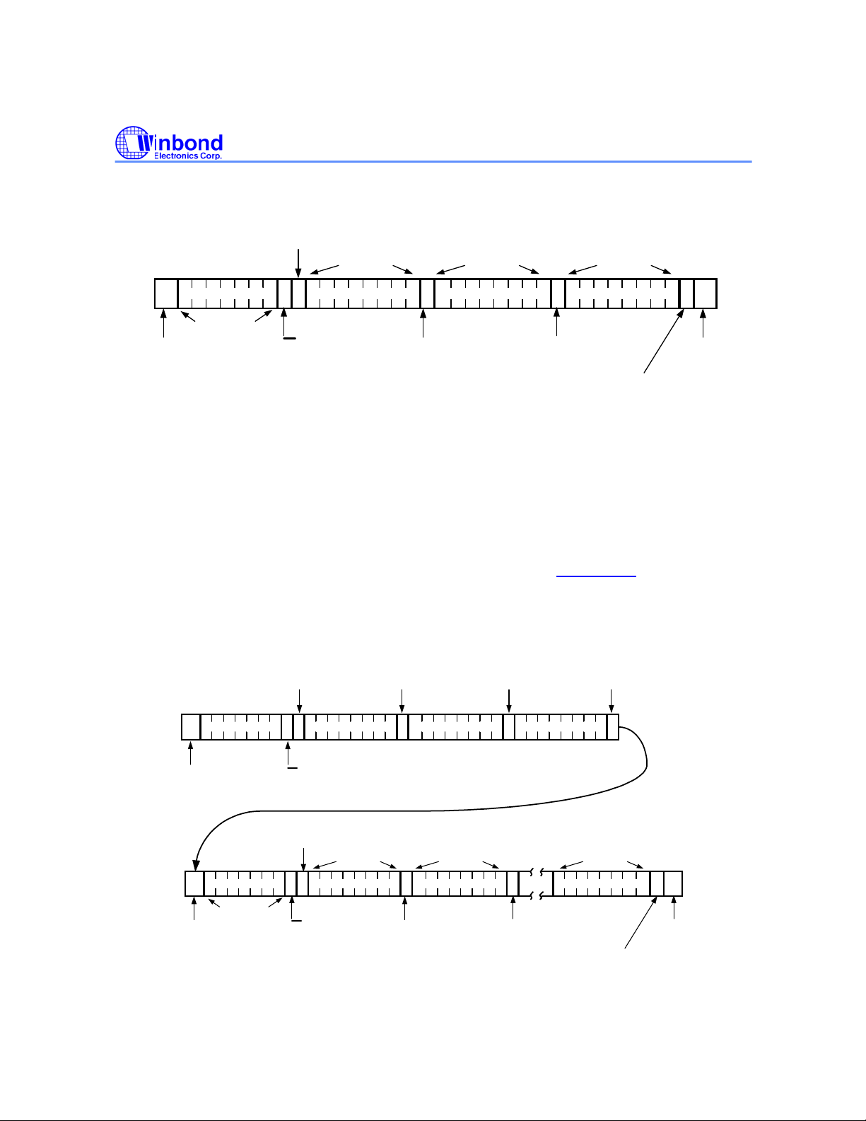
ISD5100 – SERIES
Master Reads from Slave immediately after first byte (Read Mode)
acknowledgement
from slave
From Slave From SlaveFrom Slave
SRA A A
From Master
Start Bit
From
Master
R/W
From
Master
acknowledgement
from Master
acknowledgement
from Master
not-acknowledged
from Master
N
Stop Bit
From
Master
PLow ADDR BYTESLAVE ADDRESS STATUS WORD High ADDR. BYTE
Another common operation in the ISD5100 Series is the reading of digital data from the chip’s memory
array at a specific address. This requires the I
ISD5100 Series Slave device, and then receive data from the Slave in a single I
2
C interface Master to first send an address to the
2
C operation. To
accomplish this, the data direction R/W bit must be changed in the middle of the command. The
following example shows the Master sending the Slave address, then sending a Command Byte and 2
bytes of address data to the ISD5100-Series, and then immediately changing the data direction and
reading some number of bytes from the chip’s digital array. An unlimited number of bytes can be read
in this operation. The “N” not-acknowledge cycle from the Master forces the end of the data transfer
from the Slave. The following example details the transfer explained in section 7.5.4
on page 47 of this
datasheet.
Master Reads from the Slave after setting data address in Slave (Write data address, READ Data)
acknowledgement
from slave
acknowledgement
from slave
acknowledgement
from slave
acknowledgement
from slave
SWA A A ASLAVE ADDRESS COMMAND BYTE High ADDR. BYTE Low ADDR. BYTE
Start Bit
From
Master
SRA A A
From Master
Start Bit
From
Master
R/W
From
Master
acknowledgement
from slave
R/W
From
Master
From Slave From SlaveFrom Slave
acknowledgement
from Master
acknowledgement
from Master
not-acknowled
from Master
N
Stop Bit
From
Master
P8 BITS of DATASLAVE ADDRESS 8 BITS of DATA 8 BITS of DATA
Publication Release Date: October, 2003
- 73 - Revision 0.2
Page 74

11. TYPICAL APPLICATION CIRCUIT
Recording via Microphone
ISD5100 – SERIES
To C
2
I
µ
C Interface &
Address Setting
V
CC
1.5K
1.5K
220
µ
F
Electret
microphone
1.5K
0.1 F
0.1 F
4.7 F
1
SCL
2
SDA
3
A1
4
A0
µ
8
MIC+
µ
10
MIC-
µ
13
ACAP
51XX
RAC
INT
V
CCD
V
CCD
V
CCA
V
SSD
V
SSD
V
SSA
V
SSA
V
SSA
SP+
SP-
24
25
27
28
17
15
23
16
14
V
CC
5
6
9
for message
management
0.1 F
0.1 F
µ
To C I/O
µ
(optional)
µ
SOIC / PDIP
Please see web site www.winbond-usa.com
- 74 -
for updates.
Page 75

ISD5100 – SERIES
1
12. PACKAGE SPECIFICATION
12.1. 28-LEAD 8X13.4MM PLASTIC THIN SMALL OUTLINE PACKAGE (TSOP) TYPE 1
28
28
27
27
26
26
25
25
24
24
23
23
22
22
21
21
20
20
19
19
18
18
17
17
16
16
15
15
G
F
C
E
2
2
3
3
4
5
6
7
8
9
10
11
12
13
14
4
5
6
7
8
9
10
11
12
13
14
A
B
D
H
J
I
Plastic Thin Small Outline Package (TSO P) Type 1 Dimensions
INCHES MILLIMETERS
Min Nom Max Min Nom Max
A
B 0.461 0.465 0.469 11.70 11.80 11.90
C
D 0.002 0.006 0.05 0.15
E 0.007 0.009 0.011 0.17 0.22 0.27
F
G 0.037 0.039 0.041 0.95 1.00 1.05
H
I
J 0.004 0.008 0.10 0.21
0.520 0.528 0.535 13.20 13.40 13.60
0.311 0.315 0.319 7.90 8.00 8.10
0.0217 0.55
0
0
0
3
0
6
0
0
0
3
0
6
0.020 0.022 0.028 0.50 0.55 0.70
Note:
Lead coplanarity to be within 0.004 inches.
Publication Release Date: October, 2003
- 75 - Revision 0.2
Page 76

ISD5100 – SERIES
12.2. 28-LEAD 300-MIL PLASTIC SMALL OUTLINE INTEGRATED CIRCUIT (SOIC)
27
26
2
25
24
45 67
3
232221 20 19 18 171615
9101112 13
8
14
A
G
C
28
1
B
D
E
Plastic Small Outline Integrated Circuit (SOIC) Dimensions
INCHES MILLIMETERS
F
H
Min Nom Max Min Nom Max
A
B
C
D
E
F
G
H
Lead coplanarity to be within 0.004 inches.
Note:
0.701 0.706 0.711 17.81 17.93 18.06
0.097 0.101 0.104 2.46 2.56 2.64
0.292 0.296 0.299 7.42 7.52 7.59
0.005 0.009 0.0115 0.127 0.22 0.29
0.014 0.016 0.019 0.35 0.41 0.48
0.050 1.27
0.400 0.406 0.410 10.16 10.31 10.41
0.024 0.032 0.040 0.61 0.81 1.02
- 76 -
Page 77

ISD5100 – SERIES
12.3. 28-LEAD 600-MIL PLASTIC DUAL INLINE PACKAGE (PDIP)
Plastic Dual Inline Package (PDIP) (P) Dimensions
Min Nom Max Min Nom Max
A 1.445 1.450 1.455 36.70 36.83 36.96
B1 0.150 3.81
B2 0.065 0.070 0.075 1.65 1.78 1.91
C1 0.600 0.625 15.24 15.88
C2 0.530 0.540 0.550 13.46 13.72 13.97
D 0.19 4.83
D1 0.015 0.38
E 0.125 0.135 3.18 3.43
F 0.015 0.018 0.022 0.38 0.46 0.56
G 0.055 0.060 0.065 1.40 1.52 1.65
H 0.100 2.54
J 0.008 0.010 0.012 0.20 0.25 0.30
S 0.070 0.075 0.080 1.78 1.91 2.03
0 0° 15° 0° 15°
INCHES
MILLIMETERS
Publication Release Date: October, 2003
- 77 - Revision 0.2
Page 78

12.4 ISD5116 DIE INFORMATION
ISD5100 – SERIES
ISD5116 Device
Die Dimensions
X: 4125 µm
Y: 8030 µm
Die Thickness
292.1 µm ± 12.7 µm
Pad Opening
Single pad: 90 x 90 µm
Double pad: 180 x 90 µm
[3]
V
SSD
V
SSD
≈
SDAA1SCL
A0
V
CCD
V
CCD
ISD5116
XCLK
INT
RAC
V
≈
SSA
V
SSA
MIC +
MIC -
ANA OUT +
ANA OUT -
ACAP
SP -
[2]
V
[2]
V
SSA
CCA
SP +
ANA IN
AUX OUT
AUX IN
Notes
1. The backside of die is internally connected to Vss. It MUST NOT be connected to any other potential or
damage may occur.
2. Double bond recommended, if treated as single doubled-pad.
3. This figure reflects the current die thickness. Please contact Winbond as this thickness may change in
the future.
- 78 -
Page 79

ISD5100 – SERIES
ISD5116 Pad Coordinates
(with respect to die center in µm)
Pad Pad Name X Axis Y Axis
V
Analog Ground 1879.45 3848.65
SSA
RAC Row Address Clock 1536.20 3848.65
INT
XCLK External Clock Input 475.60 3848.65
V
Digital Supply Voltage 288.60 3848.65
CCD
V
Digital Supply Voltage 73.20 3848.65
CCD
SCL Serial Clock Line -201.40 3848.65
A1 Address 1 -560.90 3848.65
SDA Serial Data Address -818.20 3848.65
A0 Address 0 -1369.40 3848.65
V
Digital Ground -1671.30 3848.65
SSD
V
Digital Ground -1842.90 3848.65
SSD
V
Analog Ground -1948.00 -3841.60
SSA
MIC+ Non-inverting Microphone Input -1742.20 -3841.60
MIC- Inverting Microphone Input -1509.70 -3841.60
ANA OUT+ Non-inverting Analog Output -1248.00 -3841.60
ANA OUT- Inverting Analog Output -913.80 -3841.60
ACAP AGC/AutoMute Cap -626.50 -3841.60
SP- Speaker Negative -130.70 -3841.60
V
Analog Ground 202.90 -3841.60
SSA
V
Analog Ground 292.90 -3841.60
SSA
SP+ Speaker Positive 626.50 -3841.60
V
Analog Supply Voltage 960.10 -3841.60
CCA
V
Analog Supply Voltage 1050.10 -3841.60
CCA
ANA IN Analog Input 1257.40 -3841.60
AUX IN Auxiliary Input 1523.00 -3841.60
AUX OUT Auxiliary Output 1767.20 -3841.60
Interrupt 787.40 3848.65
Publication Release Date: October, 2003
- 79 - Revision 0.2
Page 80

12.5 ISD5108 DIE INFORMATION
ISD5100 – SERIES
V
V
SSD
SDAA1SCL V
SSD
A0
INT
CCD
CCD
XCLK
V
RAC
V
SSA
ISD5108 Device
Die Dimensions (include scribe line)
X: 4230 µm
Y: 6090 µm
Die Thickness
292.1 µm ± 12.7 µm
Pad Opening
Single pad: 90 x 90 µm
Double pad: 180 x 90 µm
Notes
1. The backside of die is internally connected to Vss. It MUST NOT be connected to any other potential or
2. Double bond recommended, if treated as single doubled-pad.
3. This figure reflects the current die thickness. Please contact Winbond as this thickness may change in
[3]
damage may occur.
the future.
V
SSA
MIC +
≈
MIC -
ANA OUT +
ANA OUT -
ISD5108
SP -
ACAP
≈
[2]
V
[2]
V
SSA
CCA
SP +
ANA IN
AUX OUT
AUX IN
- 80 -
Page 81

ISD5100 – SERIES
ISD5108 Pad Coordinates
(with respect to die center in µm)
Pad Pad Name X Axis Y Axis
V
Analog Ground 1882.40 2820.65
SSA
RAC Row Address Clock 1539.15 2820.65
INT
XCLK External Clock Input 478.55 2820.65
V
Digital Supply Voltage 291.55 2820.65
CCD
V
Digital Supply Voltage 76.15 2820.65
CCD
SCL Serial Clock Line -198.45 2820.65
A1 Address 1 -557.95 2820.65
SDA Serial Data Address -815.25 2820.65
A0 Address 0 -1366.45 2820.65
V
Digital Ground -1668.35 2820.65
SSD
V
Digital Ground -1839.95 2820.65
SSD
V
Analog Ground -1945.05 -2821.60
SSA
MIC+ Non-inverting Microphone Input -1739.25 -2821.60
MIC- Inverting Microphone Input -1506.75 -2821.60
ANA OUT+ Non-inverting Analog Output -1245.05 -2821.60
ANA OUT- Inverting Analog Output -910.85 -2821.60
ACAP AGC/AutoMute Cap -623.55 -2821.60
SP- Speaker Negative -127.75 -2821.60
V
Analog Ground 205.85 -2821.60
SSA
V
Analog Ground 295.85 -2821.60
SSA
SP+ Speaker Positive 629.45 -2821.60
V
Analog Supply Voltage 963.05 -2821.60
CCA
V
Analog Supply Voltage 1053.05 -2821.60
CCA
ANA IN Analog Input 1260.35 -2821.60
AUX IN Auxiliary Input 1525.95 -2821.60
AUX OUT Auxiliary Output 1770.15 -2821.60
Interrupt 790.35 2820.65
Publication Release Date: October, 2003
- 81 - Revision 0.2
Page 82

12.6 ISD5104 DIE INFORMATION
ISD5100 – SERIES
V
V
SSD
SSD
SDAA1SCL
A0
V
CCD
V
CCD
XCLK
INT
RAC
V
SSA
ISD5104 Device
Die Dimensions (include scribe line)
X: 4230 µm
Y: 5046 µm
Die Thickness
292.1 µm ± 12.7 µm
Pad Opening
Single pad: 90 x 90 µm
Double pad: 180 x 90 µm
[3]
V
SSA
MIC +
≈
MIC -
ANA OUT +
ANA OUT -
Notes
1. The backside of die is internally connected to Vss. It MUST NOT be connected to any other potential or
damage may occur.
2. Double bond recommended, if treated as single doubled-pad.
3. This figure reflects the current die thickness. Please contact Winbond as this thickness may change in
the future.
ACAP
ISD5104
SP -
V
SSA
≈
[2]
V
SP +
CCA
[2]
ANA IN
AUX OUT
AUX IN
- 82 -
Page 83

ISD5100 – SERIES
ISD5104 Pad Coordinates
(with respect to die center in µm)
Pad Pad Name X Axis Y Axis
V
Analog Ground 1882.4 2306.65
SSA
RAC Row Address Clock 1539.15 2306.65
INT
XCLK External Clock Input 478.55 2306.65
V
Digital Supply Voltage 291.55 2306.65
CCD
V
Digital Supply Voltage 76.15 2306.65
CCD
SCL Serial Clock Line -198.45 2306.65
A1 Address 1 -557.95 2306.65
SDA Serial Data Address -815.25 2306.65
A0 Address 0 -1366.45 2306.65
V
Digital Ground -1839.95 2306.65
SSD
V
Digital Ground -1668.35 2306.65
SSD
V
Analog Ground -1945.05 -2311.60
SSA
MIC+ Non-inverting Microphone Input -1739.25 -2311.60
MIC- Inverting Microphone Input -1506.75 -2311.60
ANA OUT+ Non-inverting Analog Output -1245.05 -2311.60
ANA OUT- Inverting Analog Output -910.85 -2311.60
ACAP AGC/AutoMute Cap -623.55 -2311.60
SP- Speaker Negative -127.75 -2311.60
V
Analog Ground 205.85 -2311.60
SSA
V
Analog Ground 295.85 -2311.60
SSA
SP+ Speaker Positive 629.45 -2311.60
V
Analog Supply Voltage 963.05 -2311.60
CCA
V
Analog Supply Voltage 1053.05 -2311.60
CCA
ANA IN Analog Input 1260.35 -2311.60
AUX IN Auxiliary Input 1525.95 -2311.60
AUX OUT Auxiliary Output 1770.15 -2311.60
Interrupt 790.35 2306.65
Publication Release Date: October, 2003
- 83 - Revision 0.2
Page 84

12.7 ISD5102 DIE INFORMATION
ISD5100 – SERIES
SSD
SDAA1SCL
A0
V
V
SSD
V
CCD
CCD
XCLK
V
INT
RAC
V
SSA
ISD5102 Device
Die Dimensions (include scribe line)
X: 4230 µm
Y: 5046 µm
Die Thickness
292.1 µm ± 12.7 µm
Pad Opening
Single pad: 90 x 90 µm
Double pad: 180 x 90 µm
[3]
V
SSA
MIC +
≈
MIC -
ANA OUT +
ANA OUT -
Notes
1. The backside of die is internally connected to Vss. It MUST NOT be connected to any other potential or
damage may occur.
2. Double bond recommended, if treated as single doubled-pad.
3. This figure reflects the current die thickness. Please contact Winbond as this thickness may change in
the future.
ACAP
ISD5102
SP -
V
SSA
≈
[2]
V
SP +
CCA
[2]
ANA IN
AUX OUT
AUX IN
- 84 -
Page 85

ISD5100 – SERIES
ISD5102 Pad Coordinates
(with respect to die center in µm)
Pad Pad Name X Axis Y Axis
V
Analog Ground 1882.4 2306.65
SSA
RAC Row Address Clock 1539.15 2306.65
INT
XCLK External Clock Input 478.55 2306.65
V
Digital Supply Voltage 291.55 2306.65
CCD
V
Digital Supply Voltage 76.15 2306.65
CCD
SCL Serial Clock Line -198.45 2306.65
A1 Address 1 -557.95 2306.65
SDA Serial Data Address -815.25 2306.65
A0 Address 0 -1366.45 2306.65
V
Digital Ground -1839.95 2306.65
SSD
V
Digital Ground -1668.35 2306.65
SSD
V
Analog Ground -1945.05 -2311.60
SSA
MIC+ Non-inverting Microphone Input -1739.25 -2311.60
MIC- Inverting Microphone Input -1506.75 -2311.60
ANA OUT+ Non-inverting Analog Output -1245.05 -2311.60
ANA OUT- Inverting Analog Output -910.85 -2311.60
ACAP AGC/AutoMute Cap -623.55 -2311.60
SP- Speaker Negative -127.75 -2311.60
V
Analog Ground 205.85 -2311.60
SSA
V
Analog Ground 295.85 -2311.60
SSA
SP+ Speaker Positive 629.45 -2311.60
V
Analog Supply Voltage 963.05 -2311.60
CCA
V
Analog Supply Voltage 1053.05 -2311.60
CCA
ANA IN Analog Input 1260.35 -2311.60
AUX IN Auxiliary Input 1525.95 -2311.60
AUX OUT Auxiliary Output 1770.15 -2311.60
Interrupt 790.35 2306.65
Publication Release Date: October, 2003
- 85 - Revision 0.2
Page 86

ISD5100 – SERIES
13. ORDERING INFORMATION
Winbond Part Number Description
Product Family
ISD5100-Series
(1- to 16-minute durations)
Duration:
16 = ISD5116 (8 to 16 min)
08 = ISD5108 (4 to 8 min)
04 = ISD5104 (2 to 4 min)
02 = ISD5102 (1 to 2 min)
When ordering ISD5100 Series devices, please refer to the following valid part numbers.
I 5 1 -
}
}
Special Temperature Field:
Blank = Commercial Packaged (0°C to +70°C)
or Commercial Die (0°C to +50°C)
I = Industrial (–40°C to +85°C)
Package Type:
E = 28-Lead 8x13.4mm Plastic Thin Small Outline
Package (TSOP) Type 1
S = 28-Lead 300-Mil Plastic Small Outline Package (SOIC)
X = Die
P = 28-Lead 600-Mil Plastic Dual Inline Package (PDIP)
TSOP
SOIC
DIE
PDIP
I5116E I5108E I5104E I5102E
I5116EI I5108EI I5104EI I5102EI
I5116S I5108S I5104S I5102S
I5116SI I5108SI I5104SI I5102SI
I5116X I5108X I5104X I5102X
I5116P N/A N/A N/A
Part Number
For the latest product information, access Winbond’s worldwide website at
http://www.winbond-usa.com
- 86 -
Page 87

ISD5100 – SERIES
14. VERSION HISTORY
VERSION DATE DESCRIPTION
0.1 Mar 2003 New data sheet for the ISD5100-Series
0.2 Oct 2003 Add I5102 and I5104 products
Utilize TAD application in Functional Details
Reserve Load Address feature for factory uses
Simplify Playback mode
AnaIn: add kΩ for Ra & Rb
AuxIn: add kΩ for Ra & Rb, remove duplicate diagram, correct
parameter names in gain setting table & fix typos
Add application diagram
Add PCB layout example for TSOP package
2
I
C protocol: revise R/W bit =1 for reading status
Packaging: revise unit to mil instead of inch for SOIC & PDIP
Fix other typos
Publication Release Date: October, 2003
- 87 - Revision 0.2
Page 88

ISD5100 – SERIES
f
f
r
r
A
f
f
The contents of this document are provided only as a guide for the applications of Winbond products. Winbond
makes no representation or warranties with respect to the accuracy or completeness of the contents of this
publication and reserves the right to discontinue or make changes to specifications and product descriptions at
any time without notice. No license, whether express or implied, to any intellectual property or other right o
Winbond or others is granted by this publication. Except as set forth in Winbond's Standard Terms and
Conditions of Sale, Winbond assumes no liability whatsoever and disclaims any express or implied warranty o
merchantability, fitness for a particular purpose or infringement of any Intellectual property.
Winbond products are not designed, intended, authorized or warranted for use as components in systems o
equipments intended for surgical implantation, atomic energy control instruments, airplane or spaceship
instruments, transportation instruments, traffic signal instruments, combustion control instruments, or for othe
applications intended to support or sustain life. Further more, Winbond products are not intended for applications
wherein failure of Winbond products could result or lead to a situation wherein personal injury, death or severe
property or environmental injury could occur.
pplication examples and alternative uses of any integrated circuit contained in this publication are for illustration
only and Winbond makes no representation or warranty that such applications shall be suitable for the use
specified.
ISD® and ChipCorder® are treademarks of Winbond Electronics Corporation. SuperFlash® is the trademark o
Silicon Storage Technology, Inc.
The 100-year retention and 100K record cycle projections are based upon accelerated reliability tests, as
published in the Winbond Reliability Report, and are neither warranted nor guaranteed by Winbond.
Information contained in this ISD® ChipCorder® data sheet supersedes all data for the ISD ChipCorder products
published by ISD® prior to August, 1998.
This data sheet and any future addendum to this data sheet is(are) the complete and controlling ISD®
ChipCorder® product specifications. In the event any inconsistencies exist between the information in this and
other product documentation, or in the event that other product documentation contains information in addition to
the information in this, the information contained herein supersedes and governs such other information in its
entirety.
Copyright© 2003, Winbond Electronics Corporation. All rights reserved. ISD® is a registered trademark o
Winbond. ChipCorder® is a treademark of Winbond. All other trademarks are properties of their respective
owners.
Headquarters Winbond Electronics Corporation America Winbond Electronics (Shanghai) Ltd.
No. 4, Creation Rd. III 2727 North First Street, San Jose, 27F, 299 Yan An W. Rd. Shanghai,
Science-Based Industrial Park, CA 95134, U.S.A. 200336 China
Hsinchu, Taiwan TEL: 1-408-9436666 TEL: 86-21-62365999
TEL: 886-3-5770066 FAX: 1-408-5441798 FAX: 86-21-62356998
FAX: 886-3-5665577 http://www.winbond-usa.com/
http://www.winbond.com.tw/
Taipei Office Winbond Electronics Corporation Japan Winbond Electronics (H.K.) Ltd.
9F, No. 480, Pueiguang Rd. 7F Daini-ueno BLDG, 3-7-18 Unit 9-15, 22F, Millennium City,
Neihu District, Shinyokohama Kohoku-ku, No. 378 Kwun Tong Rd.,
Taipei, 114, Taiwan Yokohama, 222-0033 Kowloon, Hong Kong
TEL: 886-2-81777168 TEL: 81-45-4781881 TEL: 852-27513100
FAX: 886-2-87153579 FAX: 81-45-4781800 FAX: 852-27552064
Please note that all data and specifications are subject to change without notice.
All the trademarks of products and companies mentioned in this datasheet belong to their respective owners.
This product incorporates SuperFlash® technology licensed From SST.
- 88 -
 Loading...