

Page 1
Single-Chip Voice Record/Playback Devices
8-, 10-, 12-, and 16-Minute Durations
GENERAL DESCRIPTION
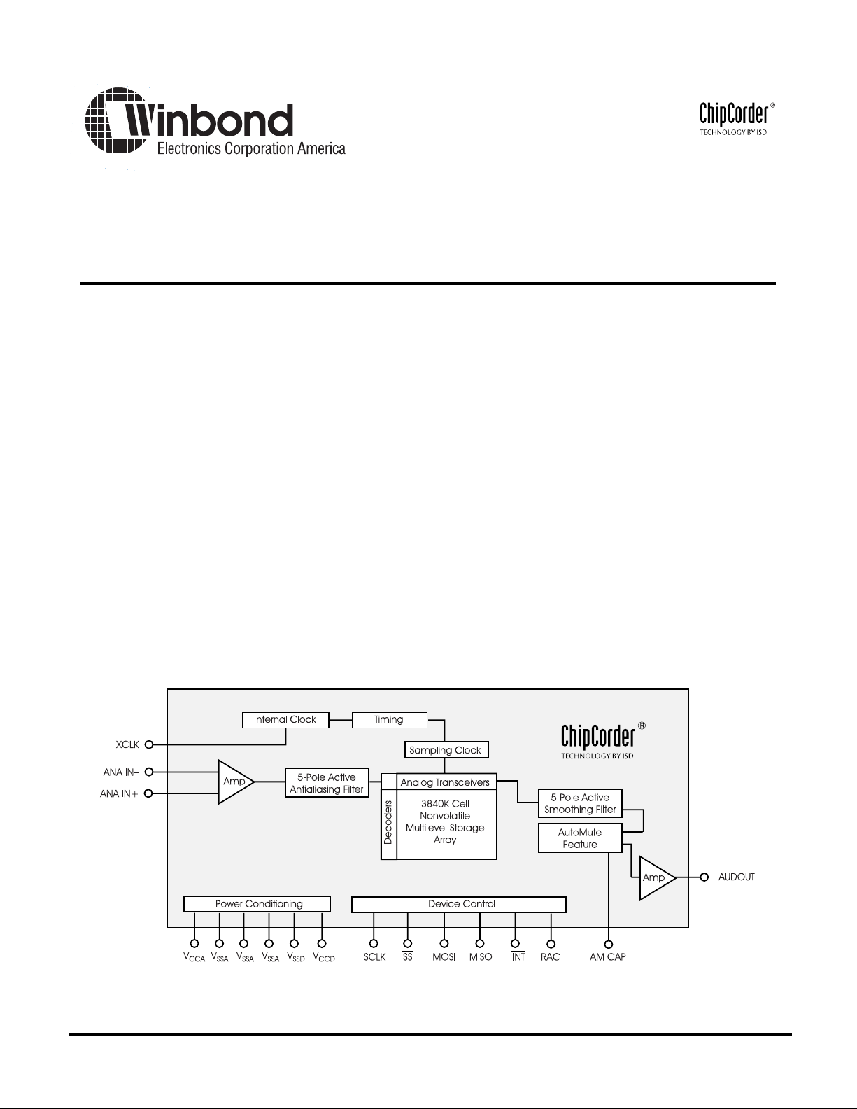
The ISD4004 ChipCorder
quality, 3-volt, single-chip record/playback solutions for 8- to 16-minute m essaging appli cations
which are ideal fo r cellular phone s an d other portable products. The CMOS-based devic es include
an on-chip oscillator, antialiasing filter, smoothing
filter, AutoMute™ feature, audio amplifier, and
high density, multilevel Flash storage array. The
ISD4004 series is designed to be used in a microprocessor- or microcontroller-based system. Address and control are accomplished through a
Serial Peripheral Interface (SPI) or Microwire Serial
Interface to minimize pin count.
®
Products provide high-
ISD4004 Series
Recordings are stored in on-chip nonvolatile
memory cells, providing zero-power message
storage. This unique, single-chip solution is made
possible through ISD’s patent ed multilevel storage
technology. Voice and audio signals are stored
directly into memory in their natural form, providing
high-qualit y, solid-state voic e reproduction.
Figure: ISD4004 Series Block Diagram
August 2000
ISD/Winbond · 2727 North First Street, San Jose, CA 95134 · TEL: 408/943-6666 · FAX: 408/544-1787 · http://www.isd.com
Page 2
ISD4004 Series
FEATURES
• Single-chip voice record/playback solution
• Single +3 volt supply
• Low-power consu m ption
– Operating current:
Play = 15 mA (typical)
I
CC
I
Rec = 25 mA (typical)
CC
– Standby current: 1 µA (typical)
• Single-chip duratio ns of 8, 10, 12, and
16 minutes
• High-quality, natural voice/au dio reproduction
• AutoMute feature pr o vid es background noise
attenuation during peri od s of sil ence
• No algorithm development required
• Microcontroller SPI or Microwire™ Serial
Interface
Table: ISD4004 Series Summary
• Fully addressable to han dle multiple
messages
• Nonvolatile message storage
• Power consumption controlled by SPI
or Microwire control register
• 100-year message retention (typical)
• 100K record cycles (typical)
• On-chip clock source
• Available in die form, PDIP, SOIC, and TSOP
• Extended temper atur e (–20° C to +7 0°C) and
industrial temperature (–40°C to +85°C)
versions available
Part
Number
ISD4004-08M 8.0 8.0 3.4
ISD4004-10M 10.0 6.4 2.7
ISD4004-12M 12.0 5.3 2.3
ISD4004-16M 16.0 4.0 1.7
Duration
(minutes)
Input Sample
Rate (KHz)
Typical Filter Pass
Band (KHz)
ii
Voice Solutions in Silicon
™
Page 3

Table of Contents
DETAILED DESCRIPTION . . . . . . . . . . . . . . . . . . . . . . . . . . . . . . . . . . . . . . . . . . . . . . . . . . . . . . . . . . . . . . . 1
Speech/Sound Quality . . . . . . . . . . . . . . . . . . . . . . . . . . . . . . . . . . . . . . . . . . . . . . . . . . . . . . . . . . . . 1
Duration . . . . . . . . . . . . . . . . . . . . . . . . . . . . . . . . . . . . . . . . . . . . . . . . . . . . . . . . . . . . . . . . . . . . . . . 1
Flash Storage . . . . . . . . . . . . . . . . . . . . . . . . . . . . . . . . . . . . . . . . . . . . . . . . . . . . . . . . . . . . . . . . . . . 1
Microcontroller Interface . . . . . . . . . . . . . . . . . . . . . . . . . . . . . . . . . . . . . . . . . . . . . . . . . . . . . . . . . .1
Programming . . . . . . . . . . . . . . . . . . . . . . . . . . . . . . . . . . . . . . . . . . . . . . . . . . . . . . . . . . . . . . . . . . . 1
PIN DESCRIPTIONS . . . . . . . . . . . . . . . . . . . . . . . . . . . . . . . . . . . . . . . . . . . . . . . . . . . . . . . . . . . . . . . . . . . 1
Voltage Inputs (V
Ground Inputs (V
Non-Inverting Analog Input (ANA IN+) . . . . . . . . . . . . . . . . . . . . . . . . . . . . . . . . . . . . . . . . . . . . . . . . 3
Inverting Analog Input (ANA IN–) . . . . . . . . . . . . . . . . . . . . . . . . . . . . . . . . . . . . . . . . . . . . . . . . . . . . 3
Audio Output (AUD OUT) . . . . . . . . . . . . . . . . . . . . . . . . . . . . . . . . . . . . . . . . . . . . . . . . . . . . . . . . . . 3
Slave Select (S S
Master Out Slave In (MOSI) . . . . . . . . . . . . . . . . . . . . . . . . . . . . . . . . . . . . . . . . . . . . . . . . . . . . . . . . . 3
Master In Slave Out (MISO) . . . . . . . . . . . . . . . . . . . . . . . . . . . . . . . . . . . . . . . . . . . . . . . . . . . . . . . . . 3
Serial Clock (SCLK) . . . . . . . . . . . . . . . . . . . . . . . . . . . . . . . . . . . . . . . . . . . . . . . . . . . . . . . . . . . . . . .3
Interrupt (INT
Row Address Clock (RAC) . . . . . . . . . . . . . . . . . . . . . . . . . . . . . . . . . . . . . . . . . . . . . . . . . . . . . . . . . 4
External Clock Input (XCLK) . . . . . . . . . . . . . . . . . . . . . . . . . . . . . . . . . . . . . . . . . . . . . . . . . . . . . . . . 4
AutoMute™ Feature (AM CAP) . . . . . . . . . . . . . . . . . . . . . . . . . . . . . . . . . . . . . . . . . . . . . . . . . . . . . .4
) . . . . . . . . . . . . . . . . . . . . . . . . . . . . . . . . . . . . . . . . . . . . . . . . . . . . . . . . . . . . . . . . . . . 3
, V
CCA
, V
SSA
) . . . . . . . . . . . . . . . . . . . . . . . . . . . . . . . . . . . . . . . . . . . . . . . . . . . . . . . . . . . . . . . . . 3
) . . . . . . . . . . . . . . . . . . . . . . . . . . . . . . . . . . . . . . . . . . . . . . . . . . . . . . . 1
CCD
) . . . . . . . . . . . . . . . . . . . . . . . . . . . . . . . . . . . . . . . . . . . . . . . . . . . . . . . . .1
SSD
SERIAL PERIPHERAL INTERFACE (SPI) DESCRIPTION . . . . . . . . . . . . . . . . . . . . . . . . . . . . . . . . . . . . . . . . . . . . 5
Message Cueing . . . . . . . . . . . . . . . . . . . . . . . . . . . . . . . . . . . . . . . . . . . . . . . . . . . . . . . . . . . . . . . . 5
Power-Up Sequence . . . . . . . . . . . . . . . . . . . . . . . . . . . . . . . . . . . . . . . . . . . . . . . . . . . . . . . . . . . . . 6
SPI Port . . . . . . . . . . . . . . . . . . . . . . . . . . . . . . . . . . . . . . . . . . . . . . . . . . . . . . . . . . . . . . . . . . . . . . . .7
SPI Control Register . . . . . . . . . . . . . . . . . . . . . . . . . . . . . . . . . . . . . . . . . . . . . . . . . . . . . . . . . . . . . . 7
TIMING DIAGRAMS . . . . . . . . . . . . . . . . . . . . . . . . . . . . . . . . . . . . . . . . . . . . . . . . . . . . . . . . . . . . . . . . . . 14
DEVICE PHYSICAL DIMENSIONS . . . . . . . . . . . . . . . . . . . . . . . . . . . . . . . . . . . . . . . . . . . . . . . . . . . . . . . . 18
ORDERING INFORMATION . . . . . . . . . . . . . . . . . . . . . . . . . . . . . . . . . . . . . . . . . . . . . . . . . . . . . . . . . . . . 23
ISD
iii
Page 4

ISD4004 Series
FIGURES, CHARTS, AND TABLES IN THE ISD4004 SERIES DATA SHEET
Figure 1: ISD4004 Series TSOP and PDIP/SOIC Pinouts . . . . . . . . . . . . . . . . . . . . . . . . . . . . . . . . 2
Figure 2: ISD4004 Series ANA IN Modes . . . . . . . . . . . . . . . . . . . . . . . . . . . . . . . . . . . . . . . . . . . 2
Figure 3: SPI Po rt . . . . . . . . . . . . . . . . . . . . . . . . . . . . . . . . . . . . . . . . . . . . . . . . . . . . . . . . . . . . . 7
Figure 4: SPI Inter face Simplif ied Bloc k Diagram . . . . . . . . . . . . . . . . . . . . . . . . . . . . . . . . . . . . 8
Figure 5: Timin g Diag ram . . . . . . . . . . . . . . . . . . . . . . . . . . . . . . . . . . . . . . . . . . . . . . . . . . . . . 14
Figure 6: 8-Bit Command Format . . . . . . . . . . . . . . . . . . . . . . . . . . . . . . . . . . . . . . . . . . . . . . 14
Figure 7: 24-Bit Command Format . . . . . . . . . . . . . . . . . . . . . . . . . . . . . . . . . . . . . . . . . . . . . 15
Figure 8: Pl ayback/Record and Stop Cycle . . . . . . . . . . . . . . . . . . . . . . . . . . . . . . . . . . . . . . . 15
Figure 9: Applicat ion Example Using SPI. . . . . . . . . . . . . . . . . . . . . . . . . . . . . . . . . . . . . . . . . . 16
Figure 10: Application Example Using Microwire . . . . . . . . . . . . . . . . . . . . . . . . . . . . . . . . . . . . 17
Figure 11: Application Example Using SPI Port on Microcontroller . . . . . . . . . . . . . . . . . . . . . . . 17
Figure 12: 28-Lead 8x13.4 mm Plastic Thin Small Outline Package (TSOP) Type I (E) . . . . . . . . 18
Figure 13: 28-Lead 0.600-Inch Plastic Dual Inline Package (PDIP) (P) . . . . . . . . . . . . . . . . . . . . 19
Figure 14: 28-Lead 0.300-Inch Plastic Small Outline Integrated Circuit (SOIC) (S) . . . . . . . . . . . 20
Figure 15: ISD4004 Series Bonding Physical Layout (Unpackaged Die) . . . . . . . . . . . . . . . . . . . 21
Table 1: External Clock Input Clocking Table . . . . . . . . . . . . . . . . . . . . . . . . . . . . . . . . . . . . . . 4
Table 2: Opcode Summary . . . . . . . . . . . . . . . . . . . . . . . . . . . . . . . . . . . . . . . . . . . . . . . . . . . 6
Table 3: SPI Control Register . . . . . . . . . . . . . . . . . . . . . . . . . . . . . . . . . . . . . . . . . . . . . . . . . . . 7
Table 4: Absolute Maximum Ratings (Packaged Parts) . . . . . . . . . . . . . . . . . . . . . . . . . . . . . . . 8
Table 5: Operating Conditions (Packaged Parts) . . . . . . . . . . . . . . . . . . . . . . . . . . . . . . . . . . . 8
Table 6: DC Parameters (Packaged Parts) . . . . . . . . . . . . . . . . . . . . . . . . . . . . . . . . . . . . . . . . 9
Table 7: AC Parameters (Packaged Parts) . . . . . . . . . . . . . . . . . . . . . . . . . . . . . . . . . . . . . . . . 9
Table 8: Absolute Maximum Ratings (Die) . . . . . . . . . . . . . . . . . . . . . . . . . . . . . . . . . . . . . . . . 11
Table 9: Operating Conditions (Die) . . . . . . . . . . . . . . . . . . . . . . . . . . . . . . . . . . . . . . . . . . . . 11
Table 10: DC Parameters (Die) . . . . . . . . . . . . . . . . . . . . . . . . . . . . . . . . . . . . . . . . . . . . . . . . . 11
Table 11: AC Parameters (Die) . . . . . . . . . . . . . . . . . . . . . . . . . . . . . . . . . . . . . . . . . . . . . . . . . 12
Table 12: SPI AC Parameters . . . . . . . . . . . . . . . . . . . . . . . . . . . . . . . . . . . . . . . . . . . . . . . . . . . 13
Table 13: Plastic Thin Small Outline Package (TSOP) Type I (E) Dimensions . . . . . . . . . . . . . . . . 18
Table 14: Plastic Dual Inline Package (PDIP) (P ) Dime nsions . . . . . . . . . . . . . . . . . . . . . . . . . . . 19
Table 15: Plastic Small Outline Integrated Circ uit (SOIC) (S) Dimensions . . . . . . . . . . . . . . . . . . 20
Table 16: ISD4004 Serie s Devic e Pin/Pad Designations, with Respect to Die Cent er (µm) . . . . 22
iv
Voice Solutions in Silicon™
Page 5

ISD4004 Series
DETAILED DESCRIPTION
SPEECH/SOUND QUALITY
The ISD4004 ChipCorder series includes devices
offered at 4.0, 5.3, 6.4, and 8.0 KHz sampling f requencies, allowin g the user a choice of speech
quality options. Increasing the duration within a
product series decreases the sampling frequency
and bandwidth, which affects sound quality.
Please refer to the ISD4004 Ser ies Pro duct Summary
table on the second page to compare filter pass
band and product durations.
The speech samples ar e stored directly into on-chip
nonvolatile memory without the digitization and
compression associated with other solutions. Direct analog stor age provides a natural sounding
reproduction of voice, music, tones, and sound
effects not available with most solid-state solutions.
DURATION
To meet end system requirements, the ISD4004 series products are single-chip solutions at 8, 10, 12,
16 minutes.
FLASH STORAGE
One of the benefits of ISD’s ChipCorder technology
is the use of on-chip nonvolatile memory, which provides zero-power message storage. The message
is retained for up to 100 years (typically) without
power. In addition, the device can be re-recorded (typically) over 100,000 times.
MICROCONTROLLER INTERFACE
A four-wire (SCLK, MOSI, MISO, SS) SPI interface is
provided for ISD4004 control and addressing
functions. The ISD4004 is configured to operate as
a peripheral slave device, with a microcontrollerbased SPI bus interface. Read/Write access to all
the internal reg isters occurs through this SPI interface. An interrupt signal (INT
only Status Register are provided for handshake
purposes.
) and internal read-
PROGRAMMING
The ISD4004 series is also ideal for playback-only
applications, where single or multiple message
Playback is controlled through the SPI port. Once
the desired message configuration is created, duplicates can easily be generated via an ISD programmer.
PIN DESCRIPTIONS
VOLTAGE INPUTS (V
To minimize noise, the analog and digital circuits
in the ISD4004 devices use separate power busses.
These +3 V busses are brought out to separate
pins and should be tied together as close to the
supply as possible. In addition, these supplies
should be decoupled as close to the package as
possible.
GROUND INPUTS (V
The ISD4004 series utilizes separate analog and
digital ground busses. The analog ground (V
pins should be tied together as close to the package as possible and connected through a lowimpedance path to power supply ground. The
digital ground (V
through a separate low -imp edance path t o pow er supply ground. Th ese ground paths should b e
large enough to en sure that the impedanc e between the V
3 W. The backside of the die is connected to V
through the substrate resistance. In a chip-onboard design, the die attach area must be connected to V
SSA
or left floating.
SS
, V
CCA
SSA
SSD
pins and the V
)
CCD
, V
)
SSD
) pin should be connected
pin is less than
SSD
SSA
SS
)
ISD
1
Page 6
ISD4004 Series
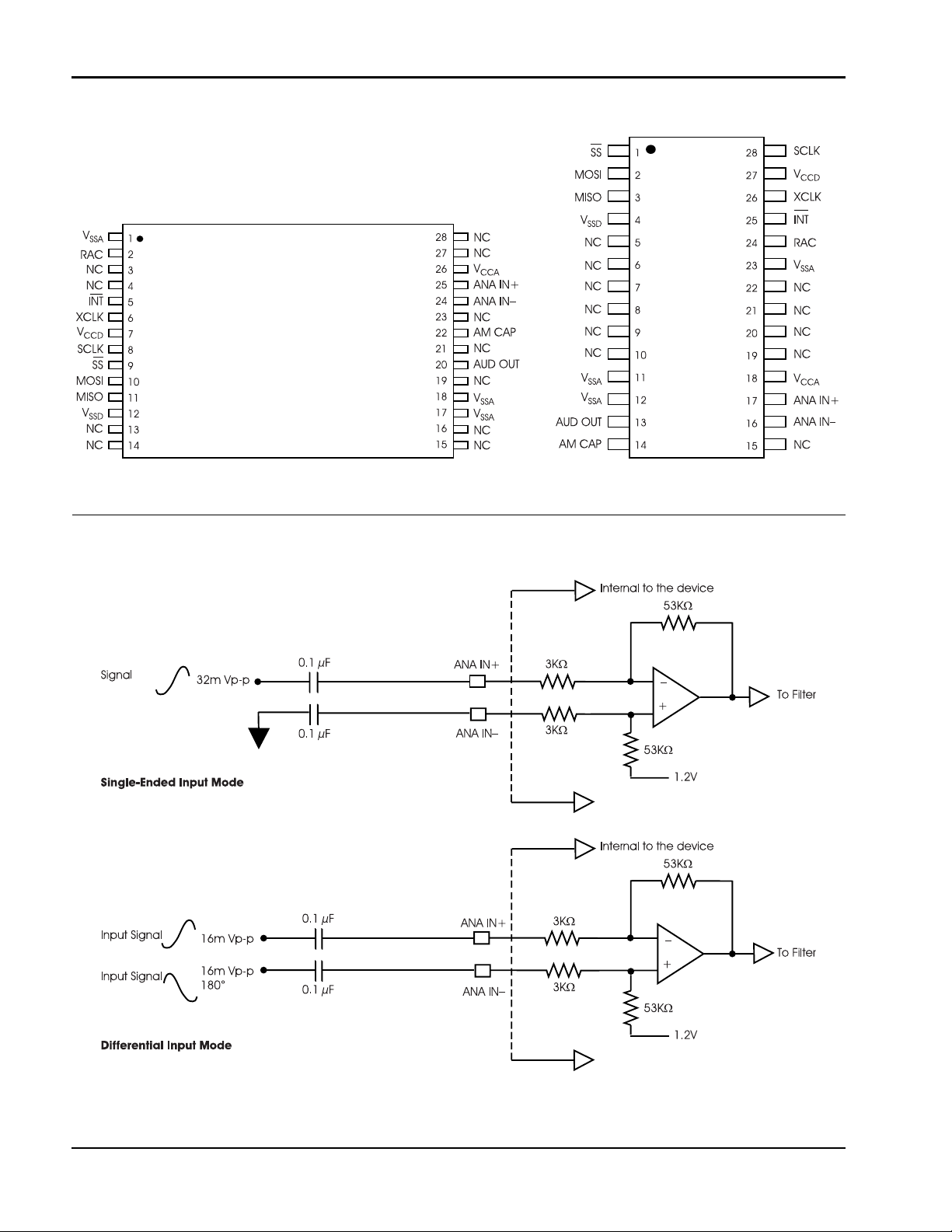
Figure 1: ISD4004 Series TSOP and PDIP/SOIC Pinouts
ISD4004
ISD4004
28-PIN TSOP
Figure 2: ISD4004 Series ANA IN Modes
PDIP/SOIC
2
Voice Solutions in Silicon
™
Page 7

ISD4004 Series
NON-INVERTING ANALOG INPUT (ANA IN+)
This pin is the non-inverting ana log input that transfers the signal to the device for recording. The analog input amplifier can be dr iven single ended or
differentially. In the single-ended input mode, a
32 mVp-p (peak-to-peak) maximum sign al sh ou ld
be capacitively conn ect ed t o this pin for opt im al
signal quality. This capacitor value, together with
the 3 KW input impedance of AN A IN+, is selected
to give cutoff at the low frequency end of the
voice passband. In the differential-input mode,
the maximum input signal at ANA IN+ should be
16 mVp-p for optimal signal quality. The circuit
connections for the two modes a re shown in Figure 2 on page 2.
INVERTING ANALOG INPUT (ANA IN–)
This pin is the inverting analog input that transfers
the signal to the device for recording in the differential-input mode. In this differential-input mode,
a 16 mVp-p maximum input signal at ANA IN–
should be capacitively coupled to this pin for optimal signal quality as shown in the ISD4004 Series
ANA IN Modes, Figure 2. This capacitor value
should be equal to the coupling capacitor used
on the ANA IN+ pin. The input impedance at ANA IN–
is nominally 56 KW. In the single-ended mode, ANA
IN– should be capacitively coupled to V
SSA
through a capacitor equal to that used on the
ANA IN+ input.
AUDIO OUTPUT (AUD OUT)
This pin provides the audio output to the user.
It is capable of driving a 5 KW impedance. It is
recommended that this pin be AC coupled.
NOTE The AUDOUT pin is always at 1.2 volts when
the device is powered up. When in playback, the output buffer connected to this
pin can drive a load as small as 5 K
When in record, a resistor c onnects AUDOUT to the internal 1.2 volt analog ground
supply. This resistor is approximately
W, but will vary somewhat according
850 K
to the sample rate of the device. This relatively high impedance allows this pin to
be connected to an audio bus without
loading it down.
W.
SLAVE SELECT (SS)
This input, when LOW, will select the ISD4004
device.
MASTER OUT SLAVE IN (MOSI)
This is the serial input to the ISD4004 device. The
master microcontroller places data on the MOSI
line one half-cycle before the rising clock edge to
be clocked in by the ISD4004 device.
MASTER IN SLAVE OUT (MISO)
This is the serial outp ut of th e ISD400 4 de vice . This
output goes into a high-impedance state if the
device is not selecte d .
SERIAL CLOCK (SCLK)
This is the clock input to the ISD4004. It is generated by the master device (microcontroller) and is
used to synchronize data transfers in and out of
the device through the MISO an d MOSI lines. Dat a
is latched into the IS D4004 on the rising edge of
SCLK and shif ted out of the de vice on the f alling
edge of SCLK.
INTERRUPT (INT)
The ISD4004 interrupt pin goes LOW and stays LOW
when an Overflow (OVF) or End of Message (EOM)
marker is detected. This is an open drain output
pin. Each operati on that ends in an EOM or Ov er flow will generate an interrupt includin g the message cueing cycles. T he interrupt will b e cleared
the next time an SPI cycle is initiated. The interrupt
status can be read by an RINT instruction.
Overflow Flag (OVF)—The Overflow flag indicates that the end of the IS D4004 ’s ana log me mory has been reached during a record or
playback operation.
End of Message (EOM)—The End-of-Message
flag is set only during playback operation whe n an
EOM is found. There are eight EOM flag position
options per row.
ISD
3
Page 8
ISD4004 Series
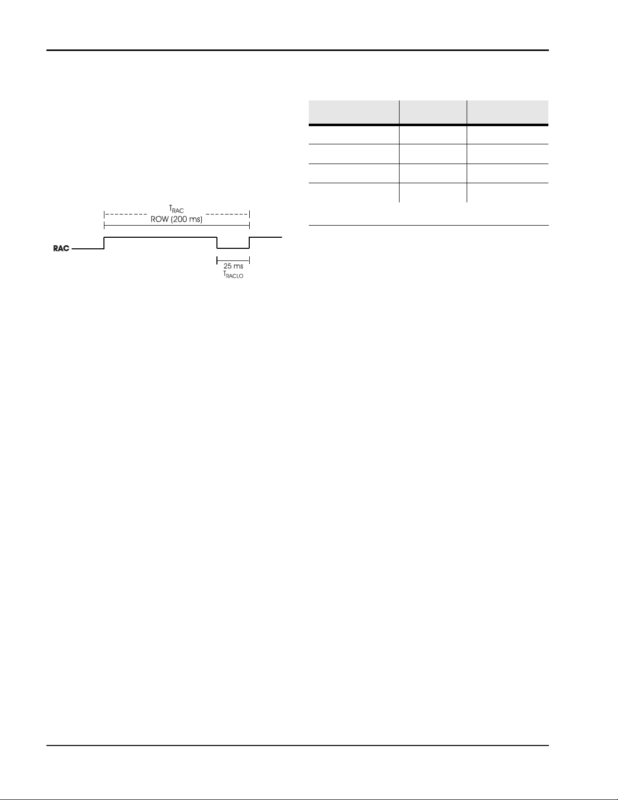
ROW ADDRESS CLOCK (RAC)
This is an open dr ain output pin t hat provides a s ignal with a 200 ms pe riod at the 8 KHz sampling fr equency. (This represents a single row of memory
and there are 2400 rows o f memory in the I SD4004
series devices.) This signal stays HIGH for 175 ms
and stays LOW for 25 ms when it reaches the end
of a row.
The RAC pin stays HIGH for 109.38 msec and stays
LOW for 15.63 msec in Message Cueing mode
(see page 5 for a more detailed description of
Message Cueing). Refer to the AC Parameters table for RAC timing information on other sample
rate products.
When a record command is first initiated, the RAC
pin remains HIGH for an extr a T
period. This is
RACLO
due to the need to load sample and hold circui ts
internal to the device. This pin can be used for
message management techni ques.
EXTERNAL CLOCK INPUT (XCLK)
The external cl ock input for t he ISD4004 pr oducts
has an internal pull-down device. These products
are configured at the factory with an internal sampling clock frequency centered to ±1 percen t of
specification. The frequency is then maintained to
a variation ov er the enti re commerc ial tempera ture and operating voltage ranges as defined by
the minimum/maximum limits in the applicable
AC Parameters table. The internal clock has a tolerance, over the extended temperature, industrial
te mp e ra tu r e a nd vo ltag e ran ges as def ined by the
minimum/maximum limits in the applicable AC
Parameters table. A regulated power supply is
recommended for industrial temperature range
parts. If greater precision is required, the device
can be clocked through the XCLK pin in Table 1.
Table 1: External Clock Input Clocking
Tabl e
Part Number Sample Rate Required Clock
ISD4004-08M 8.0 KHz 1024 KHz
ISD4004-10M 6.4 KHz 819.2 KHz
ISD4004-12M 5.3 KHz 682.7 KHz
ISD4004-16M 4.0 KHz 512 KHz
These recommended clock rates should not be
varied because the antialiasing and smoothing filters
are fixed. Thus, aliasing problems can occur if the
sample rate d iff er s f rom the o ne re comme nd ed.
The duty cycle on the input clo ck i s not critical, as
the clock is immediately divided by two internal l y.
If the XCLK is not used, this input should be
connected to ground.
AUTOMUTE™ FEATURE (AM CAP)
This pin is used in controlling the AutoMute feature.
The AutoMute feature attenuates the signal when
it drops below an internally set threshold. This helps
to eliminate noise (with 6 dB of attenuation) when
there is no signal (i.e., during periods of silence). A
1 mF capacitor to ground should be connected to
the AM CAP pin. Thi s capacitor b ecomes a pa rt of
an internal peak detector which senses the signal
amplitude (peak). This peak level is compared to
an internally set threshold to determine the AutoMute trip point . For larg e si gnals t he A utoMu te attenuation is set to 0 dB while 6 dB of attenuation
occurs for silence. The 1 mF capacitor al so affe ct s
the rate at which the AutoMute feature changes
with the signal amplitude (or the attack time). The
Automute feature c an be disabled by connecting
the AM CAP pin to V
CCA
.
4
Voice Solutions in Silicon
™
Page 9

SERIAL PERIPHERAL INTERFACE (SPI) DESCRIPTION
ISD4004 Series
The ISD4004 series operates from an SPI serial interface. The SPI interface operates with the following
protocol.
The data tra nsfer protocol assumes that the microcontroller’s SPI shift registers are clocked on the
falling edge of the SCLK. With the ISD4004, data is
clocked in on the MOSI pin on the rising clock
edge. Data is clocked out on the MISO pin on the
falling clock edge.
1. All serial data transfers begin with the fa lling
edge of SS
is held LOW during all serial communica-
2. SS
tions and held HIGH between instructions.
3. Data is clocked in on the rising clock edge
and data is clocked out on the falling clo ck
edge.
4. Play and Record oper ations are initi ated by
enabling the device by as serti ng the SS
LOW, shifting in an opcode and an address
field to the ISD4004 device (refer to the Opcode Summary on the page 6).
pin.
pin
read interrupt data and start a new operation within the same SPI cycle.
8. An operation begins with the RUN bit set
and ends with the RUN bit reset.
9. All operations begin with the rising edge
of SS
.
MESSAGE CUEING
Message cueing allows the user to skip through
messages, without k nowing the actu al physical lo cation of the message. This operation is used during playback. In this mode, the messages are
skipped 1600 times faster than in normal playback mode. It will stop when an EOM marker is
reached. Then, the internal address counter will
point to the next message.
5. The opcodes and address fields are as follows: <8 control bits> and <16 address
bits>.
6. Each operation that ends in an EOM or
Overflow will generate a n interrup t, includ ing the Message Cuein g cycles. The Inte rrupt will be cleared the next time an SPI
cycle is initiated.
7. As Interrupt data is shifted out of the
ISD4004 MISO pin, control and address
data is simultaneously being shifted into
the MOSI pin. Care should be taken such
that the data shifted in is comp atible with
current system operation. It is possible to
ISD
5
Page 10

ISD4004 Series
Table 2:Opcode Summary
Instruction
POWERUP 00100XXX Power-Up: Device will be ready for an operation after T
SETPLAY 11100XXX <A15–A0> Initiates Playback from address <A15–A0>.
PLAY 11110XXX Playback from the current address (until EOM or OVF).
SETREC 10100XXX <A15–A0> Initiates a Record operation from address <A15–A0>.
REC 10110XXX Records from current address until OVF is reached.
SETMC 11101XXX <A15–A0> Initiates Message Cueing (MC) from address <A15–A0>.
1
MC
STOP 0X110XXX Stops current operation.
STOPPWRDN 0X01XXXX Stops current Operation and enters stand-by (power-down) mode.
2
RINT
1. Message Cueing can be selected only at the
beginning of a play operation.
11111XXX Performs a Message Cue. Proceeds to the en d of the current
0X110XXX Read Interrupt status bits: Overflow and EOM.
Opcode <8 bits>
Address <16 bits>
Operational Summary
.
PUD
message (EOM) or enters OVF condition if no more messages are
present.
2. As the Interrupt data is shifted out of the ISD4004,
control and address data is being shifted in. Care
should be taken such that the data shifted in is
compatible with current system operation. It is
possible to read interrupt data and start a new
operation at the same time. See Figure 5 through
Figure 8 for Opcode format.
POWER-UP SEQUENCE
The ISD4004 will be ready for an operation after
T
(25 ms approximately for 8 KHz sample rate).
PUD
The user needs to wait T
tional command. For example, to play from address 00 the following programing cycle should be
used.
Playback Mode
1. Send POWERUP command.
2. Wait T
(power-up delay).
PUD
3. Send SETPLAY command with address 00.
4. Send PLAY command.
The device will start pla ybac k at addr ess 00 and it
will generate an interrupt when an EOM is
reached. It will then stop playback.
before issuing an opera-
PUD
Record Mode
1. Send POWERUP command.
2. Wait T
(power-up delay).
PUD
3. Send POWERUP command.
4. Send SETREC command with address 00.
5. Send REC command.
The device will start recording at addr ess 00 and it
will generate an interrupt when an overflow is
reached (end of memory array). It wi ll then stop recording.
6
Voice Solutions in Silicon
™
Page 11

ISD4004 Series
SPI PORT
The following diagram describes the SPI port and the control bits associated with it.
Figure 3: SPI Port
SPI CONTROL REGISTER
The SPI control register provides control of individual device functions such as Play, Rec ord, Message
Cueing, Power-Up and Power-Down, Start and Stop operations, and Ignore Address pointers.
Table 3: SPI Control Register
Control
Register
RUN Enable or Disable an operation PU Master power control
P/R Selects Play or Record operation IAB Ignore address control bit
MC Enable or Disable Message Cueing P15–P0 Output of the row pointer register
Bit Device Function
==1
==1
==1
Start
0
Stop
Play
0
Record
Enable Message Cueing
0
Disable Message Cueing
Control
Register
A15–A0 Input address regi s ter
Bit Device Function
==10Power-Up
Power-Down
==10Ignore input address register (A15–A0)
Use the input address register contents
for an operation (A15–A0)
ISD
7
Page 12

ISD4004 Series
Figure 4: SPI Interface Simplified Block Diagram
Table 4: Absolute Maximum Ratings
(Packaged Parts)
Condition Value
Junction temperature 150°C
Storage temperature range –65°C to +150°C
Voltage applied to any pi n (VSS – 0.3 V) to
Voltage applied to MOS I , SCLK,
INT, RAC and SS pins (i nput cu rrent
limited to ± 20mA
Lead temperature
(soldering – 10 seconds)
– V
V
CC
SS
1. Stresses above those listed may cause permanent
damage to the device. Exposure to the absolute
maximum ratings may affect device reliability.
Functional operation is not implied at these
conditions.
(1)
(VCC+ 0.3 V)
(VSS – 1.0 V) to
5.5V
300°C
–0.3 V to +7.0 V
Table 5: Operating Conditions
(Packaged Parts)
Condition Va lue
Commercial operating
temperature range
(1)
Extended operating
temperature
(1)
Industrial operating
= V
CCA
SSA
(1)
= V
= V
(2)
(3)
CCD.
SSD
temperature
Supply voltage (VCC)
Ground voltage (VSS)
1. Case temperature.
2. V
CC
3. VSS = V
.
0°C to +70°C
–20°C to +70°C
–40°C to +85°C
+2.7 V to +3.3 V
0 V
8
Voice Solutions in Silicon
™
Page 13

ISD4004 Series
Table 6: DC Parameters (Packaged Parts)
Symbol Parameters Min
V
V
V
V
V
I
IL
IH
OL
OL1
OH
CC
Input Low Voltage VCCx0.2 V
Input High Voltage VCCx0.8 V
Output Low Voltage 0.4 V IOL = 10 µA
RAC, INT Output Low Voltage 0.4 V IOL = 1 mA
Output High Voltage VCC–0.4 V IOH = –10 µA
VCC Current (Operating)
— Playback
— Record
I
SB
I
IL
I
HZ
R
EXT
R
ANA IN+
R
ANA IN–
A
ARP
VCC Current (Standby) 1 10 µA
Input Leakage Current ±1 µA
MISO Tristate Current 1 10 µA
Output Load Impedance 5 KW
ANA IN+ Input Resistance 2.2 3.0 3.8 KW
ANA IN– Input Resistance 40 56 71 KW
ANA IN+ or ANA IN– to AUD OUT Gain 25 dB
(2)
Typ
(1)
15
25
Max
(2)
30
40
Units Conditions
mAmAR
EXT
R
EXT
(3) (4)
(5)
= ¥
= ¥
(3)
(3)
1. Typical values: TA = 25°C and 3.0 V.
2. All min/max limits are guaranteed by ISD via electrical testing or characterization. Not all specifications are
100 percent tested.
3. V
4. SS
5. Measured with AutoMute feature disabled.
CCA
= V
and V
CCA
connected together.
CCD
= V
, XCLK = MOSI = V
CCD
SSA
= V
and all other pins floating.
SSD
Table 7: AC Parameters (Packaged Parts)
Symbol Characteristic Min
F
S
Sampling
Frequency
ISD4004-08M
ISD4004-10M
ISD4004-12M
ISD4004-16M
F
CF
Filter Pass Band ISD4004-08M
ISD4004-10M
ISD4004-12M
ISD4004-16M
T
REC
Record Duration ISD4004-08M
ISD4004-10M
ISD4004-12M
ISD4004-16M
(2)
Typ
(1)
8.0
6.4
5.3
4.0
3.4
2.7
2.3
1.7
10
12
16
(2)
Max
8
Units Conditions
(5)
KHz
(5)
KHz
(5)
KHz
(5)
KHz
KHz
3-dB Roll-Off Point
KHz
3-dB Roll-Off Point
KHz
3-dB Roll-Off Point
KHz
3-dB Roll-Off Point
(6)
min
(6)
min
(6)
min
(6)
min
(3) (7)
(3) (7)
(3) (7)
(3) (7)
ISD
9
Page 14

ISD4004 Series
Table 7: AC Parameters (Packaged Parts)
Symbol Characteristic Min
T
PLAY
Playback Duration ISD4004-08M
ISD4004-10M
ISD4004-12M
ISD4004-16M
T
PUD
Power-Up Delay ISD4004-08M
ISD4004-10M
ISD4004-12M
ISD4004-16M
T
or
STOP
T
PAUSE
Stop or Pause in
Record or Play
ISD4004-08M
ISD4004-10M
ISD4004-12M
ISD4004-16M
T
RAC
RAC Clock Period ISD4004-08M
ISD4004-10M
ISD4004-12M
ISD4004-16M
T
RACLO
RAC Clock Low
Time
ISD4004-08M
ISD4004-10M
ISD4004-12M
ISD4004-16M
(2)
Typ
10
12
16
25
31.25
37.5
50
50
62.5
75
100
200
250
300
400
25
31.25
37.5
50
(1)
(2)
Max
8
Units Conditions
min
min
min
min
(6)
(6)
(6)
(6)
msec
msec
msec
msec
msec
msec
msec
msec
msec
msec
msec
msec
(10)
(10)
(10)
(10)
msec
msec
msec
msec
T
RACM
T
RACML
RAC Clock Period
in Message
Cueing Mode
RAC Clock Low
Time in Message
Cueing Mode
ISD4004-08M
ISD4004-10M
ISD4004-12M
ISD4004-16M
ISD4004-08M
ISD4004-10M
ISD4004-12M
ISD4004-16M
125
156.3
187.5
250
15.63
19.53
23.44
31.25
µsec
µsec
µsec
µsec
µsec
µsec
µsec
µsec
THD Total Harmon i c Distortio n 1 2 % @ 1 KHz
V
IN
1. Typical values: TA = 25°C and 3.0 V.
2. All min/max limits are guaranteed by ISD via electrical testing or characterization. Not all specifications are 100 percent
tested.
3. Low-frequency cut off depends upon the value of external capacitors (see Pin Descriptions).
4. Single-ended input mode. In the differential input mode, V
5. Sampling Frequency can vary as much as ±2.25 percent over the commercial temperature, and voltage ranges,
and –6/+4 percent over the extended temperature, industrial temperature and voltage ranges. For greater
stability, an external clock can be utilized (see Pin Descriptions).
6. Playback and Record Duration can vary as much as ±2.25 percent over the commercial temperature and voltage
ranges, and –6/+4 percent over the extended temperature, industrial temperature and voltage ranges. For
greater stability, an external clock can be utilized (see Pin Descriptions).
7. Filter specification applies to the antialiasing filter and the smoothing filter. Therefore, from input to output, expect a
6dB drop by nature of passing through both filters.
8. The typical output voltage will be approximately 570mVp-p with V
9. For optimal signal quality, this maximum limit is recommended.
10. When a record command is sent, T
ANA IN Input Voltage 32 mV Peak-to-Peak
maximum for ANA IN+ and ANA IN– is 16mVp-p.
IN
at 32mVp-p.
IN
RAC=TRAC+TRACLO
on the first row addressed.
(4) (8) (9)
10
Voice Solutions in Silicon
™
Page 15

ISD4004 Series
Table 8: Absolute Maximum Ratings (Die)
(1)
Condition Value
Junction temperature 150°C
Storage temperature range –65°C to +150°C
Voltage applied to any pa d (VSS – 0.3 V) to
(VCC + 0.3 V)
Voltage appl ied t o MO SI, SCL K, I NT,
RAC and SS pins (input current
(VSS – 1.0 V) to
5.5 V
limited to ± 20mA
VCC – V
1. Stresses above those listed may cause permanent
SS
damage to the device. Exposure to the absolute
maximum ratings may affect device reliability.
Functional operation is not implied at these conditions.
–0.3 V to +7.0 V
Table 10: DC Parameters (Die)
Symbol Parameters Min
Table 9: Operating Conditions (Die)
Condition Value
Commercial operating
temperature range
Supply voltage (V
CC
Ground voltage (V
1. VCC = V
2. VSS = V
(2)
Typ
SSA
(1)
CCA
= V
= V
(1)
)
(2)
)
SS
CCD
SSD
Max
.
(2)
0°C to +50°C
+2.7 V to +3.3 V
0 V
Units Conditions
V
IL
V
IH
V
OL
V
OL1
V
OH
I
CC
I
SB
I
IL
I
HZ
R
EXT
R
ANA IN+
R
ANA IN–
A
ARP
1. Typical values: TA = 25°C and 3.0 V.
2. All min/max limits are guaranteed by ISD via electrical testing or characterization. Not all specifications are
100 percent tested.
3. V
4. SS
5. Measured with AutoMute feature disabled.
Input Low Voltage VCCx0.2 V
Input High Voltage VCCx0.8 V
Output Low Voltage 0.4 V IOL = 10 µA
RAC, INT Output Low Voltage 0.4 V IOL = 1 mA
Output High Voltage VCC–0.4 V IOH = –10 µA
VCC Current (Operating)
— Playback
— Record
15
25
30
40
mAmAR
VCC Current (Standby) 1 10 µA
Input Leakage Current ±1 µA
MISO Tristate Current 1 10 µA
Output Load Impedance 5
ANA IN+ Input Resistance 2.2 3.0 3.8
ANA IN– Input Resistance 40 56 71
K
W
K
W
K
W
ANA IN+ or ANA IN– to AUDOUT Gain 25 dB
CCA
= V
and V
CCA
connected together.
CCD
= V
, XCLK = MOSI = V
CCD
SSA
= V
and all other pins floating.
SSD
EXT
R
EXT
(3) (4)
(5)
= ¥
= ¥
ISD
(3)
(3)
11
Page 16

ISD4004 Series
Table 11: AC Parameters (Die)
Symbol Characteristic Min
F
S
Sampling
Frequency
ISD4004-08M
ISD4004-10M
ISD4004-12M
ISD4004-16M
F
CF
Filter Pass Band ISD4004-08M
ISD4004-10M
ISD4004-12M
ISD4004-16M
T
REC
Record Duration ISD4004-08M
ISD4004-10M
ISD4004-12M
ISD4004-16M
T
PLAY
Playback Duration ISD4004-08M
ISD4004-10M
ISD4004-12M
ISD4004-16M
T
PUD
Power-Up Delay ISD4004-08M
ISD4004-10M
ISD4004-12M
ISD4004-16M
(2)
Typ
31.25
37.5
(1)
8.0
6.4
5.3
4.0
3.4
2.7
2.3
1.7
10
12
16
10
12
16
25
50
(2)
Max
8
8
Units Conditions
(5)
KHz
(5)
KHz
(5)
KHz
(5)
KHz
KHz
3dB Roll-Off Point
KHz
3dB Roll-Off Point
KHz
3dB Roll-Off Point
KHz
3dB Roll-Off Point
(5)
min
(5)
min
(5)
min
(5))
min
(5)
min
(5)
min
(5)
min
(5)
min
(3) (6)
(3) (6)
(3) (6)
(3) (6)
msec
msec
msec
msec
T
STOP
T
PAUSE
T
RAC
T
RACLO
T
RACM
T
RACML
or
Stop or Pause in
Record or Play
RAC Clock Period ISD4004-08M
RAC Clock Lo w
Time
RAC Clock Per i od
in Message
Cueing Mode
RAC Clock Lo w
Time in Message
Cueing Mode
ISD4004-08M
ISD4004-10M
ISD4004-12M
ISD4004-16M
ISD4004-10M
ISD4004-12M
ISD4004-16M
ISD4004-08M
ISD4004-10M
ISD4004-12M
ISD4004-16M
ISD4004-08M
ISD4004-10M
ISD4004-12M
ISD4004-16M
ISD4004-08M
ISD4004-10M
ISD4004-12M
ISD4004-16M
50
62.5
75
100
200
250
300
400
25
31.25
37.5
50
125
156.3
187.5
250
15.63
19.53
23.44
31.25
msec
msec
msec
msec
msec
msec
msec
msec
msec
msec
msec
msec
msec
msec
msec
msec
msec
msec
msec
msec
(9)
(9)
(9)
(9)
12
Voice Solutions in Silicon
™
Page 17

Table 11: AC Parameters (Die)
ISD4004 Series
Symbol Characteristic Min
(2)
Typ
(1)
Max
(2)
Units Conditions
THD Total Harmonic Distortion 1 2 % @ 1 KHz
V
IN
1. Typical values: T
2. All min/max limits are guaranteed by ISD via electrical testing or characterization. Not all specifications are 100
percent tested.
3. Low-frequency cut off depends upon the value of external capacitors (see Pin Descriptions).
4. Single-ended input mode. In the differential input mode, V
to-peak.
5. Sampling Frequency and Duration can vary as much as ±2.25 percent over the commercial temperature and
voltage ranges. For greater stability, an external clock can be utilized (see Pin Descriptions).
6. Filter specification applies to the antialiasing filter and to the smoothing filter.
7. The typical output voltage will be approximately 570 mV peak-to-peak with VIN at 32 mV peak-to-peak.
8. For optimal signal quality, this maximum limit is recommended.
9. When a record command is sent, T
ANA IN Input Voltage 32 mV Peak-to-Peak
= 25°C and 3.0 V.
A
maximum for ANA IN+ and ANA IN– is 16 mV peak-
IN
RAC=TRAC+TRACLO
Table 12: SPI AC Parameters
on the first row addressed.
1
(4) (7) (8)
Symbol Characteristics Min Max Units Conditions
T
SSS
T
SSH
T
DIS
T
DIH
T
PD
(2)
T
DF
T
SSmin
T
SCKhi
T
SCKlow
F
0
SS Setup Time 500 nsec
SS Hold Time 500 nsec
Data in Setup Time 200 nsec
Data in Hold Time 200 nsec
Output Delay 500 nsec
Output Delay to hiZ 500 nsec
SS HIGH 1 msec
SCLK High Time 400 nsec
SCLK Low Time 400 nsec
CLK Frequency 1,000 KHz
1. Typical values: T
2. Tristate test condition.
ISD
= 25°C and 3.0 V. Timing measured at 50 percent of the VCC level.
A
13
Page 18

ISD4004 Series
TIMING DIAGRAMS
Figure 5: Timing Diagram
Figure 6: 8-Bit Command Format
14
Voice Solutions in Silicon
™
Page 19

SS
SCLK
ISD4004 Series
Figure 7: 24-Bit Command Format
BYTE 1 BYTE 2 BYTE 3
MOSI
MISO
A0 A1 A2 A3 A4 A5
Figure 8: Playback/Record and Stop Cycle
A6 A7 A8 A9 A10 A11
P4 P5 P6 P7 P8 P9OVF EOM P0 P1 P2 P3 P10
A12 A13 A14 A15
P11
P12 P13 P14 P15
XXX
P16 X X X X X
C1C0
C3 C4
C2
ISD
15
Page 20

ISD4004 Series
Figure 9: Application Example Using SPI
(1)
1. This application example is for illustration purposes only. ISD makes no representation or warranty that such
application will be suitable for production.
2. Please make sure the bypass capacitor, C2 is as close as possible to the package.
16
Voice Solutions in Silicon
™
Page 21

ISD4004 Series
Figure 10: Application Example Using Microwire
1. This application example is for illustration purposes only. ISD makes no representation or warranty that such
application will be suitable for production.
2. Please make sure the bypass capacitor, C2 is as close as possible to the package.
(1)
Figure 11: Application Example Using SPI Port on Microcontroller
1. This application example is for illustration purposes only. ISD makes no representation or warranty that such
application will be suitable for production.
2. Please make sure the bypass capacitor, C2 is as close as possible to the package.
(1)
ISD
17
Page 22

ISD4004 Series
DEVICE PHYSICAL DIMENSIONS
Figure 12: 28-Lead 8x13.4 mm Plastic Thin Small Outline Package (TSOP) Type I (E)
Table 13: Plastic Thin Small Outline Package (TSOP) Type I (E) Dimensions
INCHES MILLIMETERS
Min Nom Max Min Nom Max
A 0.520 0.528 0.535 13.20 13.40 13.60
B 0.461 0.465 0.469 11.70 11.80 11.90
C 0.311 0.315 0.319 7.90 8.00 8.10
D 0.002 0.006 0.05 0.15
E 0.007 0.009 0.011 0.17 0.22 0.27
F 0.0217 0.55
G 0.037 0.039 0.041 0.95 1.00 1.05
H0°3°6°0°3°6°
I 0.020 0.022 0.028 0.50 0.55 0.70
J 0.004 0.008 0.10 0.21
NOTE: Lead coplanarity to be within 0.004 inches.
18
Voice Solutions in Silicon
™
Page 23

Figure 13: 28-Lead 0.600-Inch Plastic Dual Inline Package (PDIP) (P)
ISD4004 Series
Table 14: Plastic Dual Inline Package (PDIP) (P) Dimensions
INCHES MILLIMETERS
Min Nom Max Min Nom Max
A 1.445 1.450 1.455 36.70 36.83 36.96
B1 0.150 3.81
B2 0.065 0.070 0.075 1.65 1.78 1.91
C1 0.600 0.625 15.24 15.88
C2 0.530 0.540 0.550 13.46 13.72 13.97
D0.19 4.83
D1 0.015 0.38
E 0.125 0.135 3.18 3.43
F 0.015 0.018 0.022 0.38 0.46 0.56
G 0.055 0.060 0.065 1.40 1.52 1.65
H 0.100 2.54
J 0.008 0.010 0.012 0.20 0.25 0.30
S 0.070 0.075 0.080 1.78 1.91 2.03
q 0° 15° 0° 15°
ISD
19
Page 24

ISD4004 Series
Figure 14: 28-Lead 0.300-Inch Plastic Small Outline Integrated Circuit (SOIC) (S)
Table 15: Plastic Small Outline Integrated Circuit (SOIC) (S) Dimensions
INCHES MILLIMETERS
Min Nom Max Min Nom Max
A 0.701 0.706 0.711 17.81 17.93 18.06
B 0.097 0.101 0.104 2.46 2.56 2.64
C 0.292 0.296 0.299 7.42 7.52 7.59
D 0.005 0.009 0.0115 0.127 0.22 0.29
E 0.014 0.016 0.019 0.35 0.41 0.48
F 0.050 1.27
G 0.400 0.406 0.410 10.16 10.31 10.41
H 0.024 0.032 0.040 0.61 0.81 1.02
NOTE: Lead coplanarity to be within 0.004 inches.
20
Voice Solutions in Silicon
™
Page 25

Figure 15: ISD4004 Series Bonding Physical Layout1 (Unpackaged Die)
ISD4004 Series
ISD4004 Series
I. Die Dimensions
X: 4230 microns
Y: 9780 microns
II. Die Thickness
(3)
11.5 ±0.5 mils
III. Pad Opening (min)
90 x 90 microns
3.5 x 3.5 mils
V
SSD1
SSD2
MISOV
MOSI
SCLK
V
SS
CCD1
ISD4004
V
CCD2
XCLK
INT
RAC
V
SSA
(2)
V
SSA
V
SSA
1. The backside of die is internally connected to VSS. It MUST NOT be connected to any other potential or damage
may occur.
2. Double bond recommended.
3. This figure reflects the current die thickness. Please contact ISD as this thickness may change in the future.
ISD
AUD OUT
AM CAP
ANA IN–
ANA IN+
V
CCA
(2)
21
Page 26

ISD4004 Series
Pin Pin Name X Axis Y Axis
Table 16: ISD4004 Series Device Pin/Pad Designations,
with Respect to Die Center (µm)
V
SSA
V
SSA
VSS Analog Power Supply –1898.1 –4622.4
VSS Analog Power Supply –1599.9 –4622.4
AUD OUT Audio Output 281.9 –4622.4
AM CAP AutoMute 577.3 –4622.4
ANA IN – Inverting Analog Input 1449.4 –4622.4
ANA IN + Noninverting Analog Input 1603.5 –4622.4
(1)
V
V
CCA
SSA
VCC Analog Power Supply 1898.7 –4622.4
VSS Analog Power Supply 1885.2 –4622.4
RAC Row Address Clock 1483.8 4623.7
INT Interrupt 794.8 4623.7
XCLK External Clock Input 564.8 4623.7
V
CCD2
V
CCD1
VCC Digital Power Supply 387.9 4623.7
VCC Digital Power Supply 169.5 4623.7
SCLK Slave Clock –14.7 4623.7
SS Slave Select –198.1 4623.7
MOSI Master Out Slave In –1063.7 4623.7
MISO Master In Slave Out –1325.6 4623.7
V
SSD1
V
SSD2
1. Double bond recommended.
VSS Digital Power Supply –1655.3 4623.7
VSS Digital Power Supply –1836.9 4623.7
22
Voice Solutions in Silicon
™
Page 27

ORDERING INFORMATION
Product Number Descriptor Key
ISD4004– _ _ _ _ _
ISD4004 Series
Product Family
ISD4000 Family
Product Series
04 = Fourth Series (8–16 min)
Duration:
08M=8 minutes
10M=10 minutes
12M=12 minutes
16M=16 minutes
Special Temperature Field:
Blank= Commercial Packaged (0°C to +70°C)
or Commercial Die (0°C to +50°C)
D = Extended (–20°C to +70°C)
I = Industrial (–40°C to +85°C)
Package Type:
E = 28-Lead 8x13.4mm Plastic Thin Small Outline
Package (TSOP) Type 1
P = 28-Lead 0.600-Inch Plastic Dual Inline Package
(PDIP)
S = 28-Lead 0.300-Inch Plastic Small Outline Package
(SOIC)
X =Die
When ordering ISD4004 series devices, please refer to the following valid part numbers.
Part Number Part Number Part Number Part Number
ISD4004-08ME ISD4004-10ME ISD4004-12ME ISD4004-16ME
ISD4004-08MED ISD4004-10MED ISD4004-12MED ISD4004-16MED
ISD4004-08MEI ISD4004-10MEI ISD4004-12MEI ISD4004-16MEI
ISD4004-08MP ISD4004-10MP ISD4004-12MP ISD4004-16MP
ISD4004-08MS ISD4004-10MS ISD4004-12MS ISD4004-16MS
ISD4004-08MSI ISD4004-10MSI ISD4004-12MSI ISD4004-16MSI
ISD4004-08MX ISD4004-10MX ISD4004-12MX ISD4004-16MX
For the latest product information, access ISD’s worldwide website at http://www.isd.com.
ISD
23
Page 28

IMPORTANT NOTICES
The warranty for each product of ISD (Information Storage
Devices, Inc.), is contained in a written warranty which governs
sale and use of such product. Such warranty is contained in the
printed terms and conditions under which such product is sold, or
in a separate written warranty supplied with the product. Please
refer to such written warranty with respect to its applicability to
certain applications of such product.
These products may be subject to restrictions on use. Please
contact ISD, for a list of the current additional restrictions on
these products. By purchasing these products, the purchaser of
these products agrees to comply with such use restrictions. Please
contact ISD for clarification of any restrictions described herein.
ISD, reserves the right, without further notice, to change the ISD
ChipCorder product specifications and/or information in this
document and to improve reliability, functions and design.
ISD assumes no responsibility or liability for any use of the ISD
ChipCorder products. ISD conveys no license or title, either
expressed or implied, under any patent, copyright, or mask work
right to the ISD ChipCorder products, and ISD makes no
warranties or representations that the ISD ChipCorder products are
free from patent, copyright, or mask work right infringement,
unless otherwise specified.
Application examples and alternative uses of any integrated
circuit contained in this publication are for illustration purposes
only and ISD makes no representation or warranty that such
applications shall be suitable for the use specified.
The 100-year retention and 100K record cycle projections are
based upon accelerated reliability tests, as published in the ISD
Reliability Report, and are neither warranted nor guaranteed by
ISD.
Information contained in this ISD ChipCorder data sheet
supersedes all data for the ISD ChipCorder products published
by ISD prior to September, 1998.
This data sheet and any future addendum to this data sheet is
(are) the complete and controlling ISD ChipCorder product
specifications. In the event any inconsistencies exist between the
information in this and other product documentation, or in the
event that other product documentation contains information in
addition to the information in this, the information contained
herein supersedes and governs such other information in its entirety.
Copyright© 1998, ISD (Information Storage Devices, Inc.) All rights
reserved. ISD is a registered trademark of ISD. ChipCorder is a
trademark of ISD. All other trademarks are properties of their
respective owners.
2727 North First Street
San Jose, California 95134
Tel: 408/943-6666
Fax: 408/544-1787
Part No. 2200998D4004
 Loading...