

Page 1

ISD2100 DATASHEET
ISD2100
Digital ChipCorder
with
Multi Time Programming and Digital Audio Interface
Publication Release Feb 9, 2010
- 1 - Revision 0.51
Page 2

ISD2100 DATASHEET
TABLE OF CONTENTS
1 GENERAL DESCRIPTION .............................................................................................................. 3
2 FEATURES ...................................................................................................................................... 3
3 BLOCK DIAGRAM ........................................................................................................................... 4
4 PINOUT CONFIGURATION ............................................................................................................ 5
5 PIN DESCRIPTION .......................................................................................................................... 6
6 SPI INTERFACE .............................................................................................................................. 7
7 ANALOG AND DIGITAL SIGNAL PATH ........................................................................................ 10
7.1.1 PWM Speaker Driver ..................................................................................................................... 10
7.1.2 Internal Oscillator ......................................................................................................................... 10
8 ISD2100 MEMORY MANAGEMENT ............................................................................................. 10
8.1 MESSAGE MANAGEMENT ....................................................................................................................... 10
8.1.1 Voice Prompts ................................................................................................................................ 10
8.1.2 Voice Macros ................................................................................................................................. 10
8.1.3 GPIO Voice Trigger Mac r os: ........................................................................................................ 11
9 ELECTRICAL CHARACTERISTICS .............................................................................................. 12
9.1 OPERATING CONDITIONS ........................................................................................................................ 12
9.2 AC PARAMETERS ................................................................................................................................... 12
9.2.1 Internal Oscillator ......................................................................................................................... 12
9.2.2 Speaker Outputs ............................................................................................................................. 12
9.3 DC PARAMETERS ................................................................................................................................... 12
9.3.2 SPI Timing ..................................................................................................................................... 13
10 APPLICATION DIAGRAM .......................................................................................................... 15
11 PACKAGE SPECIFICATION ...................................................................................................... 16
11.1 20 LEAD QFN ......................................................................................................................................... 16
12 ORDERING INFORMATION ...................................................................................................... 17
13 REVISION HISTORY .................................................................................................................. 18
Publication Release Feb 9, 2010
- 2 - Revision 0.51
Page 3

ISD2100 DATASHEET
GENERAL DESCRIPTION
1
The ISD2100 is a digital ChipCorder® featuring digital de-compression, comprehensive memory
management, flash storage, and integrated digital audio signal paths. This family utilizes flash
memory to provide non-volatile audio playback with duration up to 30 seconds (based on 8kHz/4bit
ADPCM) for a single-chip solution.
Unlike the MLS ChipCorder series, this device provides higher sampling frequency and a signal path
with SNR equivalent to 12-bit resolution.
The ISD2100 can take digital audio data via SPI interface. When SPI interface is chosen, the sample
rate of the audio data sent must be one of the ISD2100 supported sam pl e rates.
The ISD2100 has built-in speaker driver output.
FEATURES
2
• Duration
o 30 seconds based on 8kHz/4bit ADPCM (ISD2130)
• Audio Management
o Store pre-recorded audio (Voice Prompts) using high quality digital compression
o Use a simple index based command for playback
o Execute pre-programmed macro scripts (Voice Macros) designed to control the configuration
of the device and play back Voice Prompts sequences.
• Sample Rate
o 7 sampling frequencies such as 4, 5.3, 6.4, 8, 12.8, 16 and 32 kHz are available.
• Compression Algorithms
o µ-Law: 6, 7 or 8 bits per sample
o Differential µ-Law: 6, 7 or 8 bits per sample
o PCM: 8, 10 or 12 bits per sample
o Enhanced ADPCM: 2, 3, 4 or 5 bits per sample
o Variable-bit-rate optimized compression. This allows best possible compression given a
metric of SNR and background noise levels.
• Oscillator
o Internal oscillator with internal reference: with ±1% deviation at room temperature.
• Output
o PWM: Class D speaker driver to direct drive an 8Ω speaker or buzzer
• I/Os
o SPI interface: MISO, MOSI, SCLK, SS B for commands and digital audio data
o 6 general purpose I/O pins that share SPI i nterface.
• One 8-bit Volume Controls set by SPI command.
• Operating Voltage: 2.7-3.6V
• Package: green, 20L-QFN
• Temperature Options:
o Industrial: -40°C to 85°C
Publication Release Feb 9, 2010
- 3 - Revision 0.51
Page 4
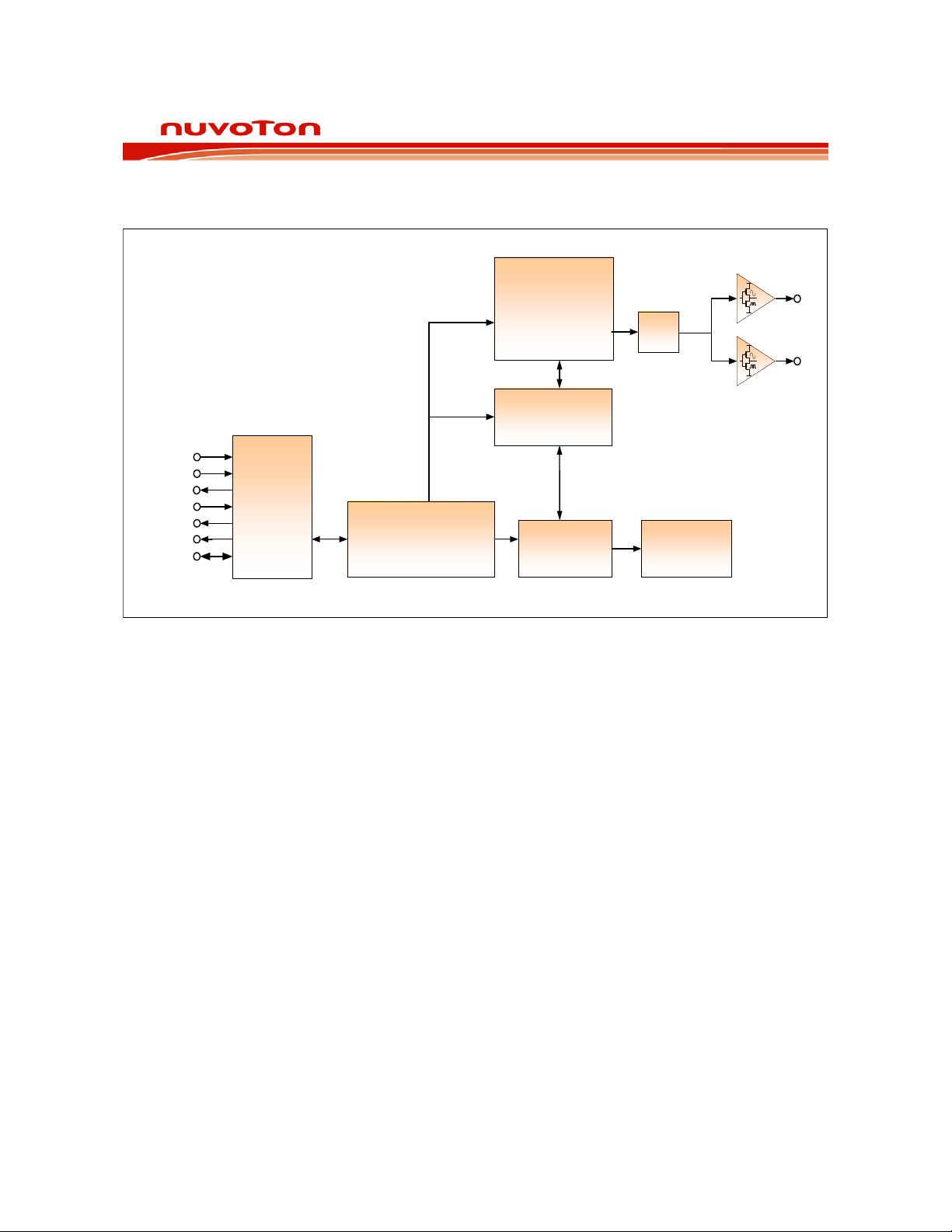
BLOCK DIAGRAM
Digital Signal Path
:
Digital
Filters
Re
-
sampling
Volume Control
PWM Control
De
-
Compression
Flash Memory
Controller
Flash Memory
SPI
&
GPIO
Interface
Memory Management
and Command
Interpreter
SPK
+
SPK
-
SCLK
GPI
1
/
SSB
MISO GPIO
2
/
MOSI GPIO
0
/
INTB GPIO
3
/
RDY
/
BSYB GPIO
4
/
GPIO
5
3
ISD2100 DATASHEET
Figure 3-1 ISD2100 Block Diagram
Publication Release Feb 9, 2010
- 4 - Revision 0.51
Page 5
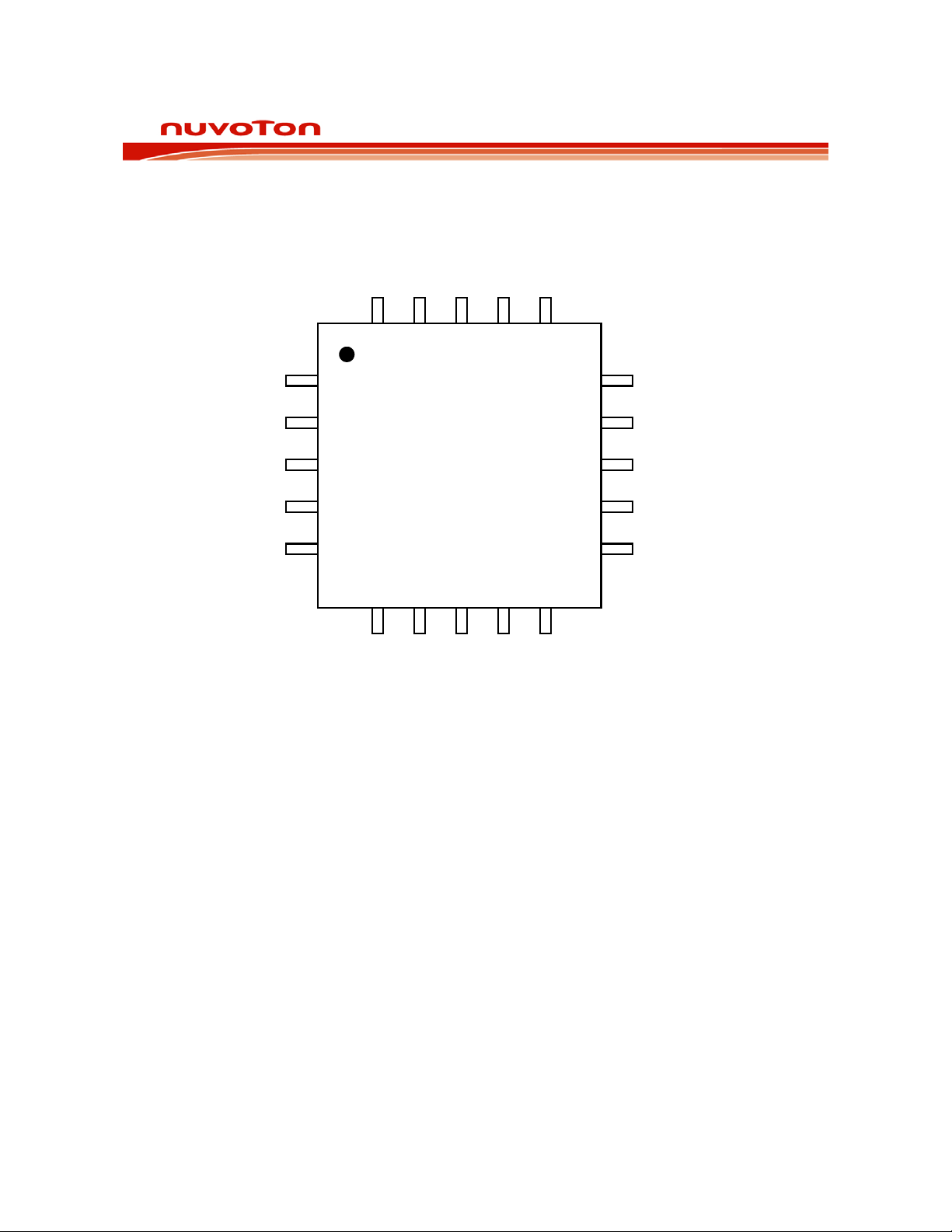
PINOUT CONFIGURATION
2
3
4
5
6 7 8 9 10
1
11
12
13
14
15
1617181920
V
SSD
NC
MOSI / GPIO0
SSB
SCLK / GPI1
MISO / GPIO2
V
CCD
_PWM
V
SSD
_PWM
SPK+
V
CCD
_PWM
INTB / GPIO3
RDY/BSYB / GPIO4
V
CCD
GPIO5
NC
NC
NC
NC
NC
ISD2130
QFN-20
SPK-
4
ISD2100
ISD2100 DATASHEET
Figure 4-1 ISD2100 20-Lead QFN Pin Configurat i on.
Publication Release Feb 9, 2010
- 5 - Revision 0.51
Page 6
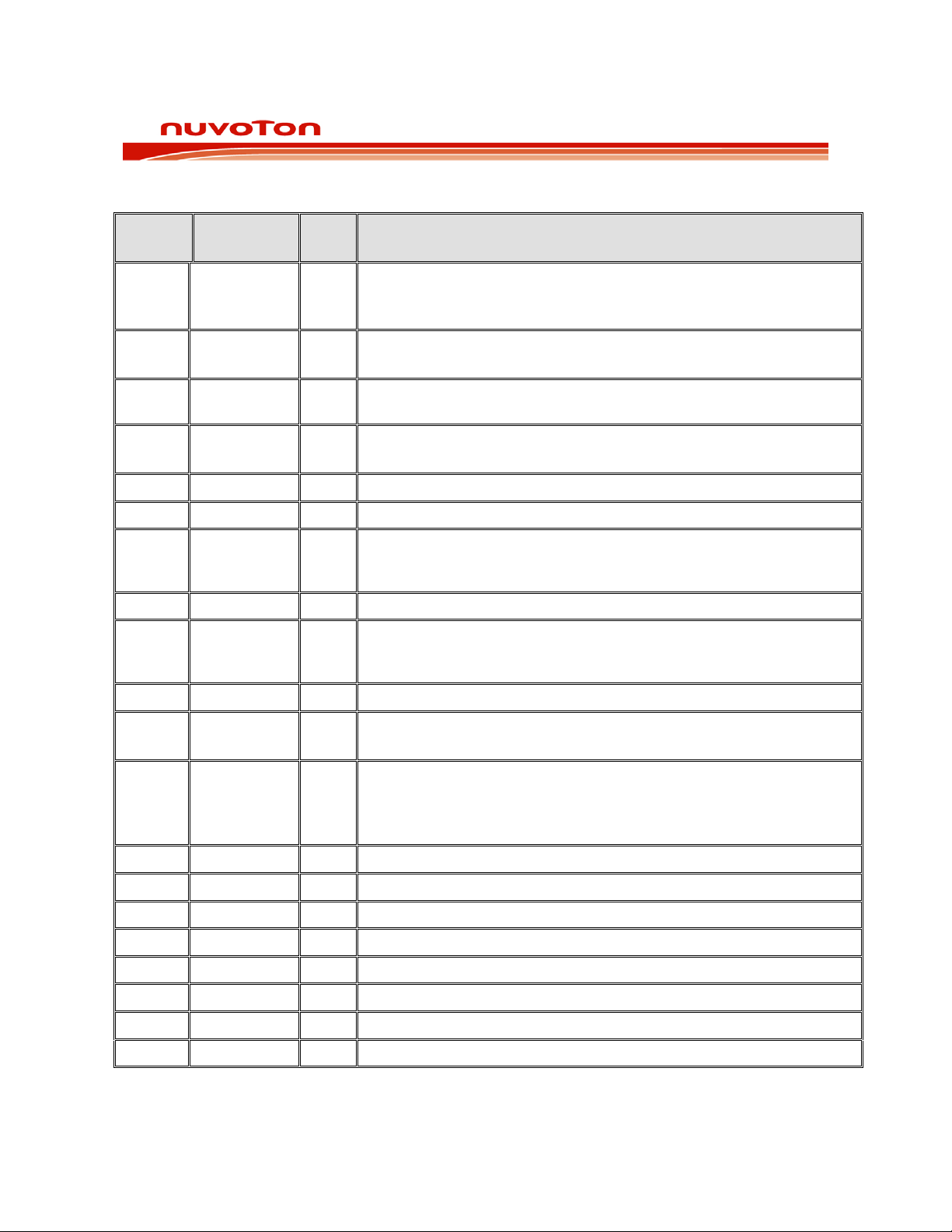
5
PIN DESCRIPTION
ISD2100 DATASHEET
Pin
Pin Name I/O Function
Number
1 MISO /
GPIO2
O Master-In-Slave-Out. Serial output from the ISD2100 to the host. This
pin is in tri-state when SSB=1.
Can be configured as a general purpose I/ O pin.
2 SCLK / GPI1 I Serial Clock input to the ISD2100 from the host.
Can be configured as a general purpose input pi n.
3 SSB I Slave Select input to the ISD2100 from the host. When SSB is low
device is selected and responds to commands on the SPI interface.
4 MOSI /
GPIO0
5 V
6 V
I Digital Ground.
SSD
_PWM I Digital Power for the PWM Driver.
CCD
I Master-Out-Slave-In. Serial input to the ISD2100 from the host.
Can be configured as a general purpose I/O pin.
7 SPK+ O PWM driver positiv e output. This SPK+ output, together with SPK- pin,
provide a differential output to drive 8Ω speaker or buzzer. During
power down this pin is in tri-state.
8 V
_PWM I Digital Ground for the PWM Driver.
SSD
9 SPK- O PWM driver negativ e output. This SPK- output, together with SPK+
pin, provides a differential output to drive 8Ω speaker or buzzer.
During power down this pin is tri-state.
10 V
11 INTB /
12 RDY/BSYB /
_PWM I Digital Power for the PWM Driver.
CCD
O Active low interrupt request pin. This pin is an open-drain output.
GPIO3
Can be configured as a general purpose I/ O pin.
O An output pin to report the status of data transfer on the SPI interface.
GPIO4
“High” indicates that ISD2100 is ready to accept new SPI commands
or data.
Can be configured as a general purpose I/ O pin.
13 NC This pin should be left unconnected.
14 V
I Digital Power.
CCD
15 GPIO5 I/O General purpose I/O pin.
16 NC This pin should be left unconnected.
17 NC This pin should be left unconnected.
18 NC This pin should be left unconnected.
19 NC This pin should be left unconnected.
20 NC This pin should be left unconnected.
Publication Release Feb 9, 2010
- 6 - Revision 0.51
Page 7
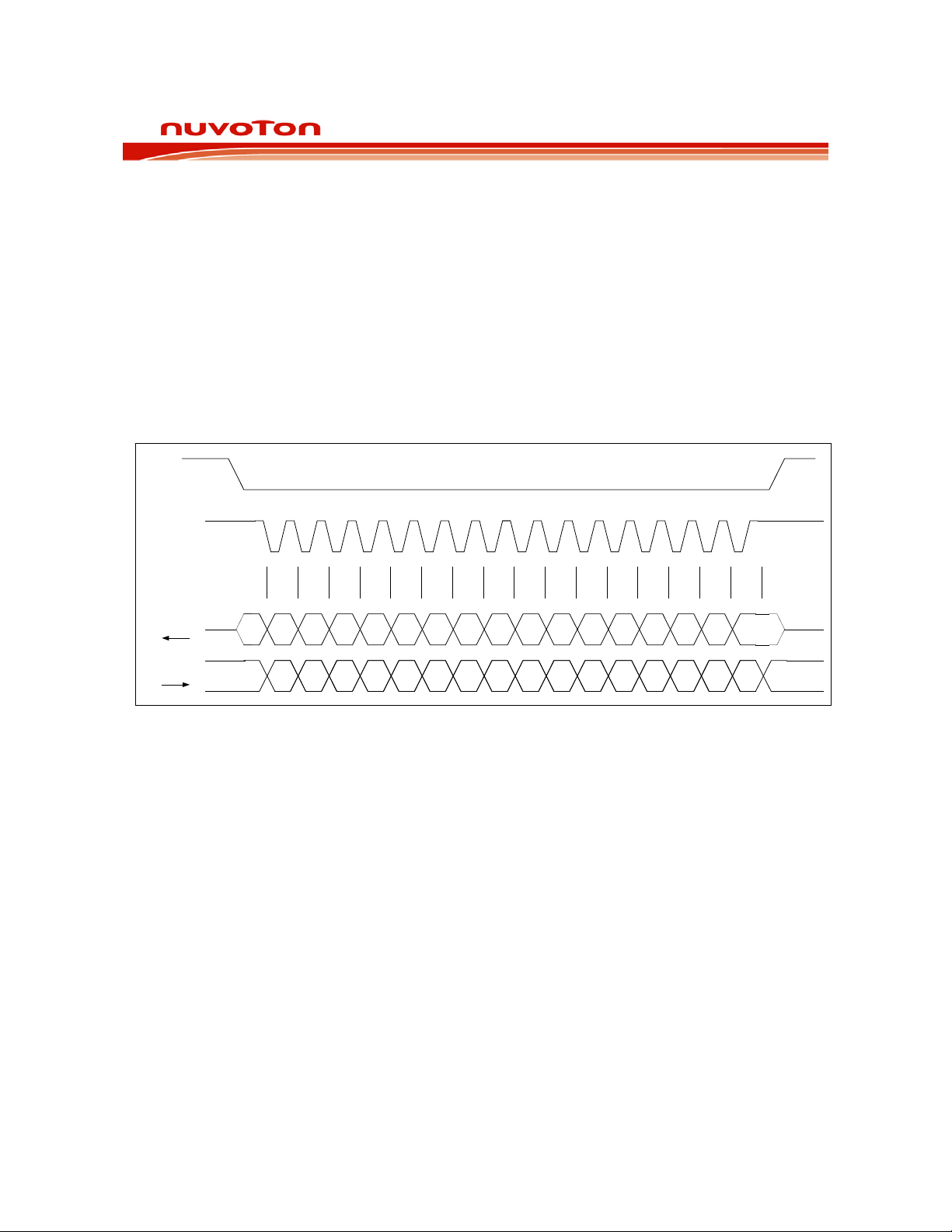
ISD2100 DATASHEET
0 1 2 3 4 5 6 7 0 1
2 3 4 5 6 7
SSB
SCLK
MISO
MOSI
XC7 C6 C5X C4 C3 C2 C1 C0
S7 S6 S5 S4 S3 S2 S1 S0 D7 D6 D5 D4 D3 D2 D1 D0
D7 D6 D5 D4 D3 D2 D1 D0
Z X
SPI INTERFACE
6
This is a standard four-wire interface used for communication between ISD2100 and the host. It
consists of an active low slave-select (SSB), a serial clock (SCLK), a data input (Master Out Slave In MOSI), and a data output (Master In Slave Out - MISO). In addition, for some transactions requiring
data flow control, a RDY/BSYB signal (pin) is available.
The ISD2100 supports SPI mode 3: (1) SCLK must be high when SPI bus is inactive, and (2) data is
sampled at SCLK rising edge. A SPI transaction begins on the falling edge of SSB and its waveform is
illustrated below:
Figure 6-1 SPI Data Transaction.
A transaction begins with sending a command byte (C7-C0) with the most significant bit (MSB – C7)
sent in first. During the byte transmission, the status (S7-S0) of the device is sent out via the MISO
pin. After the byte transmission, depending upon the command sent, one or more bytes of data will be
sent via the MISO pin.
RDY/BSYB pin is used to handshake data into or out of the device. Upon completion of a byte
transmission, RDY/BSYB pin could change its state after the rising edge of the SCLK if the built-in 32byte data buffer is either full or empty. At this point, SCLK must remain high until RDY/BSYB pin
returns to high, indicating that the ISD2100 is ready for the next data transmission. See below for
timing diagram.
Publication Release Feb 9, 2010
- 7 - Revision 0.51
Page 8

ISD2100 DATASHEET
0 1 2 3 4 5 6 7 0 1
2 3 4 5 6 7
SSB
SCLK
MISO
MOSI
XC7 C6 C5X C4 C3 C2 C1 C0
PD RDY INT FULL X
VG
BSY
BUF
FUL
CMD
BSY
PD RDY INT FULL X
VG
BSY
BUF
FUL
CMD
BSY
D7 D6 D5 D4 D3 D2 D1 D0
Z X
RDY/BSYB
BRT/
=1 =1
Figure 6-2 RDY/BSYB Timing for SPI Writing Transactions.
If the SCLK does not remain high, RDY bit of the status register will be set to zero and be reported via
the MISO pin so the host can take the necessary actions (i.e., terminate SPI transmission and retransmit the data when the RDY/BSYB pin returns to high).
For commands (i.e., DIG_READ, SPI_PCM_READ) that read data from ISD2100, MISO is used to
read the data; therefore, the host must monitor the status via the RDY/BSYB pin and take the
necessary actions.
The INT pin will go low to indicate (1) data overrun/overflow when sending data to the ISD2100; or (2)
invalid data from ISD2100. See Figure 6-3 for the timing diagram.
Publication Release Feb 9, 2010
- 8 - Revision 0.51
Page 9

ISD2100 DATASHEET
0 1 2 3 4 5 6 7 0 1
2 3 4 5 6 7
SSB
SCLK
MISO
MOSI
XC7 C6 C5X C4 C3 C2 C1 C0
PD RDY INT FULL X
VG
BSY
BUF
FUL
CMD
BSY
PD RDY INT FULL X
VG
BSY
BUF
FUL
CMD
BSY
D7 D6 D5 D4 D3 D2 D1 D0
Z X
RDY/BSYB
BR
T
/
=1 =0
INT
Figure 6-3 SPI Transaction Ignoring RDY/BSYB
Publication Release Feb 9, 2010
- 9 - Revision 0.51
Page 10

ISD2100 DATASHEET
ANALOG AND DIGITAL SIGNAL PATH
7
7.1.1 PWM Speaker Driver
PWM driver output pins SPK-, together with SPK+ pin, provides a differential output to drive 8Ω
speaker or buzzer. During power down these pins are in tri-state.
7.1.2 Internal Oscillator
The ISD2100 device has an internal oscillator that requires no external resistor to operate, however
the ISD2100 also provide an internal oscillator with external reference resistor (Rosc) that has an
accuracy of ±5% with selectable master sample rate 4Khz, 5.33Khz, 6.4khz, 8Khz, 12.8Khz, 16Khz,
and 32Khz.
ISD2100 MEMORY MANAGEMENT
8
The ISD2100 employs several memory management techniques to make audio playback transparent
to the host controller. The address space of the ISD2100 starts at address zero of the internal
memory.
8.1 MESSAGE MANAGEMENT
The message management schemes implemented on the ISD2100 are:
1. Voice Prompts: A collection of pre-recorded audio that can be played back using the
PLAY_VP SPI command or Voice Macros.
2. Voice Macros: A powerful voice script allowing users to create custom macros to play Voice
Prompts, insert silence and configure the device. Voice Macros are executed with a single SPI
command.
3. User Data: Memory sectors defined and allocated by the users for use in other applications
8.1.1 Voice Prompts
Voice prompts are pre-recorded audio of any length, from short words, phrases or sound
effects to long passages of music. These Voice Prompts can be played back in any order as
determined by the users and applications. A Voi ce Prompt consists of two components:
1. An index pointing to the pre-recorded audio
2. Pre-recorded audio
8.1.2 Voice Macros
Voice Macros are a powerful voice script that allows users to customize their own play
patterns such as play Voice Prompts, insert silence, change the master sample clock, powerdown the device and configure the signal path, i ncluding gain and volume control.
Publication Release Feb 9, 2010
- 10 - Revision 0.51
Page 11

ISD2100 DATASHEET
8.1.3 GPIO Voice Trigger Macros:
The ISD2100 GPIO flexibility allows the user to configure the device to triggers a voice macro in many
different combinations for a push button application. Below is some possible configuration of the GPIO
pins using Voice trigger macros?
1. Single Hi-Low trigger sequence through messages
A high to low trigger on any GPIO 0~ 5 will start to play Voice Macro 3, 4, 5, 6 and back to Voice
Macro 3. Each Voice Macro points directly or indi rectly to voice prompt One, Two, Three, Four.
2. Single Hi-Low trigger Loop unless interrupted by another Trigger
A single trigger on any GPIO 0~ 5 will loop through several messages until it is interrupted by another
trigger to stop playback, the device goes to pow er down after.
3. Single Hi-Low trigger through messages uninterruptable by another Trigger
A single trigger on any GPIO 0~ 5 will sequence through several messages until all messages are
played. The playback cannot be interrupted by another trigger on any GPIO 0~ 5 to stop playback.
4. Single Hi-Low trigger sequences through messages with silence (pause) in between
each message.
A single trigger on any GPIO 0~ 5 will sequence through several messages with pause in between
each message. A 256ms play silence added in between each message to create a short pause for
natural sound. All messages are played in a loop indefinitely until another trigger on any GPIO 0~ 5 to
stop playback.
5. Level Hold trigger sequence through messages interruptible
A Level Hold on any GPIO 0~ 5 will sequence through several messages with pause in between each
message. A 32ms play silence added in between each message to create a very short pause for
natural sound. Playback stops when GPOI is rele ased or all messages are played.
6. Level Hold trigger Loop through messages interruptible
A Level Hold on any GPIO 0~ 5 will loop through several messages with pause in between each
message. A 32ms play silence added in between each message to create a very short pause for
natural sound. Playback stops when GPOI is rele ased or interrupted or by another GPIO trigger.
Publication Release Feb 9, 2010
- 11 - Revision 0.51
Page 12

9 ELECTRICAL CHARACTERISTICS
ISD2100 DATASHEET
9.1 O
PERATING CONDITIONS
OPERATING CONDITIONS (INDUSTRIAL PACKAGED PARTS)
CONDITIONS VALUES
Operating temperature range (Case temperature) -40°C to +85°C
Supply voltage (VDD)
Ground voltage (VSS)
Input voltage (VDD)
[1]
+2.7V to +3.6V
[2]
0V
[1]
0V to 3.6V
Voltage applied to any pins (VSS –0.3V) to (VDD +0.3V)
NOTES:
[1]
VDD = V
[2]
VSS
= V
CCA
SSA
= V
= V
CCD
SSD
= V
= V
CCPWM
SSPWM
9.2 AC PARAMETERS
9.2.1 Internal Oscillator
PARAMETER SYMBOL MIN TYP MAX UNITS CONDITIONS
Internal Oscillator with internal
reference
-1% 65.536
F
INT
MHz
+1% MHz Vdd = 3V.
At room temperature
9.2.2 Speaker Outputs
PARAMETER SYMBOL MIN TYP
SNR, Memory to SPK+/SPK- SNR
Output Power P
OUT_SPK
MEM_SPK
60 dB Load 150Ω
VCC=3.0
[1]
MAX UNITS CONDITIONS
0.4
W Load 8Ω
THD, Memory to SPK+/SPK- THD % <1% Load 8Ω
Minimum Load Impedance R
Notes:
[2]
[3]
[1]
Conditions Vcc=3V, TA=25°C unless otherwise stated.
Based on 12-bit PCM.
All measurements are C-message weighted.
4 8 Ω
L(SPK)
9.3 DC
PARAMETER SYMBOL MIN TYP
PARAMETERS
[1]
MAX UNITS CONDITIONS
Supply Voltage VDD 2.7 3.6 V
Input Low Voltage VIL VSS-0.3 0.3xVDD V
Input High Voltage VIH 0.7xVDD VDD V
Publication Release Feb 9, 2010
- 12 - Revision 0.51
[2]
[2]
[2][3]
Page 13

ISD2100 DATASHEET
T
RISE
T
FALL
SSB
SCLK
MOSI
MISO
T
SCK
T
SCKH
T
SCKL
T
SSBS
T
SSBH
T
MOS
T
MOH
T
MID
T
SSBHI
T
ZMID
RDY/BSYB
T
CRBD
T
RBCD
T
MIZD
Output Low Voltage VOL VSS-0.3 0.3xVDD V I
Output High Voltage VOH 0.7xVDD VDD V I
INTB Output Low Voltage V
Playback Current I
0.4 V
OH1
DD_Playback
5 mA No Load
= 1mA
OL
= -1mA
OH
Standby Current ISB 1 10 µA VDD= 3.6V
Input Leakage Current
Notes:
[1]
Conditions VDD=3V, TA=25°C unless otherwise stated
IL
±1
µA Force VDD
I
9.3.2 SPI Timing
Figure 11-1 SPI Timing
SYMBOL DESCRIPTION MIN TYP MAX UNIT
T
SCLK Cycle Time 60 --- --- ns
SCK
T
SCLK High Pulse Width 25 --- --- ns
SCKH
T
SCLK Low Pulse Width 25 --- --- ns
SCKL
T
Rise Time for All Digital Signals --- --- 10 ns
RISE
Publication Release Feb 9, 2010
- 13 - Revision 0.51
Page 14

ISD2100 DATASHEET
SYMBOL DESCRIPTION MIN TYP MAX UNIT
T
Fall Time for All Digital Signals --- --- 10 ns
FALL
T
SSB Falling Edge to 1st SCLK Falling Edge Setup
SSBS
Time
T
Last SCLK Rising Edge to SSB Rising Edge Hold
SSBH
Time
T
SSB High Time between SSB Lows 20 --- --- ns
SSBHI
T
MOSI to SCLK Rising Edge Setup Time 15 --- --- ns
MOS
T
SCLK Rising Edge to MOSI Hold Time 15 --- --- ns
MOH
T
Delay Time from SSB Falling Edge to MISO Active -- -- 12 ns
ZMID
T
Delay Time from SSB Rising Edge to MISO Tri-state -- -- 12 ns
MIZD
T
Delay Time from SCLK Falling Edge to MISO --- --- 12 ns
MID
T
Delay Time from SCLK Rising Edge to RDY/BSYB
CRBD
Falling Edge
30 --- --- ns
30ns --- 50us ---
-- -- 12 ns
T
Delay Time from RDY/BSYB Rising Edge to SCLK
RBCD
0 -- -- ns
Falling Edge
Publication Release Feb 9, 2010
- 14 - Revision 0.51
Page 15
ISD2100 DATASHEET
MISO
/
GPIO
2
SCLK
/
GPI
1
SSB
MOSI
/
GPIO
0
INTB
/
GPIO
3
RDY
/
BSYB
/
GPIO
4
1
2
3
4
11
12
V
SSD
V
CCD
V
CCD
0 . 1
uF
4.7
uF
V
CCD
6
10
8
V
SSD
_
PWM
V
CCD
_
PWM
V
CCD
_
PWM
V
CCD
Ω
10
K
Data flow control
SPI Type
-
III
SPK
+
SPK
-
7
9
GPIO
5
15
14
5
0 .
01 uF
0
.
001 uF
10
uF
ISD
2130
QFN
-
20
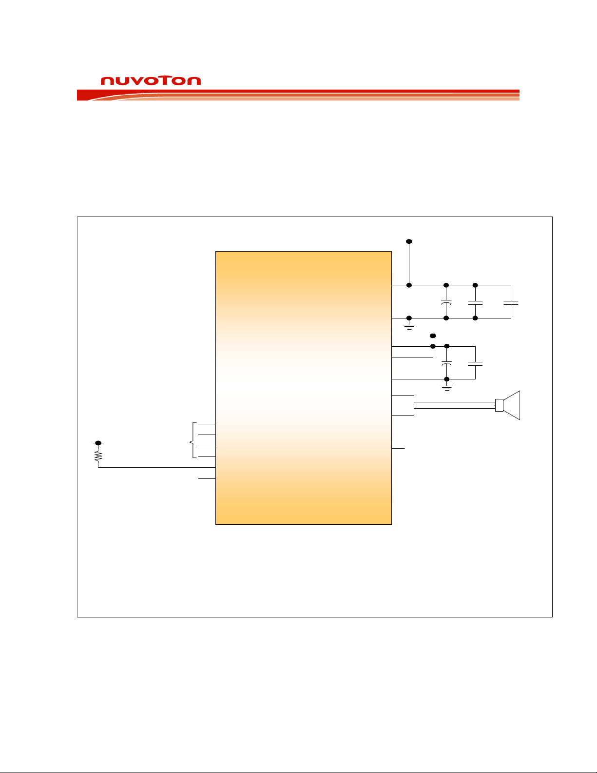
APPLICATION DIAGRAM
10
The following applications example is for references only. It makes no representation or warranty that
such applications shall be suitable for the use specified. Each design has to be optimized in its own
system for the best performance on voice quality, current consumption, functionalities and etc.
Figure 12-1 ISD2100 Application Diagram
The above application examples are for references only. It makes no representation or warranty that such applications shall be
suitable for the use specified. Each design has to be optimized in its own system for the best performance on voice quality,
current consumption, functionalities and etc.
Publication Release Feb 9, 2010
- 15 - Revision 0.51
Page 16
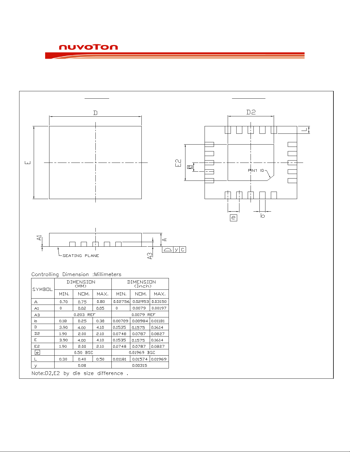
PACKAGE SPECIFICATION
T OP V I E W B OT T O M VI E W
11
6
20
15
10
15
16
16
15 11
10
6
51
20
11
11.1 20 LEAD QFN
ISD2100 DATASHEET
Publication Release Feb 9, 2010
- 16 - Revision 0.51
Page 17
Y: green
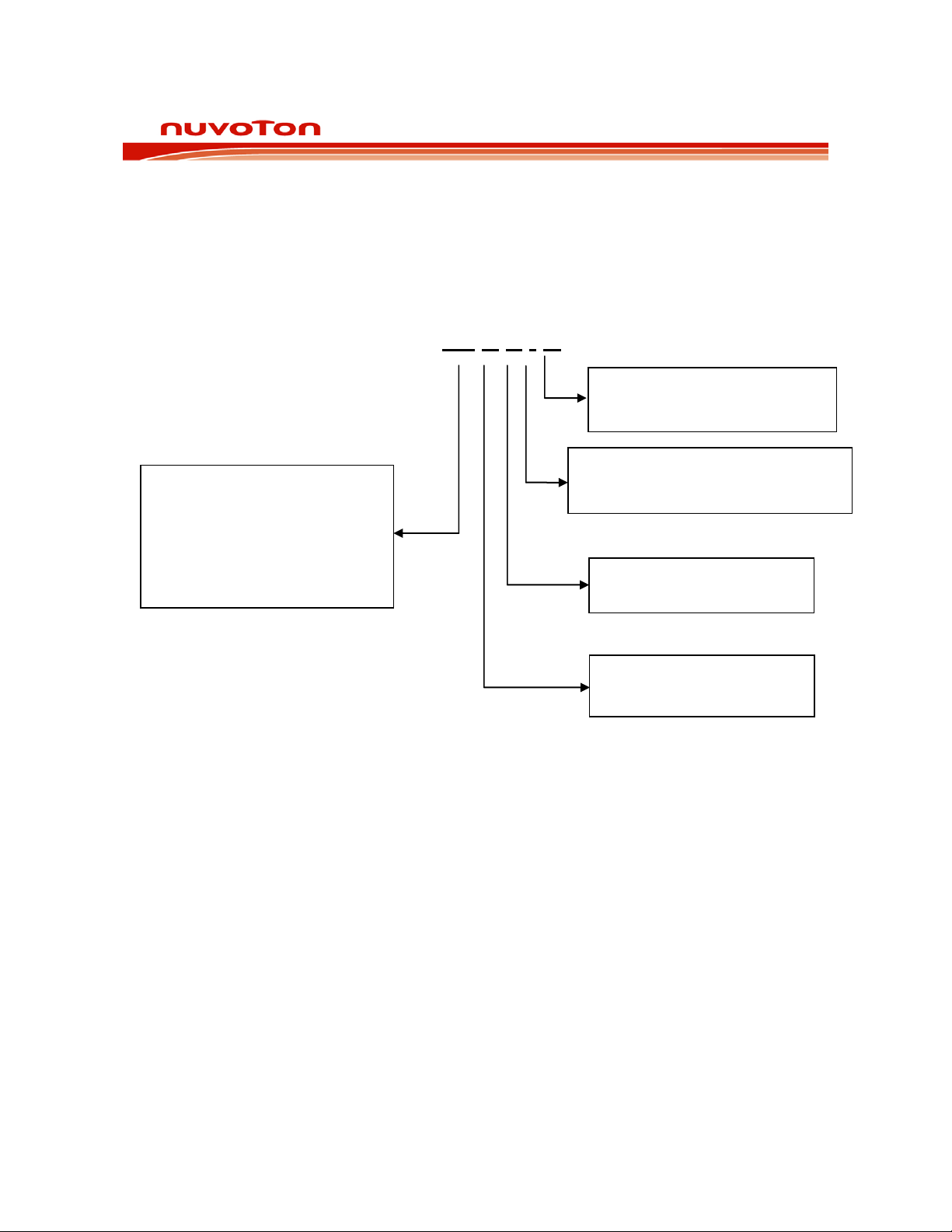
12 ORDERING INFORMATION
ISD2100 DATASHEET
Duration
30: 30 Seconds
* Based on 8kHz/4bit ADPCM
I21XX
X Y I R
R: Tape and Reel
Temperature
I: Industrial -40°C to 85°C
Package Option
Package Type
Y: 20L-QFN
Publication Release Feb 9, 2010
- 17 - Revision 0.51
Page 18

REVISION HISTORY
13
Version Date Description
0.2 Jan 29, 2009 Initial draft.
0.45 August 5, 2009 Add Wake-Up VM description
0.46 November 11, 2009 Add Checksum Description
0.48 January 9, 2010 Simplify all Block diagrams
0.51 Feb 4, 2010 Update description
ISD2100 DATASHEET
Publication Release Feb 9, 2010
- 18 - Revision 0.51
Page 19

ISD2100 DATASHEET
Nuvoton products are not designed, intended, authorized or warranted for use as components in systems or equipment
intended for surgical implantation, atomic energy control instruments, airplane or spaceship instruments, transportation
instruments, traffic signal instruments, combustion control instruments, or for other applications intended to support or
sustain life. Furthermore, Nuvoton products are not intended for applications wherein failure of Nuvoton products could
result or lead to a situation wherein personal injury, death or severe property or environmental damage could occur.
Nuvoton customers using or selling these products for use in such applications do so at their own risk and agree to fully
indemnify Nuvoton for any damages resulting from such improper use or sales.
The contents of this document are provided only as a guide for the applications of Nuvoton products. Nuvoton makes no
representation or warranties with respect to the accuracy or completeness of the contents of this publication and
reserves the right to discontinue or make changes to specifications and product descriptions at any time without notice.
No license, whether express or implied, to any intellectual property or other right of Nuvoton or others is granted by this
publication. Except as set forth in Nuvoton's Standard Terms and Conditions of Sale, Nuvoton assumes no liability
whatsoever and disclaims any express or implied warranty of merchantability, fitness for a particular purpose or
infringement of any Intellectual property.
The contents of this document are provided “AS IS”, and Nuvoton assumes no liability whatsoever and disclaims any
express or implied warranty of merchantability, fitness for a particular purpose or infringement of any Intellectual
property. In no event, shall Nuvoton be liable for any damages whatsoever (including, without limitation, damages for
loss of profits, business interruption, loss of information) arising out of the use of or inability to use the contents of this
documents, even if Nuvoton has been advised of the possibility of such damages.
Application examples and alternative uses of any integrated circuit contained in this publication are for illustration only
and Nuvoton makes no representation or warranty that such applications shall be suitable for the use specified.
The 100-year retention and 100K record cycle projections are based upon accelerated reliability tests, as published in
the Nuvoton Reliability Report, and are neither warranted nor guaranteed by Nuvoton.
This datasheet and any future addendum to this datasheet is(are) the complete and controlling ISD
product specifications. In the event any inconsistencies exist between the information in this and other product
documentation, or in the event that other product documentation contains information in addition to the information in
this, the information contained herein supersedes and governs such other information in its entirety. This datasheet is
subject to change without notice.
Copyright
Nuvoton Electronics Corporation. All other trademarks are properties of their respective owners.
©
2005, Nuvoton Technology Corporation. All rights reserved. ChipCorder® and ISD® are trademarks of
®
ChipCorder®
Headquarters Nuvoton Technology Corporation America Nuvoton Technology (Shanghai) Ltd.
No. 4, Creation Rd. III 2727 North First Street, San Jose, 27F, 299 Yan An W. Rd. Shanghai,
Science-Based Industrial Park, CA 95134, U.S.A. 200336 China
Hsinchu, Taiwan TEL: 1-408-9436666 TEL: 86-21-62365999
TEL: 886-3-5770066 FAX: 1-408-5441797 FAX: 86-21-62356998
FAX: 886-3-5665577 http://www.nuvoton-usa.com/
http://www.nuvoton.com.tw/
Taipei Office Nuvoton Technology Corporation Japan Nuvoton Technology (H.K.) Ltd.
9F, No. 480, Pueiguang Rd. 7F Daini-ueno BLDG. 3-7-18 Unit 9-15, 22F, Millennium City,
Neihu District Shinyokohama Kohokuku, No. 378 Kwun Tong Rd.,
Taipei, 114 Taiwan Yokohama, 222-0033 Kowloon, Hong Kong
TEL: 886-2-81777168 TEL: 81-45-4781881 TEL: 852-27513100
FAX: 886-2-87153579 FAX: 81-45-4781800 FAX: 852-27552064
Please note that all data and specifications are subject to change without notice.
All the trademarks of products and companies mentioned in this datasheet belong to their respective owners.
Publication Release Feb 9, 2010
- 19 - Revision 0.51
 Loading...