

Page 1

ADVANCED
ISD18B12
SINGLE-CHIP, SINGLE-MESSAGE
VOICE RECORD/PLAYBACK DEVICE
6- TO 12-SECONDS DURATION
Publication Release Date: August 17, 2007
- 1 - Revision A1
Page 2

ISD18B12
TABLE OF CONTENTS
1. GENERAL DESCRIPTION ............................................................................................................... 3
2. FEATURES ....................................................................................................................................... 3
3. BLOCK DIAGRAM ........................................................................................................................... 4
4. PAD DESCRIPTION ......................................................................................................................... 5
5. FUNCTIONAL DESCRIPTION ......................................................................................................... 6
6. ABSOLUTE MAXIMUM RATINGS ................................................................................................ 11
6.1 Operating Conditions ................................................................................................................... 11
7. ELECTRICAL CHARACTERISTICS.............................................................................................. 12
7.1. DC Parameters ........................................................................................................................... 12
7.2. AC Parameters ........................................................................................................................... 13
8. TYPICAL APPLICATION CIRCUIT ............................................................................................... 14
9. DIE INFORMATION ........................................................................................................................ 16
10. ORDERING INFORMATION .......................................................................................................... 17
11. VERSION HISTORY ....................................................................................................................... 18
- 2 -
Page 3
ISD18B12
1. GENERAL DESCRIPTION
Winbond’s ISD18B12 ChipCorder® is a new single-chip single-message record/playback device with a
special TryMe feature. The user-selectable duration is from 6 to 12 seconds, with wide operating
voltage ranging from 2.4V to 5.5V. Its sampling frequency, ranging from 4kHz to 8kHz, is externally
controlled via resistor at Rosc pin. This device also includes microphone amplifier, anti-aliasing filter,
multilevel storage array, smoothing filter and speaker amplifier. Two external resistors are used to
adjust the microphone amplifier gain for the incoming signal. Thus, a minimum record/playback
subsystem can be configured with a microphone, a speaker, several passive components, two push
buttons, and a power source.
Recordings are stored into on-chip non-volatile memory, providing zero-power message storage. This
unique, single-chip solution is made possible through Winbond’s patented Multi-Level Storage
technology. Voice and audio signals are stored directly into memory in their natural form, providing
high-quality, solid-state voice reproduction. The device is automatically power down after each
operation cycle with typical standby current, 1µA. With the embedded Flash memory employed, data
retention up to 100 years and typical 100,000 erase/record cycles can be reached.
2. FEATURES
• Supply voltage: 2.4V to 5.5V
• User-selected variable sampling frequency and duration via external resistor
Sampling Frequency 8 kHz 6.4 kHz 5.3 kHz 4 kHz
Rosc 80 KΩ 100 KΩ 120 KΩ 160 KΩ
Duration 6 secs 7.5 secs 9 secs 12 secs
• RECL : Level recording
RECE : Edge-trigger, toggle on-off
•
PLAYE : Edge-trigger, toggle on-off
•
PLAYL
•
•
•
•
: Level playback or looping playback
LEDR : LED output for recording
LEDP : LED output for playback
FT : Feed-through microphone input to speaker outputs
• Microphone amplifier gain: user control via two external resistors
• With feed-through enabled, r
ecord microphone signal into memory while feed-through path
remains active
• Playback takes precedence over the Recording operation
TryMe : TryMe special mode
•
• Package option: die only
• Temperature options: 0°C to +50°C
Publication Release Date: August 31, 2007
- 3 - Revision A1
Page 4
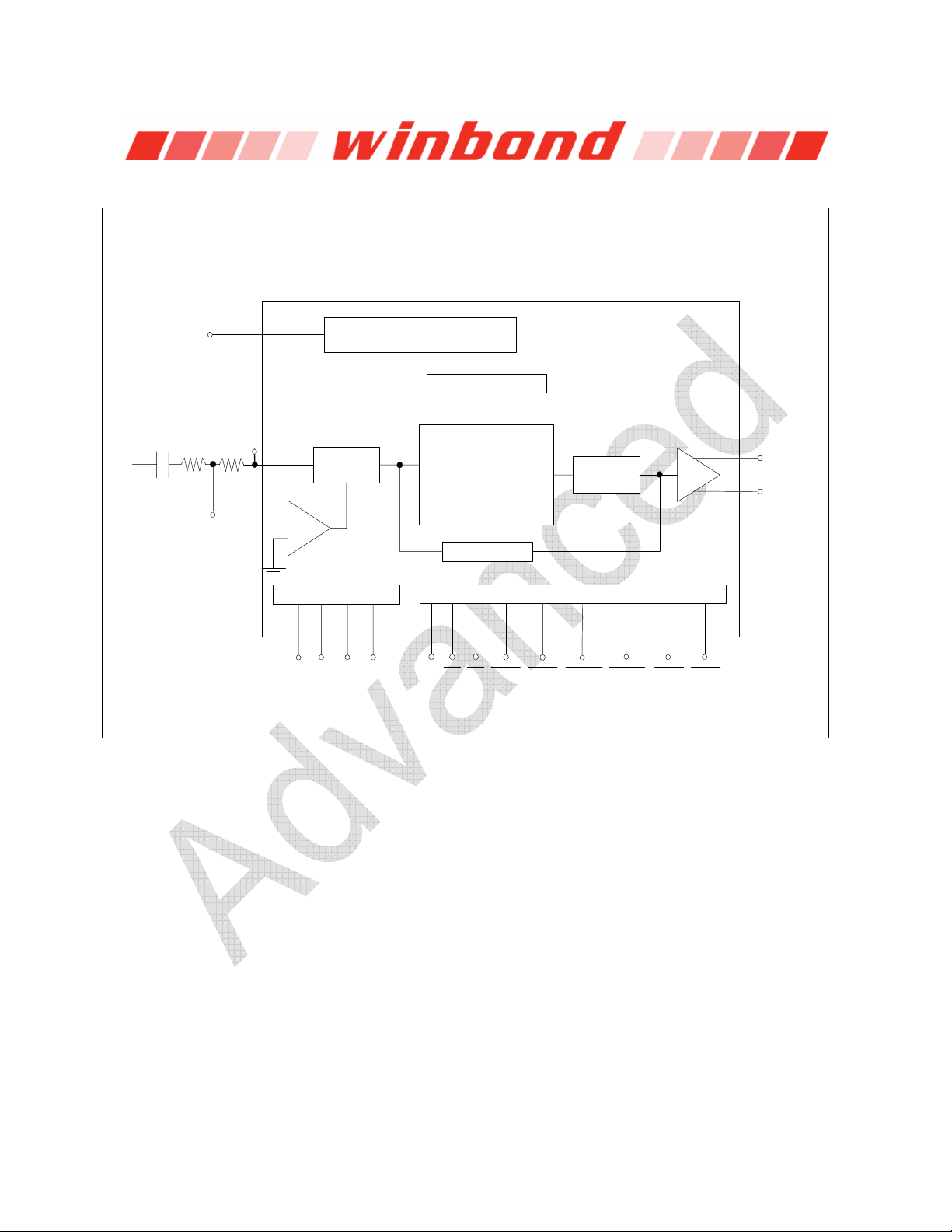
3. BLOCK DIAGRAM
ISD18B12
INPUT
R
OSC
MICIN
MICOUT
R
I
Clock Control
Sampling Clock
Filter
R
O
Amp
Power Conditioning
V
V
SSAVSSDVCCD
CCA
Non-Volatile
Multi Level Storage
Array
Switch
TryMe
SE
RECL LEDPFT
Filter
Device Control
RECE
Amp
LEDRPLAYLPLAYE
SP+
SP-
- 4 -
Page 5
4. PAD DESCRIPTION
PAD NAME I / O FUNCTION
V
I
SSD
RECL
PLAYE
PLAYL
RECE
NC -- NC: No Connect
NC -- NC: No Connect
NC -- NC: No Connect
NC -- NC: No Connect
MICIN I
NC -- NC: No Connect
MICOUT O
NC -- NC: No Connect
NC -- NC: No Connect
SP- O
V
I
SSA
SP+ O
V
I
CCA
Rosc I
FT
NC -- NC: No Connect
NC -- NC: No Connect
TryMe
Digital Ground: Ground path for digital circuits.
I
Level-Triggered Record: Low active input, Level-hold.
I
Edge-Triggered Playback: Low active input, Edge-trigger,
I
Level-Triggered Playback: Low active input, Level-hold.
I
Edge-Triggered Record: Low active input, Edge-trigger,
Microphone Input: The MICIN transfers input signal to the on-chip
microphone amplifier.
Microphone Output: Output of the microphone amplifier.
SP-: The negative signal of the differential speaker outputs.
Analog Ground: Ground path for analog circuits.
SP+: The positive signal of the differential speaker outputs.
Power Supply: Power supply for analog circuits.
Oscillator Resistor: Connect an external resistor from this pin to V
select the sampling frequency
I
Feed-Through (FT): Low active input, Level-hold, Feed-through microphone
input to speaker outputs while in active state.
I
TryMe Mode : High active input, Level-hold. A special operating mode.
ISD18B12
toggle on-off.
toggle on-off.
SSA
to
LED output for Playback: During playback, this output is Low.
LEDP
NC -- NC: No Connect
SE
V
I
CCD
LEDR
O
I
Sound Effect: Low active input, Level-hold, optional beeping sound effect.
Power Supply: Power supply for digital circuits.
LED output for Recording: During recording, this output is Low.
O
Publication Release Date: August 31, 2007
- 5 - Revision A1
Page 6
ISD18B12
5. FUNCTIONAL DESCRIPTION
For the following related operations, if SE is not enabled, then no beep sound is heard. Also, the timing diagrams
may not be in direct proportional scale.
5.1. Level-triggered Record (
• Recording starts from beginning of the memory and
• Recording ceases whenever
RECL
) Operation :
RECL
LEDR is on.
returns to High or when end of memory is reached and
off.
• Then device will automatically power down.
Fig. 1: Record–Level (
T
r
RECL
LEDR
BEEP
(Optional)
MicIn
LEDP
5.2. Edge-triggered Record (
• Recording starts from beginning of the memory and
RECL ) function till memory full
T
Deb
T
B1
T
D1
RECE
)Operation :
Memory Full
LEDR is on.
• Recording ceases whenever a subsequent trigger occurs at
LEDR is off.
and
• Then device will automatically power down.
T
f
T
B2
T
P2
RECE
or when end of memory is reached
LEDR
is
Fig. 2: Record–Edge (
T
r
RECL
T
LEDR
BEEP
(Optional)
MicIn
LEDP
RECE ) function with on-off
T
f
T
Deb
T
B1
T
D1
Deb
T
B2
Stop
T
Deb
T
B1
T
D1
T
P2
Memory Full
T
B2
T
P2
- 6 -
Page 7

ISD18B12
5.3. Edge-triggered playback (
• Playback starts from beginning of the memory and
PLAYE ) Operation :
LEDP is on.
• Playback stops whenever end of message or a subsequent trigger occurs and
• Then device will automatically power down.
Fig. 3 : Playback–Edge (
T
r
PlayE
Start Stop
LEDP
SP+
SP-
LEDR
5.4. Level- triggered playback (
• Playback starts from beginning of the memory and
• Playback stops whenever an EOM marker is reached or
PLAYE ) function
T
f
T
Deb
T
PLAYL
Deb
T
P1
)Operation :
Start
T
Deb
End of Message
LEDP is on.
PLAYL
returns to High and
• Then device will automatically power down.
LEDP is off.
T
P1
LEDP
is off.
Fig. 4: Playback–Level (
T
r
PLAYL ) function
T
f
PlayL
T
Deb
T
Deb
LEDP
End of Message
SP+
SP-
T
P1
T
P1
LEDR
• Holding
Fig. 5: Looping playback function via
PLAYL Low constantly will perform looping playback function.
PLAYL
Publication Release Date: August 31, 2007
- 7 - Revision A1
Page 8

PlayL
LEDP
ISD18B12
T
r
T
Deb
T
D2
SP+
SP-
LEDR
T
D2
5.5. Sound Effect (
SE ) Operation :
• Beeping feature for recording. Once active, one-beep indicates the start of recording and two-beep
represents the end of recording.
5.6. Microphone amplifier gain
• Two external resistors, RI and RO, are used to adjust the microphone amplifier gain with respect to the
incoming signal.
5.7. Playback (supersedes Record) Operation :
• Playback takes precedence over the Recording operation.
• If either PLAYE or PLAYL is activated during a recording cycle, the recording immediately ceases and
playback of the just-recorded message performs accordingly.
5.8. Feed-Through mode Operation :
• As
• If either
FT is held Low, the input signal from MICIN will directly transmit to the speaker outputs.
RECE is triggered or RECL is held Low simultaneously after FT is enabled, then input signal
will be recorded into memory while the Feed-Through mode is still on.
• After
FT is enabled, activating either PLAYE or PLAYL will first disable the feed-through path and
play the recorded message. Once playback is completed, the feed-through feature resumes.
5.9.
LEDR Operation :
LEDR stays on during recording.
•
• Also,
5.10.
•
• Also,
LEDR pulses Low momentarily at the end of playback operation.
LEDP Operation :
LEDP stays on during playback.
LEDP pulses Low momentarily at the end of recording.
5.11. Rosc Operation :
• When the R
• When R
varies from 80 KΩ to 160 KΩ, the duration changes from 6 to 12 seconds accordingly.
OSC
resistor value is changed during playback, the tone of a recorded message will alter either
OSC
faster or slower.
5.12. Speaker Outputs
• Both SP+ and SP- outputs can be used to drive an 8Ω speaker differentially. They are tri-state while
device is in power down status.
- 8 -
Page 9

ISD18B12
5.13. TryMe Special Operation :
This is a special feature. When
The enabling and disabling of this feature is merely permitted while the device is in power down status. Once
TryMe is set, trigger on either RECL or RECE will initiate the TryMe operation sequence. While active, the
device performs a combination of the following 3 operations sequentially: Record a new message and
automatic playback the just-recorded message once, then delete the recorded message. Internal pull-up
exists.
The details of each operation are described as follows:
a) Recording:
• The recording behavior follows the characteristics of the selected record pin,
• While recording, the
b) Playback:
• Upon completion of recording, the device automatic plays the just-recorded message once and
stops. During this operation, change of state on any control pins is prohibited.
• While playback, the LEDP is on if an LED is connected appropriately.
c) Erasure:
• Upon completion of playback, the device will involuntary delete the recorded message. During this
operation, change of state on any control pins is banned.
After completion of this TryMe operation, the device returns to standby state automatically. Once playback
operation starts, any input on other controls is illegal.
TryMe is High, TryMe is active. When TryMe is Low, TryMe is disabled.
RECL or RECE .
LEDR is on if an LED is connected appropriately.
As a summary, the TryMe mode starts in the following conditions:
Pin
Logic Level 1 0 1
Under no circumstances, while this special operation is in progress, neither the power is disturbed
nor any change of state on other control pins are permitted. Otherwise, it may cause the device
becoming malfunction.
Fig 6: TryMe function via (
TryMe
1 1 0
RECL RECE
TryMe + RECL )
Publication Release Date: August 31, 2007
- 9 - Revision A1
Page 10

ISD18B12
TM
RECL
LEDR
BEEP
(Optional)
MicIn
LEDP
PLAYE
or PLAYL
SP+
SP-
T
r
Illegal state
T
Deb
T
B2
T
B1
T
D1
Illegal state
T
P1
T
f
5.14. Power interruption
• Any power interruption during an operation is strongly not recommended. If happened, it may result the
device becoming malfunction.
5.15. Power-On to Playback Operation :
PLAYE or PLAYL is held at Low during power turns on, the device plays message accordingly with
• If
respect to which play control being employed.
5.16. Power-On to Loop Playback Operation :
• If
PLAYL is hardwired to ground permanently, once power is on, the device performs looping playback
non-stop. This status will sustain unless power is turned off.
5.17. Automatic Playback after Record Operation :
• If
LEDP
is connected to
PLAYE
, after a record operation, then the device will automatic play message
once, then powers down.
- 10 -
Page 11

ISD18B12
6. ABSOLUTE MAXIMUM RATINGS
ABSOLUTE MAXIMUM RATINGS
CONDITION VALUE
Junction temperature 150°C
Storage temperature range -65°C to +150°C
Voltage applied to any pins (VSS – 0.3V) to (VCC + 0.3V)
Voltage applied to Input pins (current limited to +/-20 mA) (VSS – 1.0V) to (VCC + 1.0V)
Voltage applied to output pins (current limited to +/-20 mA) (VSS – 1.0V) to (VCC + 1.0V)
VCC – VSS -0.3V to +7.0V
[1]
Stresses above those listed may cause permanent damage to the device. Exposure
to the absolute maximum ratings may affect device reliability and performance.
Functional operation is not implied at these conditions.
[1]
6.1 OPERATING CONDITIONS
Operating temperature range 0°C to +50°C
Operating voltage (VCC)
Ground voltage (VSS)
[1]
VCC = V
[2]
VSS = V
CCA
SSA
= V
= V
CCD
SSD
OPERATING CONDITIONS
CONDITION VALUE
[1]
+2.4V to +5.5V
[2]
0V
Publication Release Date: August 31, 2007
- 11 - Revision A1
Page 12

7. ELECTRICAL CHARACTERISTICS
7.1. DC PARAMETERS
ISD18B12
PARAMETER SYMBOL MIN
[2]
TYP
[1]
MAX
[2]
UNITS CONDITIONS
Input Low Voltage VIL 0.3xVcc V
Input High Voltage VIH 0.7xVcc V
Output Low Voltage VOL 0.3xVcc V I
Output High Voltage VOH 0.7xVcc V I
Standby Current I
Record Current I
Playback Current I
1 10 µA
STBY
15 mA V
REC
15 mA V
PLAY
= 4.0 mA
OL
= -1.6 mA
OH
[4] [5]
= 5.5V
CC
= 5.5V, no
CC
[3]
[3]
speaker load
Pull-up device for
RECE, PLAYE, PLAYL, FT
TryMe pins
&
RECL
,
Pull-up device for SE
Output Load Impedance R
40
PU1
R
80
PU2
8 Ω Speaker load
EXT
kΩ
kΩ
R
MIC Input Voltage VIN 4 400 mV Peak-to-peak
MIC Amplifier Gain A
0 +34 dB Depend on
MicAmp
RO/RI
Gain from MIC to SP+/SP- A
+12 +46 dB Depend on
MSP
RO/RI
Notes:
[1]
Typical values @ TA = 25°, VCC = 5.5V and sampling frequency (Fs) at 8 kHz, unless stated.
[2]
All Min/Max limits are guaranteed by design, electrical testing and/or characterization. Not all
specifications are 100 percent tested.
[3]
LED output during recording.
[4]
V
and V
CCA
[5]
RECL , RECE , PLAYE , PLAYL , SE , FT and TryMe must be at V
biased under a separated power supply.
are connected together. Also, V
CCD
SSA
and V
are connected together.
SSD
. External components are
CCD
- 12 -
Page 13

7.2. AC PARAMETERS
ISD18B12
CHARACTERISTIC SYMBOL MIN
Sampling Frequency
Record Duration
Playback Duration
Rising Time
Falling Time
Debounce Time
Beep Duration
Beep-Beep Duration
Delay to start recording
Delay during looping
LEDR Pulse Low Time
LEDP Pulse Low Time
FS
T
REC
T
PLAY
Tr
Tf
T
Deb
TB1
TB2
TD1
TD2
TP1
TP2
[2]
TYP
4
6 12 sec Depend on Fs
6 12 sec Depend on Fs
100 nsec
100 nsec
536k/FS msec
512k/FS msec
1536k/FS msec
1552k/FS msec
1k/FS msec
1024k/FS msec
1280k/FS msec
[1]
MAX
[2]
UNITS CONDITIONS
8 kHz
[3]
[3]
[3]
[3] [4]
[3] [4]
[3] [4]
[3] [4]
[3] [4]
[3] [4]
[3] [4]
Notes:
[1]
Conditions are VCC = 5.5V and TA = 25°C, unless specified.
[2]
All Min/Max limits are guaranteed by design, electrical testing and/or characterization. Not all
specifications are 100 percent tested.
[3]
The value changes accordingly to the FS applied. Also, the internal oscillator may vary as much as +10%
over the operating temperature and voltage ranges.
[4]
k=1000
[3]
[3]
Publication Release Date: August 31, 2007
- 13 - Revision A1
Page 14

ISD18B12
8. TYPICAL APPLICATION CIRCUIT
The following typical application examples on ISD18B12 series are for references only. They make
no representation or warranty that such applications shall be suitable for the use specified. Each
design has to be optimized in its own system for the best performance on voice quality, current
consumption, functionalities and etc. It’s customer’s obligation to confirm the design on all the
functionalities of their end-products.
In addition, the below notes apply to the following application examples:
* The suggested values are for references only. Depending on system requirements, they must
be fine tuned for best performance.
It is important to have a separate path for each ground and power back to the related terminals to
minimize the noise. Besides, the power supplies should be decoupled as close to the device as
possible.
Also, it is crucial to follow good audio design practices in layout and power supply decoupling. See
recommendations in Application Notes from our websites.
Example #1: Typical Recording and Playback operations
V
CCD
V
SSD
V
CCA
V
SSA
SP-
SP+
MICOUT
MICIN
FT
SE
0.1 F
500k
Beeping
(Optional)
µ
Ω∗
0.1 F
µ
10k
Ω∗
Speaker
µ
0.1 F*
10k
10 F*
Vcc
Ω∗
µ
1k
Ω∗
µ
10 F*
ELECTRET
MICROPHONE
LEDR
PLAYL
PLAYE
RECE
RECL
80 K
1 K
Ω
LEDR
1 K
Ω
LEDP
PLAYL
PLAYE
I18B12
Or
Ω∗
RECE
TryMe
RECL
R
OSC
- 14 -
Page 15

Example #2: TryMe feature
ISD18B12
V
CCD
V
SSD
V
CCA
V
SSA
SP-
SP+
MICOUT
MICIN
TryMe
SE
0.1 F
500kΩ∗
Vcc
Beeping
(Optional)
µ
0.1 F
µ
10k
Ω∗
Speaker
µ
0.1 F*
10kΩ∗
µ
10 F*
Vcc
1k
Ω∗
10 F*
ELECTRET
MICROPHONE
µ
LEDR
RECE
RECL
80 K
1 K
1 K
Ω∗
Ω
LEDR
Ω
LEDP
PLAYL
PLAYE
I18B12
RECE
RECL
FT
R
OSC
Good Audio Design Practices
Winbond’s ChipCorder are very high-quality single-chip voice recording and playback devices.
To ensure the highest quality voice reproduction, it is important that good audio design
practices on layout and power supply decoupling are followed. See Application Information
links below for details.
Good Audio Design Practices
http://www.winbond-usa.com/products/isd_products/chipcorder/applicationinfo/apin11.pdf
Single-Chip Board Layout Diagrams
http://www.winbond-usa.com/products/isd_products/chipcorder/applicationinfo/apin12.pdf
It is strongly recommended that before any design or layout project starts, the designer should contact
Winbond Sales Rep for the most update technical information.
Publication Release Date: August 31, 2007
- 15 - Revision A1
Page 16

9. DIE INFORMATION
ISD18B12
PLAYL PLAYE RECL
RECE
V
SSD
LEDR
ISD18B12
V
CCD
SE
LEDP
TryMe
FT
MICIN MICOUT SP- V
Contact Winbond Sales Representatives for information.
SSA
SP + V
- 16 -
CCA
Rosc
Page 17

ISD18B12
10. ORDERING INFORMATION
Product Number Descriptor Key
When ordering, please refer to the following part numbers that are supported in volume for this
product series. Consult the local Winbond Sales Representative or Distributor for availability
information.
ISD18B Series
Duration:
12 = 6- to 12-second
ISD18Bxxxx
Temperature:
Blank = Commercial
• Die (0°C to +50°C)
Package Type:
X = Die
Package Part Number Ordering Number Comments
Die
For the latest product information, access Winbond’s worldwide website at
http://www.winbond-usa.com
- 17 - Revision A1
ISD18B12X I18B12X
Publication Release Date: August 31, 2007
Page 18

11. VERSION HISTORY
VERSION DATE DESCRIPTION
A0 May 2007 Pre-released version
A1 August 2007 Initial revision
ISD18B12
- 18 -
Page 19
ISD18B12
prop
Winbond products are not designed, intended, authorized or warranted for use as components in systems or equipment
intended for surgical implantation, atomic energy control instruments, airplane or spaceship instruments, transportation
instruments, traffic signal instruments, combustion control instruments, or for other applications intended to support or
sustain life. Furthermore, Winbond products are not intended for applications wherein failure of Winbond products could
result or lead to a situation wherein personal injury, death or severe property or environmental damage could occur.
Winbond customers using or selling these products for use in such applications do so at their own risk and agree to fully
indemnify Winbond for any damages resulting from such improper use or sales.
The contents of this document are provided only as a guide for the applications of Winbond products. Winbond makes no
representation or warranties with respect to the accuracy or completeness of the contents of this publication and
reserves the right to discontinue or make changes to specifications and product descriptions at any time without notice.
No license, whether express or implied, to any intellectual property or other right of Winbond or others is granted by this
publication. Except as set forth in Winbond's Standard Terms and Conditions of Sale, Winbond assumes no liability
whatsoever and disclaims any express or implied warranty of merchantability, fitness for a particular purpose or
infringement of any Intellectual property.
The contents of this document are provided “AS IS”, and Winbond assumes no liability whatsoever and disclaims any
express or implied warranty of merchantability, fitness for a particular purpose or infringement of any Intellectual
property. In no event, shall Winbond be liable for any damages whatsoever (including, without limitation, damages for
loss of profits, business interruption, loss of information) arising out of the use of or inability to use the contents of this
documents, even if Winbond has been advised of the possibility of such damages.
Application examples and alternative uses of any integrated circuit contained in this publication are for illustration only
and Winbond makes no representation or warranty that such applications shall be suitable for the use specified.
The 100-year retention and 100K record cycle projections are based upon accelerated reliability tests, as published in
the Winbond Reliability Report, and are neither warranted nor guaranteed by Winbond. This product incorporates
SuperFlash
Information contained in this ISD
published by ISD
This datasheet and any future addendum to this datasheet is(are) the complete and controlling ISD
product specifications. In the event any inconsistencies exist between the information in this and other product
documentation, or in the event that other product documentation contains information in addition to the information in
this, the information contained herein supersedes and governs such other information in its entirety. This datasheet is
subject to change without notice.
Copyright
Winbond Electronics Corporation. SuperFlash
are
®
.
®
®
prior to August, 1998.
©
2005, Winbond Electronics Corporation. All rights reserved. ChipCorder® and ISD® are trademarks of
erties of their respective owners.
ChipCorder® datasheet supersedes all data for the ISD ChipCorder products
®
ChipCorder®
®
is the trademark of Silicon Storage Technology, Inc. All other trademarks
Please note that all data and specifications are subject to change without notice.
All the trademarks of products and companies mentioned in this datasheet belong to their respective owners.
Publication Release Date: August 31, 2007
- 19 - Revision A1
 Loading...