

Page 1

PRELIMINARY
ISD1700
Series
Multi-Message
Single-Chip
Voice Record & Playback Devices
Publication Release Date: January 23, 2007
Revision 1.3-S2
Page 2

ISD1700 SERIES
TABLE OF CONTENTS
1 GENERAL DESCRIPTION ..............................................................................................................3
2 FEATURES......................................................................................................................................4
3 BLOCK DIAGRAM...........................................................................................................................5
4 PINOUT CONFIGURATION............................................................................................................6
5 PIN DESCRIPTION .........................................................................................................................7
6 MODES OF OPERATIONS.............................................................................................................8
6.1 Standalone (Push-Button) Mode .............................................................................................8
6.2 SPI Mode .................................................................................................................................8
7 TIMING DIAGRAMS ........................................................................................................................8
7.1 Standalone Operation ..............................................................................................................8
7.2 SPI Operation.........................................................................................................................12
8 ABSOLUTE MAXIMUM RATINGS ................................................................................................13
8.1 Operating Conditions .............................................................................................................13
9 ELECTRICAL CHARACTERISTICS .............................................................................................14
9.1 DC Parameters ......................................................................................................................14
9.2 AC Parameters.......................................................................................................................15
10 TYPICAL APPLICATION CIRCUITS.............................................................................................16
10.1 Good Audio Design Practices................................................................................................18
11 PACKAGING .................................................................................................................................19
11.1 28-Lead 8x13.4mm Plastic Thin Small Outline Package (TSOP) Type 1 - IQC....................19
11.2 28-Lead 300-Mil Plastic Small Outline Integrated Circuit (SOIC)..........................................20
11.3 28-Lead 600-Mil Plastic Dual Inline Package (PDIP) ............................................................21
11.4 Die Information.......................................................................................................................21
12 ORDERING INFORMATION .........................................................................................................22
13 VERSION HISTORY......................................................................................................................23
- 2 -
Page 3

ISD1700 SERIES
1 GENERAL DESCRIPTION
The Winbond® ISD1700 ChipCorder® Series is a high quality, fully integrated, single-chip multimessage voice record and playback device ideally suited to a variety of electronic systems. The
message duration is user selectable in ranges from 26 seconds to 120 seconds, depending on the
specific device. The sampling frequency of each device can also be adjusted from 4 kHz to 12 kHz
with an external resistor, giving the user greater flexibility in duration versus recording quality for each
application. Operating voltage spans a range from 2.4 V to 5.5 V to ensure that the ISD1700 devices
are optimized for a wide range of battery or line-powered applications.
The ISD1700 is designed for operation in either standalone or microcontroller (SPI) mode. The device
incorporates a proprietary message management system that allows the chip to self-manage address
locations for multiple messages. This unique feature provides sophisticated messaging flexibility in a
simple push-button environment. The devices include an on-chip oscillator (with external resistor
control), microphone preamplifier with Automatic Gain Control (AGC), an auxiliary analog input, antialiasing filter, Multi-Level Storage (MLS) array, smoothing filter, volume control, Pulse Width
Modulation (PWM) Class D speaker driver, and current/voltage output.
The ISD1700 devices also support an optional “vAlert” (voiceAlert) feature that can be used as a new
message indicator. With vAlert, the device flashes an external LED to indicate that a new message is
present. Besides, four special sound effects are reserved for audio confirmation of operations, such as
“Start Record”, “Stop Record”, “Erase”, “Forward”, “Global Erase”, and etc.
Recordings are stored into on-chip Flash memory, providing zero-power message storage. This unique
single-chip solution is made possible through Winbond’s patented Multi-Level Storage (MLS)
technology. Audio data are stored directly in solid-state memory without digital compression, providing
superior quality voice and music reproduction.
Voice signals can be fed into the chip through two independent paths: a differential microphone input
and a single-ended analog input. For outputs, the ISD1700 provides a Pulse Width Modulation (PWM)
Class D speaker driver and a separate analog output simultaneously. The PWM can directly drive a
standard 8Ω speaker or typical buzzer, while the separate analog output can be configured as a
single-ended current or voltage output to drive an external amplifier.
While in Standalone mode, the ISD1700 devices automatically enter into power down mode for power
conservation after an operation is completed.
In the SPI mode, the user has full control via the serial interface in operating the device. This includes
random access to any location inside the memory array by specifying the start address and end
address of operations. SPI mode also allows access to the Analog Path Configuration (APC) register.
This register allows flexible configuration of audio paths, inputs, outputs and mixing. The APC default
configuration for standalone mode can also be modified by storing the APC data into a non-volatile
register (NVCFG) that is loaded at initialization. Utilizing the capabilities of ISD1700 Series, designers
have the control and flexibility to implement voice functionality into the high-end products.
Notice: The specifications are subject to change without notice. Please contact Winbond Sales Offices or
Representatives to verify current or future specifications. Also refer to the website for any related application notes.
Publication Release Date: January 23, 2007
- 3 - Revision 1.3-S2
Page 4
ISD1700 SERIES
Y
2 FEATURES
y Integrated message management systems for single-chip, push-button applications
o
REC : level-trigger for recording
o
o
o
o
o
o
o Automatic power-down after each operation cycle
y Selectable sampling frequency controlled by an external oscillator resistor
duration
o A wide range selection from 20 secs to 480 secs pending upon sampling frequency chosen
Sample Freq. ISD1730 ISD1740 ISD1750 ISD1760 ISD1790 ISD17120 ISD17150 ISD17180 ISD17210 ISD17240
y Message and operation indicators
o Four customizable Sound Effects (SEs) for audible indication
o Optional vAlert (voiceAlert) to indicate the presence of new messages
o LED: stay on during recording, blink during playback, forward and erase operations
y Dual operating modes
o Standalone mode:
o SPI mode:
y Two individual input channels
o MIC+/MIC-: differential microphone inputs with AGC (Automatic Gain Control)
o AnaIn: single-ended auxiliary analog input for recording or feed-through
y Dual output channels
o Differential PWM Class D speaker outputs directly drives an 8 speaker or a typical buzzer
o Configurable AUD (current) or AUX (voltage) single-ended output drives external audio amplifier
y ChipCorder standard features
o High-quality, natural voice and audio reproduction
o 2.4V to 5.5V operating voltage
o 100-year message retention (typical)
o 100,000 record cycles (typical)
: edge-trigger for individual message or level-trigger for looping playback sequentially
PLA
ERASE
FWD
VOL : 8 levels output volume control
RESET : return to the default state
Sampling Frequency 12 kHz 8 kHz 6.4 kHz 5.3 kHz 4 kHz
Rosc
: edge-triggered erase for first or last message or level-triggered erase for all messages
: edge-trigger to advance to the next message or fast message scan during the playback
: ready or busy status indication
INTRDY
y
53 kΩ 80 kΩ 100 kΩ 120 kΩ 160 kΩ
Selectable
message
12 kHz
8 kHz
6.4 kHz
5.3 kHz
4 kHz
20 secs
30 secs
37 secs
45 secs
60 secs
26 secs 33 secs 40 secs 60 secs 80 secs 100 secs 120 secs 140 secs 160 secs
40 secs 50 secs 60 secs 90 secs 120 secs 150 secs 180 secs 210 secs 240 secs
50 secs 62 secs 75 secs 112 secs 150 secs 187 secs 225 secs 262 secs 300 secs
60 secs 75 secs 90 secs 135 secs 181 secs 226 secs 271 secs 317 secs 362 secs
80 secs 100 secs 120 secs 180 secs 240 secs 300 secs 360 secs 420 secs 480 secs
Integrated message management techniques
Automatic power-down after each operation cycle
Fully user selectable and controllable options via APC register and various SPI commands
- 4 -
Page 5
y Temperature options:
o Commercial: 0°C to +50°C (die); 0°C to +70°C (packaged units)
o Industrial: -40°C to +85°C (packaged units)
y Packaging types: available in die, PDIP, SOIC and TSOP
y Package option: Lead-free packaged units
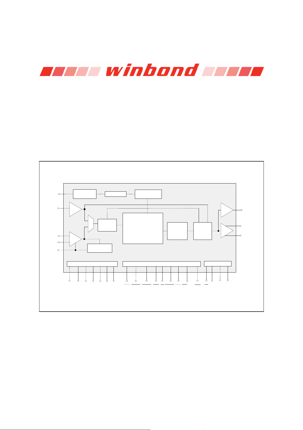
3 BLOCK DIAGRAM
ISD1700 SERIES
R
OSC
AnaIn
MIC+
MIC-
AGC
Internal
Clock
AnaIn
Amp
AGC
Amp
Power Conditioning
V
V
V
SSA
CCA
MUX
Automatic
Gain Control
V
SSP1
CCP
Aliasing
V
SSP2
Anti-
Filter
V
SSD
Timing
V
CCD
Sampling
Clock
Nonvolatile
Multi-Level Storage
Array
Device Control
FWD VOL LEDINT/RDYRESET
FT
Smoothing
Filter
Volume
Control
Amp
Amp
SPI Interface
AUD /
AUX
SP+
SP-
MISOMOSISCLKSSREC PLAY ERASE
Publication Release Date: January 23, 2007
- 5 - Revision 1.3-S2
Page 6
ISD1700 SERIES
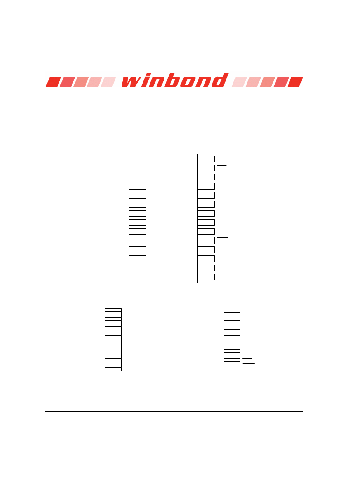
4 PINOUT CONFIGURATION
Refer to Design Guide for details before performing any design or PCB layout.
V
AnaIn
MIC+
MIC-
V
SSP2
SP-
V
CCP
Sp+
V
AUD/AUX
AGC
VOL
R
V
SSA
SSP1
OSC
CCA
V
CCD
LED
RESET
MISO
MOSI
SCLK
SS
V
SSA
AnaIn
MIC+
MIC-
V
SSP2
SP-
V
CCP
ISD1700
SOIC / PDIP
ISD 1 7 0 0
V
SSD
INT / RD Y
FWD
ERASE
REC
PLAY
FT
V
CCA
R
OSC
VOL
AGC
AUD / AUX
V
SSP1
Sp+
SS
SCLK
MOSI
MISO
RESET
LED
V
CCD
V
SSD
INT / RDY
FWD
ERASE
REC
PLAY
FT
TSOP
- 6 -
Page 7
ISD1700 SERIES
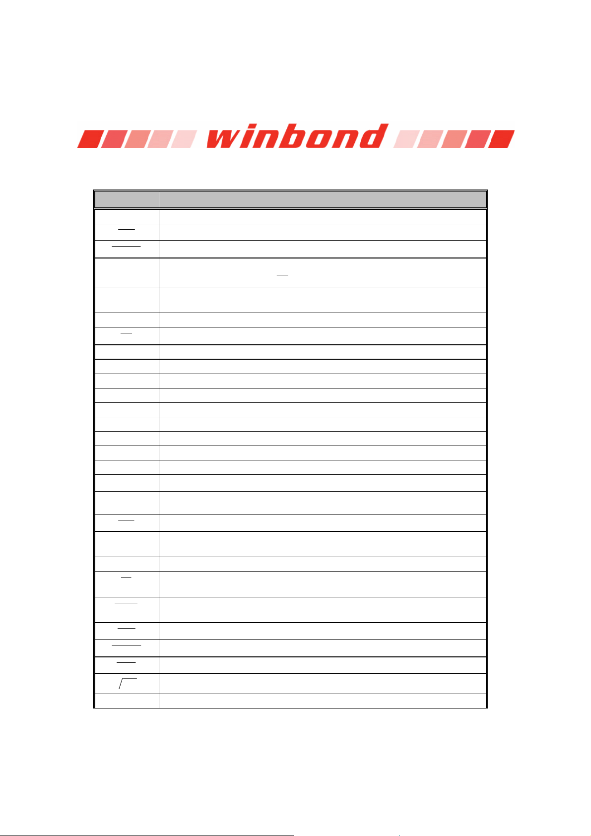
5 PIN DESCRIPTION
Refer to Design Guide for details before performing any design or PCB layout.
PIN NAME FUNCTIONS
V
CCD
LED
RESET
MISO
MOSI
SCLK
SS
V
SSA
AnaIn
MIC+
MIC-
V
SSP2
SP-
V
CCP
SP+
V
SSP1
AUD/AUX
AGC
VOL
R
OSC
V
CCA
FT
PLAY
REC
ERASE
FWD
INTRDY
Digital Power Supply: Power supply for digital circuitry.
LED: An LED output.
RESET: When active, the device enters into a known state.
Master In Slave Out: Data is shifted out on the falling edge of SCLK.
When the SPI is inactive (
SS = high), it’s tri-state.
Master Out Slave In: Data input of the SPI interface when ISD1700 is a
slave. Data is latched into the device on the rising edge of SCLK.
Serial Clock: Clock of the SPI interface.
Slave Select: Selects as a slave device and enables the SPI interface.
Analog Ground: Ground path for analog circuitry.
AnaIn: Auxiliary analog input to the device for recording or feed-through.
MIC+: Non-inverting input of the differential microphone signal.
MIC-: Inverting input of the differential microphone signal.
Ground: Ground path for negative PWM speaker drive.
SP-: The negative Class D PWM speaker output.
Power Supply for PWM Speaker Driver: Power for PWM speaker drive.
SP+: The positive Class D PWM speaker output.
Ground: Ground path for positive PWM speaker drive.
Auxiliary Output: Either an AUD (current) or AUX (voltage) output.
Automatic Gain Control (AGC): The AGC adjusts the gain of the
microphone preamplifier circuitry.
Volume: This control has 8 levels of volume adjustment.
Oscillator Resistor: A resistor determines the sample frequency of the
device, which sets the duration.
Analog Power Supply. Power supply for analog circuitry.
Feed-through: Enable the feed-through path for AnaIn signal to the
outputs.
Playback: Plays the recorded message individually, or plays messages
sequential in a looping mode.
Record: When active, starts recording message.
Erase: When active, can erase individual message or do global erase.
Forward: Advances to the next message from the current location.
An open drain output. Can review ready or interrupt status.
V
SSD
Digital Ground: Ground path for digital circuitry
Publication Release Date: January 23, 2007
- 7 - Revision 1.3-S2
Page 8
ISD1700 SERIES
Y
6 MODES OF OPERATIONS
The ISD1700 Series can operate in either Standalone (Push-Button) or microcontroller (SPI) mode.
6.1 STANDALONE (PUSH-BUTTON) MODE
One can utilize the
REC, PLA
, FT,
FWD
,
ERASE
,
VOL
or
RESET
control to initiate a
desired operation. As completed, the device automatically enters into the power-down state.
6.2 SPI MODE
In SPI mode, control of the device is achieved through the 4-wire serial interface via SPI
commands.
For technical details, please refer to the design guide.
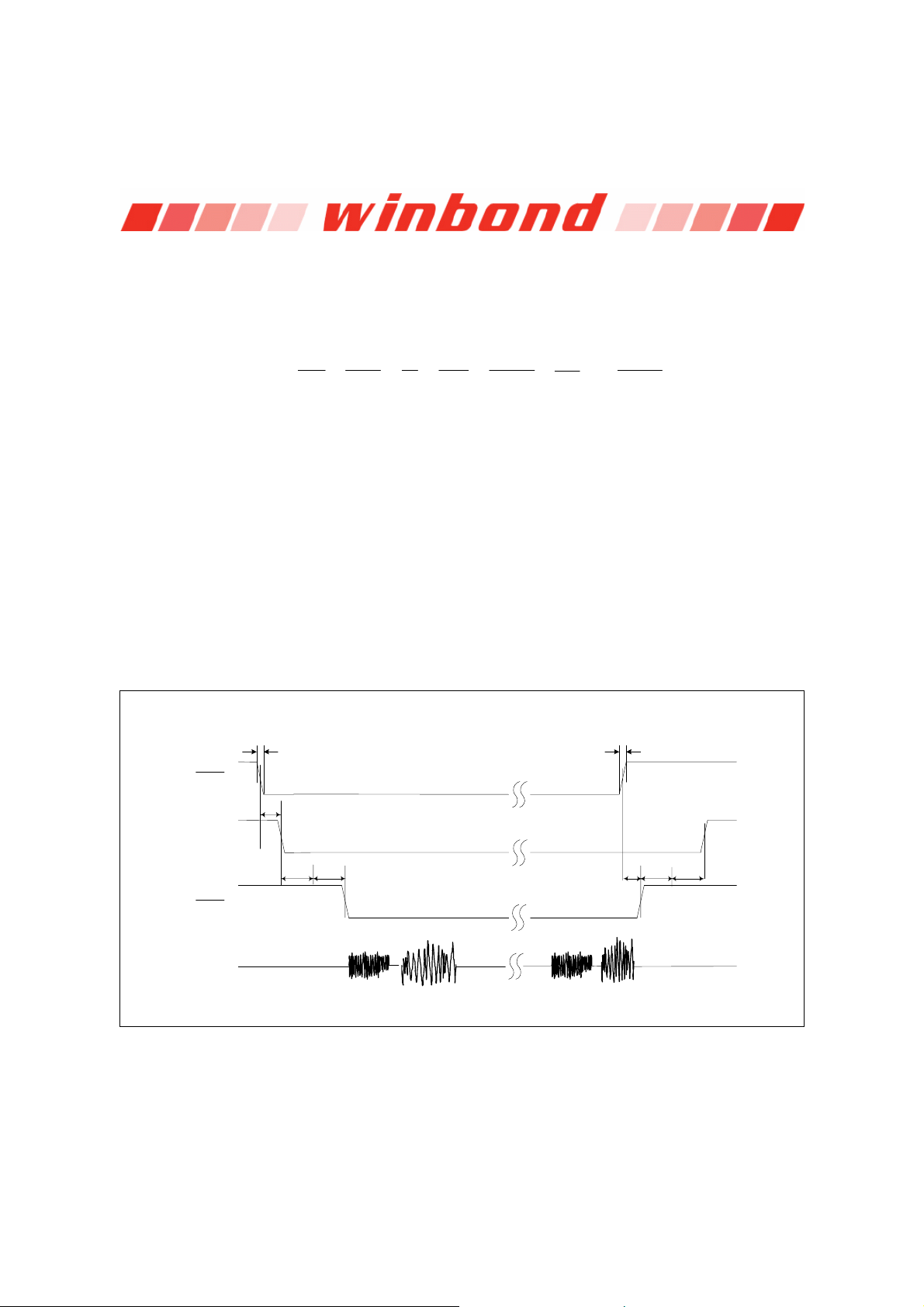
7 TIMING DIAGRAMS
The following estimated timing diagrams are not in proper scale.
ASIC OPERATION
7.1 B
REC
RDY
T
r
T
Deb
T
f
LED
Mic+/-,
AnaIn
T
T
Sc1
RU
T
ER
T
T
Set1
RD
Figure 12.1: Record Operation with No Sound Effect
- 8 -
Page 9

ISD1700 SERIES
T
> T
r
Deb
T
f
PLAY
T
Deb
RDY
T
Sc1
T
Sc2TRUTLH
T
Cyc
LED
Sp+, Sp-
Figure 12.2: Start and Stop Playback Operation
T
r
> T
Deb
T
T
Deb
T
T
Set1
RD
f
ERASE
T
Deb
T
RD
RDY
T
T
Sc2TE
Sc1
T
LS2
T
Sc2
LED
Figure 12.3: Single Erase Operation with No Sound Effect
Publication Release Date: January 23, 2007
- 9 - Revision 1.3-S2
Page 10

ISD1700 SERIES
T
r
> T
Deb
T
f
FWD
T
Deb
RDY
T
T
Sc2
Sc1
T
LED
Figure 12.4: Forward Operation with No Sound Effect
T
r
ERASE
T
Deb
RDY
LS1
or T
LS2
T
RD
T
f
T
RD
T
T
Sc1
Sc2
T
or
(TE + T
GE1
LS2
3x(T
or
T
)
SE2
LS1
T
or
T
)
SE1
LED
Sp+, Sp-
Note: If SEs are recorded, then Sp+/- w ill have output.
Figure 12.5: Global Erase Operation with or without Sound Effects
- 10 -
GE2
or
T
T
LS4
SE4
Page 11

ISD1700 SERIES
T
r
T
f
RESET
T
Reset
RDY
LED
Figure 12.6: Reset Operation
T
r
PLAY
T
Deb
RDY
> T
T
Set2
Deb
Device returns to Power Down state
T
f
T
RD
T
Sc1
T
Sc2TRUTLH
T
Cyc
LED
T
RU
T
RD
AUD
Figure 12.7: Playback Operation with ramp up and ramp down effect at AUD output
Publication Release Date: January 23, 2007
- 11 - Revision 1.3-S2
Page 12

ISD1700 SERIES
7.2 SPI
SS
SCLK
MOSI
MISO
OPERATION
T
SSS
(TRISTAT E)
T
T
SSH
T
SCKlow
T
PD
T
SCKhi
T
DISTDIH
LSB MSB
LSB
MSB
SSmin
T
DF
Figure 12.8: SPI Operation
PARAMETER SYMBOL MIN TYP MAX UNITS
T
500 nsec
Setup Time
SS
Hold Time
SS
Data in Setup Time T
Data in Hold Time T
SSS
T
500 nsec
SSH
200 nsec
DIS
200 nsec
DIH
Output Delay TPD 500 nsec
Output Delay to HighZ TDF 500 nsec
T
1 µsec
HIGH
SS
SCLK High Time T
SCLK Low Time T
SSmin
400 nsec
SCKhi
400 nsec
SCKlow
CLK Frequency F0 1,000 KHz
Power-Up Delay
Notes:
[1]
T
[1]
The value shown is based upon 8 kHz sampling frequency. Delay increases proportionally for
50 msec
PUD
slower sampling frequency.
- 12 -
Page 13

ISD1700 SERIES
8 ABSOLUTE MAXIMUM RATINGS
ABSOLUTE MAXIMUM RATINGS (DIE)
CONDITIONS VALUES
Junction temperature 1500C
Storage temperature range -650C to +1500C
Voltage Applied to any pads (VSS - 0.3V) to (VCC + 0.3V)
Power supply voltage to ground potential -0.3V to +7.0V
ABSOLUTE MAXIMUM RATINGS (PACKAGED PARTS)
CONDITIONS VALUES
Junction temperature 1500C
Storage temperature range -650C to +1500C
Voltage Applied to any pins (VSS - 0.3V) to (VCC + 0.3V)
Voltage applied to any pin (Input current limited to +/-20 mA) (VSS – 1.0V) to (VCC + 1.0V)
Power supply voltage to ground potential -0.3V to +7.0V
[1]
Stresses above those listed may cause permanent damage to the device. Exposure to the absolute
maximum ratings may affect device reliability. Functional operation is not implied at these conditions.
[1]
[1]
8.1 OPERATING CONDITIONS
OPERATING CONDITIONS (DIE)
CONDITIONS VALUES
Operating temperature range 0°C to +50°C
Supply voltage (VCC)
Ground voltage (VSS)
Input voltage (VCC)
Voltage applied to any pins (VSS –0.3 V) to (VCC +0.3 V)
Operating temperature range (Case temperature) -40°C to +85°C
Supply voltage (VDD)
Ground voltage (VSS)
Input voltage (VDD)
Voltage applied to any pins (VSS –0.3V) to (VDD +0.3V)
[1]
VCC = V
[2]
VSS = V
CCA
SSA
= V
= V
[1]
+2.4 V to +5.5 V
[2]
0 V
[1]
0 V to 5.5 V
OPERATING CONDITIONS (PACKAGED PARTS)
CONDITIONS VALUES
[1]
+2.4V to +5.5V
[2]
0V
[1]
0V to 5.5V
= V
CCP
= V
SSP1 VSSP2
CCD
SSD
Publication Release Date: January 23, 2007
- 13 - Revision 1.3-S2
Page 14

ISD1700 SERIES
Y
9 ELECTRICAL CHARACTERISTICS
9.1 DC PARAMETERS
PARAMETER SYMBOL MIN TYP
Supply Voltage VDD 2.4 5.5 V
Input Low Voltage VIL V
Input High Voltage VIH 0.7xV
Output Low Voltage VOL V
Output High Voltage VOH 0.7xV
Record Current I
Playback Current I
Erase Current I
DD_Record
DD_Playback
DD_Erase
20 mA
20 mA
20 mA
-0.3 0.3xV
SS
DD
-0.3 0.3xV
SS
DD
Standby Current ISB 1 10 µA
Input Leakage Current I
Input Current Low I
Preamp Input Impedance R
AnaIn Input Impedance R
MIC Differential Input V
AnaIn Input Voltage V
Gain from MIC to SP+/- A
Speaker Output Load R
AUX Output Load R
Speaker Output Power Pout
ILPD1
-3 -10 µA Force V
ILPD2
MIC+,RMIC-
AnaIn
IN1
IN2
MSP
SPK
Aux
7 k Power-up AGC
42 k When active
15 300 mV Peak-to-Peak
1 V Peak-to-Peak
6 40 dB VIN = 15~300 mV, AGC =
8 Across both Speaker pins
5 k When active
670 mW V
313 mW V
117 mW VDD= 3 V
49 mW V
Speaker Output Voltage V
AUX Output Swing V
AUX Output DC Level V
AUD I
Volume Output A
V
OUT1
1 V Peak-to-Peak
OUT2
1.2 V When active
OUT3
-3.0 mA V
AUD
0 to -28 dB 8 steps of 4dB each
Vol
Total Harmonic Distortion THD 1 % 15 mV p-p 1 kHz sine
Notes:
[1]
Conditions: VCC = 4.5V, 8 kHz sampling frequency and TA = 25°C, unless otherwise stated.
[2]
LED output during Record operation.
[3]
V
, V
CCD
and V
CCA
[4]
REC, PLA
[5]
Balanced input signal applied between MIC+ and MIC- as shown in the applications example. Single-ended MIC+ or
MIC- input is recommended no more than 150 mV p-p.
are connected together. V
CCP
, FT,
, ERASE , VOL and RESET must be at V
FWD
SSA
, V
[1]
MAX UNITS CONDITIONS
DD
V
V
V
DD
DD
V I
DD
±1
V R
DD
SSP1, VSSP2
and V
are connected together.
SSD
V
V I
OL
OH
V
Sampling freq = 12 kHz
[3] [4]
µA Force V
4.7 µF, V
Typical buzzer
reference to output
wave, Cmessage
weighted
.
CCD
= 4.0 mA
= -1.6 mA
= 5.5 V, No load,
DD
[2]
[2]
DD
, others at Vcc
SS
[5]
= 2.4V~5.5V
CC
= 5.5 V
DD
= 4.4 V
DD
= 2.4 V
DD
= 8 (Speaker),
SPK
=4.5 V, R
DD
1Vp-p,
1 kHz sine
wave at
AnaIn. R
= 8 .
EXT
= 390
SPK
- 14 -
Page 15

ISD1700 SERIES
L
9.2
AC PARAMETERS
CHARACTERISTIC SYMBO
Sampling Frequency
Duration
[3]
T
[2]
FS 4 12 kHz
Dur
MIN TYP
Rising Time Tr 100 nsec
Falling Time Tf 100 nsec
Debounce Time T
192/FS msec
Deb
Ramp Up Time TRU 128/FS msec
Ramp Down Time TRD 128/FS msec
Initial Scan Time after
T
DRN/8/F
Sc1
power is applied
Initial Scan Time from PD
T
DRN/16/FSmsec After a PB operation
Sc2
state
End Recording Time TER 32/FS msec
LED High Time TLH 0.5K/FS msec
LED Flash Time for SE1 T
LED Flash Time for SE2 T
LED Flash Time for SE3 T
LED Flash Time for SE4 T
SE1 Recorded Duration T
SE2 Recorded Duration T
SE3 Recorded Duration T
SE4 Recorded Duration T
3.5K/FS sec SE1 not recorded
LS1
7.5K/F
LS2
11.5K/F
LS3
15.5K/F
LS4
4K/FS sec
SE1
4K/FS sec
SE2
4K/FS sec
SE3
4K/FS sec
SE4
Erase Time TE 10MRN/F
Global Erase Wait Time T
Global Erase Time T
RESET Pulse T
Settle Time T
Settle Time after Reset T
LED Error Time T
LED Cycle frequency T
[1]
Notes:
Typical values: VCC = 4.5 V, FS = 8 kHz and @ TA = 25°C, unless otherwise stated.
[2]
Characterization data shows that sampling frequency resolution is ±5 percent across temperature and voltage
ranges.
[3]
Characterization data shows that duration resolution is ±5 percent across temperature and voltage ranges.
[4]
Vcc=2.4 V~5.5V
[5]
K = 1024
20K/FS sec
GE1
34/FS sec
GE2
1
Reset
128/FS msec
Set1
64/FS msec
Set2
27.5K/FS msec
LErr
1 4 Hz Pending upon FS
Cyc
[1]
MAX UNITS CONDITIONS
Refer to
sec
[2] [4]
[3]
duration
table
[4]
msec DRN= device row#
S
is run
[4]
[4]
S
S
S
S
sec SE2 not recorded
sec SE3 not recorded
sec SE4 not recorded
[4] [5]
[4] [5]
[4] [5]
[4] [5]
sec MRN=message row #
[4] [5]
μsec
All Fs
[4]
[4]
[4] [5]
[4]
[4]
[4]
[5]
[5]
[5]
[5]
[4]
Publication Release Date: January 23, 2007
- 15 - Revision 1.3-S2
Page 16

ISD1700 SERIES
10 TYPICAL APPLICATION CIRCUITS
The following typical applications examples on ISD1700 Series are for references only. They make no
representation or warranty that such applications shall be suitable for the use specified. Each design
has to be optimized in its own system for the best performance on voice quality, current consumption,
functionalities and etc.
The below notes apply to the following applications examples:
* These capacitors may be needed in order to optimize for the best voice quality, which is also dependent
upon the layout of the PCB. Depending on system requirements, they can be 10 μF, 4.7 μF or other values.
Please refer to the applications notes or consult Winbond for layout advice.
** It is important to have a separate path for each ground and power back to the related terminals to minimize
the noise. Also, the power supplies should be decoupled as close to the device as possible
Example #1: Recording using microphone input via push-button controls
.
*** At 8kHz sampling freq, Rosc = 80 K
Reset
0.1 F
μ
**
V
0.1 F
Gnd
CC
8050C
μ
Vcc
**
V
CCA
V
CCD
V
CCP
*
*
Speaker
390
Ω
24
REC
23
PLAY
25
ERASE
26
FWD
19
VOL
22
FT
V
CC
4.7 K
4.7 K
Ω
4.7 F
Ω4.7 K
0.1 F
0.1 F
Ω
Rosc ***
7
SS
6
SCLK
5
MOSI
4
μ
μ
μ
μ
4.7 F
MISO
10
11
MIC -
9
AnaIn
20
R
18
AGC
ISD1700
MIC+
AUD/AUX
OSC
: Digital ground; : Analog ground; : Ground for SP+; : Ground for SP-
INT/RDY
RESET
LED
V
V
V
CCA
V
V
V
SSP1
V
SSP2
SP+
SP-
CCD
SSA
CCP
SSD
3
D1
V
CCP
Speaker
or Buzzer
Ω
vAlert
CCD
*
V
CCA
μ
0.1 F
*
μ
0.1 F
AUD
AUX
Optional: based upon the applications
1 KΩ
2
1
μ
0.1 F
28
21
8
V
14
16
μ
0.1 F
12
15
13
17
V
CCD
100 K
27
Optional
- 16 -
Page 17

Example #2: Recording using AnaIn input via push-button controls
ISD1700 SERIES
*** At 8kHz sampling freq, Rosc = 80 K
0.1 F
Rosc ***
μ
4.7 F
24
REC
23
PLAY
25
ERASE
26
FWD
19
VOL
22
FT
7
SS
6
SCLK
5
MOSI
4
MISO
10
MIC+
11
MIC -
9
AnaIn
20
R
18
AGC
μ
ISD1700
AUD/AUX
OSC
INT/RDY
: Digital ground; : Analog ground; : Ground for SP+; : Ground for SP-
RESET
LED
V
V
V
V
V
V
SSP1
V
SSP2
SP+
SP-
CCD
CCA
SSA
CCP
SSD
3
vAlert
D1
1 KΩ
2
V
μ
0.1 F
V
μ
V
CCD
Optional
CCP
Speaker
or Buzzer
Ω1 00 K
CCD
*
V
CCA
μ
0.1 F
*
μ
0.1 F
AUD
AUX
Optional: based upon the ap plications
1
28
21
8
14
16
0.1 F
12
15
13
17
27
0.1 F
**
V
CCA
V
CCD
V
CCP
*
*
390
Reset
μ
Vcc Gnd
**
V
CC
Speaker
8050C
Ω
μ
0.1 F
Publication Release Date: January 23, 2007
- 17 - Revision 1.3-S2
Page 18

Example #3: Connecting the SPI Interface to a microcontroller
ISD1700 SERIES
To uC
SPI
*** At 8kHz sampling freq, Rosc = 80 K
μ
0.1 F
Rosc ***
4.7 F
Reset
μ
0.1 F
Vcc Gnd
**
V
CCA
V
CCD
V
CCP
*
Speaker
390
Ω
**
V
0.1 F
CC
8050C
μ
24
REC
23
PLAY
25
ERASE
26
FWD
19
VOL
22
FT
7
SS
6
SCLK
5
MOSI
4
MISO
10
11
MIC -
9
AnaIn
20
R
18
AGC
μ
ISD1700
MIC+
AUD/AUX
OSC
: Digital ground; : Analog ground; : Ground for SP+; : Ground for SP-
INT/RDY
RESET
LED
V
V
V
V
V
V
SSP1
V
SSP2
SP+
SP-
CCA
SSA
CCP
CCD
SSD
3
vAlert
D1
1 KΩ
2
V
0.1 F
μ
V
CCD
Optional
μ
V
CCP
CCD
*
V
CCA
μ
0.1 F
*
0.1 F
Speaker
or Buzzer
*
μ
AUD
Ω100 K
AUX
Optional: based upon the appl ications
1
28
21
8
14
16
0.1 F
12
15
13
17
27
10.1 GOOD AUDIO DESIGN PRACTICES
To ensure the highest quality of voice reproduction, it is important to follow good audio design
practices in layout and power supply decoupling. See recommendations from below links or other
Application Notes in our websites.
Design Considerations for ISD1700 Family
AN-CC1002 Design Considerations for ISD1700 Family.pdf
Good Audio Design Practices
http://www.winbond-usa.com/products/isd_products/chipcorder/applicationinfo/apin11.pdf
Single-Chip Board Layout Diagrams
http://www.winbond-usa.com/products/isd_products/chipcorder/applicationinfo/apin12.pdf
- 18 -
Page 19
ISD1700 SERIES
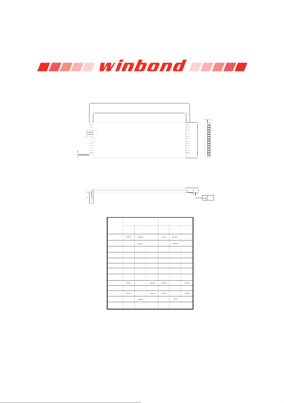
11 PACKAGING
11.1 28-LEAD 8X13.4MM PLASTIC THIN SMALL OUTLINE PACKAGE (TSOP) TYPE 1 - IQC
H
D
D
c
e
E
b
θ
L
1
L
Symbol
A
1
A
2
A
b
c
D
E
D
H
e
L
1
L
Y
θ
Dimension in Inches
Min.
Nom. Max. Min. Nom.
0.002
0.040
0.035
0.007 0.008 0.011
0.004
0.006
0.465 0.469
0.461
0.311 0.315 0.319
0.520 0.528 0.536
0.022
0.020
0.024
0.031
0.000
035
Dimension in mm
0.047
0.006
0.05
0.95
0.041
0.17
0.10
0.008
11.70
7.90
13.20
0.50
0.028
0.00
0.004
11.80
13.40
0
A
A
Max.
1.20
0.15
1.00
1.05
0.20 0.27
0.15 0.21
11.90
8.10
8.00
13.60
0.55
0.70
0.60
0.80
0.10
35
1
A
Y
2
Publication Release Date: January 23, 2007
- 19 - Revision 1.3-S2
Page 20

ISD1700 SERIES
11.2 28-L
EAD 300-MIL PLASTIC SMALL OUTLINE INTEGRATED CIRCUIT (SOIC)
27
26
2
25
24
4567
3
232221 20 19 18 171615
9101112 13
8
14
28
1
A
B
D
E
F
H
G
C
Plastic Small Outline Integrated Circuit (SOIC) Dimensions
INCHES MILLIMETERS
Min Nom Max Min Nom Max
A
B
C
D
E
F
G
H
Lead coplanarity to be within 0.004 inches.
Note:
0.701 0.706 0.711 17.81 17.93 18.06
0.097 0.101 0.104 2.46 2.56 2.64
0.292 0.296 0.299 7.42 7.52 7.59
0.005 0.009 0.0115 0.127 0.22 0.29
0.014 0.016 0.019 0.35 0.41 0.48
0.050 1.27
0.400 0.406 0.410 10.16 10.31 10.41
0.024 0.032 0.040 0.61 0.81 1.02
- 20 -
Page 21

ISD1700 SERIES
11.3 28-L
EAD 600-MIL PLASTIC DUAL INLINE PACKAGE (PDIP)
Plastic Dual Inline Package (PDIP) (P) Dimensions
Min Nom Max Min Nom Max
A 1.445 1.450 1.455 36.70 36.83 36.96
B1 0.150 3.81
B2 0.065 0.070 0.075 1.65 1.78 1.91
C1 0.600 0.625 15.24 15.88
C2 0.530 0.540 0.550 13.46 13.72 13.97
D 0.19 4.83
D1 0.015 0.38
E 0.125 0.135 3.18 3.43
F 0.015 0.018 0.022 0.38 0.46 0.56
G 0.055 0.060 0.065 1.40 1.52 1.65
H 0.100 2.54
J 0.008 0.010 0.012 0.20 0.25 0.30
S 0.070 0.075 0.080 1.78 1.91 2.03
0 0° 15° 0° 15°
INCHES
MILLIMETERS
11.4 D
For die info, please contact the local Winbond Sales Representatives.
Publication Release Date: January 23, 2007
- 21 - Revision 1.3-S2
IE INFORMATION
Page 22

12 ORDERING INFORMATION
Product Number Descriptor Key
ISD1700 SERIES
Product Name:
I = ISD
Product Series:
17 = 1700
Duration:
: 20 – 60 secs
30
: 26 – 80 secs
40
: 33 – 100 secs
50
: 40 – 120 secs
60
90
: 60 – 180 secs
120
: 80 – 240 secs
: 100 – 300 secs
150
180
: 120 – 360 secs
210
: 140 – 420 secs
: 160 – 480 secs
240
I17xxxxxxxxx
Package Type:
X = Die
E = Thin Small Outline Package (TSOP)
S = Small Outline Integrated Circuit
(SOIC) Package
P = Plastic Dual Inline Package (PDIP)
Special Features Field:
Blank = None
= vAlert
01
Tape & Reel:
Blank = None
R = Tape & Reel
Temperature:
I = Industrial (-40°C to +85°C)
Blank
= Commercial
• Die (0°C to +50°C)
• Package (0°C to +70°C)
Lead-Free:
Y = Lead-Free
When ordering ISD1700 devices, please refer to the above ordering scheme. Contact the local Winbond
Sales Representatives for any questions and the availability.
For the latest product information, please contact the Winbond Sales/Rep or
access Winbond’s worldwide web site at http://www.winbond-usa.com
- 22 -
Page 23

ISD1700 SERIES
13 VERSION HISTORY
VERSION DATE DESCRIPTION
1.3-S
1.3-S1
1.3-S2
Sep 2006
Nov 2006
Jan 2007
Initial version
Revise Pinout Configuration & Pin Description sections
Revise Rosc resistor value
Revise Selectable Message Duration section
Update standby current, sampling frequency & duration parameters
Publication Release Date: January 23, 2007
- 23 - Revision 1.3-S2
Page 24

ISD1700 SERIES
prop
Winbond products are not designed, intended, authorized or warranted for use as components in systems or equipment
intended for surgical implantation, atomic energy control instruments, airplane or spaceship instruments, transportation
instruments, traffic signal instruments, combustion control instruments, or for other applications intended to support or
sustain life. Furthermore, Winbond products are not intended for applications wherein failure of Winbond products could
result or lead to a situation wherein personal injury, death or severe property or environmental damage could occur.
Winbond customers using or selling these products for use in such applications do so at their own risk and agree to fully
indemnify Winbond for any damages resulting from such improper use or sales.
The contents of this document are provided only as a guide for the applications of Winbond products. Winbond makes no
representation or warranties with respect to the accuracy or completeness of the contents of this publication and
reserves the right to discontinue or make changes to specifications and product descriptions at any time without notice.
No license, whether express or implied, to any intellectual property or other right of Winbond or others is granted by this
publication. Except as set forth in Winbond's Standard Terms and Conditions of Sale, Winbond assumes no liability
whatsoever and disclaims any express or implied warranty of merchantability, fitness for a particular purpose or
infringement of any Intellectual property.
The contents of this document are provided “AS IS”, and Winbond assumes no liability whatsoever and disclaims any
express or implied warranty of merchantability, fitness for a particular purpose or infringement of any Intellectual
property. In no event, shall Winbond be liable for any damages whatsoever (including, without limitation, damages for
loss of profits, business interruption, loss of information) arising out of the use of or inability to use the contents of this
documents, even if Winbond has been advised of the possibility of such damages.
Application examples and alternative uses of any integrated circuit contained in this publication are for illustration only
and Winbond makes no representation or warranty that such applications shall be suitable for the use specified.
The 100-year retention and 100K record cycle projections are based upon accelerated reliability tests, as published in
the Winbond Reliability Report, and are neither warranted nor guaranteed by Winbond. This product incorporates
SuperFlash
This datasheet and any future addendum to this datasheet is(are) the complete and controlling ISD
product specifications. In the event any inconsistencies exist between the information in this and other product
documentation, or in the event that other product documentation contains information in addition to the information in
this, the information contained herein supersedes and governs such other information in its entirety. This datasheet is
subject to change without notice.
Copyright
Winbond Electronics Corporation. SuperFlash
are
®
.
®
ChipCorder®
©
2005, Winbond Electronics Corporation. All rights reserved. ChipCorder® and ISD® are trademarks of
erties of their respective owners.
®
is the trademark of Silicon Storage Technology, Inc. All other trademarks
- 24 -
 Loading...