

Page 1

ISD14B20
ISD14B20
SINGLE-CHIP, MULTIPLE-MESSAGE
VOICE RECORD/PLAYBACK DEVICE
10.6- TO 32-SECONDS DURATION
Publication Release Date: October 9, 2007
- 1 - Revision 0
Page 2

ISD14B20
TABLE OF CONTENTS
1. GENERAL DESCRIPTION ............................................................................................................... 3
2. FEATURES....................................................................................................................................... 3
3. BLOCK DIAGRAM ............................................................................................................................ 5
4. PAD DESCRIPTION ......................................................................................................................... 6
5. FUNCTIONAL DESCRIPTION ......................................................................................................... 8
5.1. Address Trigger (
NORM
) Operation ........................................................................................... 8
5.1.1. Record (
5.1.2. Edge-triggered Playback ( PlayE ) Operation ........................................................................ 10
5.1.3. Level- triggered Playback ( PlayL )Operation ........................................................................ 10
5.1.4. Playback (Supersedes Record) Operation .......................................................................... 11
5.1.5. XCLK Feature....................................................................................................................... 12
5.2. Direct Trigger (
5.3. Other Operations...................................................................................................................... 14
5.3.1. Rosc Operation .................................................................................................................... 14
LED
5.3.2.
5.3.3. Feed-Through mode Operation ........................................................................................... 15
5.3.4. Power-On Playback Operation ............................................................................................ 15
5.3.5. Automatic Single Message Playback................................................................................... 15
5.3.6. Power is interrupted Abruptly............................................................................................... 15
6. ABSOLUTE MAXIMUM RATINGS
6.1 Operating Conditions ................................................................................................................... 16
7. ELECTRICAL CHARACTERISTICS............................................................................................... 17
7.1. DC Parameters ........................................................................................................................... 17
7.2. AC Parameters ........................................................................................................................... 18
8. TYPICAL APPLICATION CIRCUIT ................................................................................................ 19
9. PACKAGING................................................................................................................................... 21
9.1 Die Information .......................................................................................................................... 21
10. ORDERING INFORMATION .......................................................................................................... 22
11. VERSION HISTORY....................................................................................................................... 23
REC
) Operation ........................................................................................................ 8
) Operation............................................................................................. 12
MODE
Operation...................................................................................................................... 15
[1]
.............................................................................................. 16
Publication Release Date: October 9, 2007
- 2 - Revision 0
Page 3

ISD14B20
1. GENERAL DESCRIPTION
Winbond’s ISD14B20 ChipCorder® is a new single-chip multiple-message record/playback series with dual
operating modes (address trigger and direct trigger) with wide operating voltage ranging from 2.4V to 5.5V. The
sampling frequency can be selected from 4 to 12 kHz via an external resistor, which also determines the duration
from 10.6 to 32 seconds. The device is designed for mostly standalone applications, and of course, it can be
manipulated by a microcontroller, if necessary.
The two operating modes are address trigger and direct trigger. While in address trigger mode, both record and
playback operations are manipulated according to the start address and end address specified through the start
address and end address pins. However, in direct trigger mode, the device can configure the memory up to as
many as eight equal messages, pending upon the fixed message configuration settings. With the record or
playback feature being pre-selected, each message can be randomly accessed via its message control pin.
The device has a selectable differential microphone input with AGC feature or single-ended analog
input, AnaIn, under feed-through mode. Its differential Class D PWM speaker driver can directly drive
a typical speaker or buzzer.
2. FEATURES
The ISD14B20 is a multiple messages record/playback device with two operational modes: address
trigger ( ) and direct trigger (
• Supply voltage: 2.4V to 5.5V.
• External resistor, Rosc, selects sampling frequency and duration.
• Mic+/Mic- : differential microphone inputs.
• AGC : automatic gain control for microphone preamp circuit.
•
• When both
• SP+/SP- : Class-D PWM differential speaker drivers.
•
• Automatically power down after each operation cycle.
• Playback takes precedence over the recording operation.
y Temperature option: 0°C to +50°C (die)
y Packaging: die only
NORM
Sampling Frequency 12 kHz 8 kHz 6.4 kHz 5.3 kHz 4 kHz
Rosc 53.3 KΩ 80 KΩ 100 KΩ 120 KΩ 160 KΩ
FT
: feed-through the AnaIn signal to the speaker outputs while AnaIn is converted from MIC+.
FT
and recording are active, device will record AnaIn signal into memory with AnaIn
signal output to speaker simultaneously.
LED
: during recording, LED is on.
). The analog inputs and the outputs are:
MODE
Publication Release Date: October 9, 2007
- 3 - Revision 0
Page 4

2.1. Address trigger operational mode
ISD14B20
• While in mode, flexible message duration is defined by start address and end
NORM
address.
Utilize four start addresses ( , , & ) and four end addresses ( , , & ) to
•
S0 S1 S2 S3 E0 E1 E2 E3
specific the message duration.
REC
•
•
: Level-hold or Edge-trigger (toggle on-off) recording from start to end addresses.
PLAYE
: Edge-trigger playback from start to end addresses and stops at EOM marker, if EOM
is prior to end address. Toggle on-off.
PLAYL
•
loop playback from start to end addresses.
: Level-hold playback from start to end addresses. Also, if constantly Low, device will
2.2. Direct trigger operational mode
• While
is active, utilizing, FMC1, &
MODE
FMC2
adapt various (1 to 8) fixed equal message configurations for random access and pre-defines
the fixed message duration accordingly.
• The control pins are:
M1
~M8 (message activation) and
• The record or playback operation is pre-defined by the
• Each message can be randomly accessed via its message control pin (
desired operation is facilitated accordingly.
FMC3
, the device reconfigures some pins to
/PR
(record or playback selection).
/PR
pin.
M1
~M8) and the
Publication Release Date: October 9, 2007
- 4 - Revision 0
Page 5
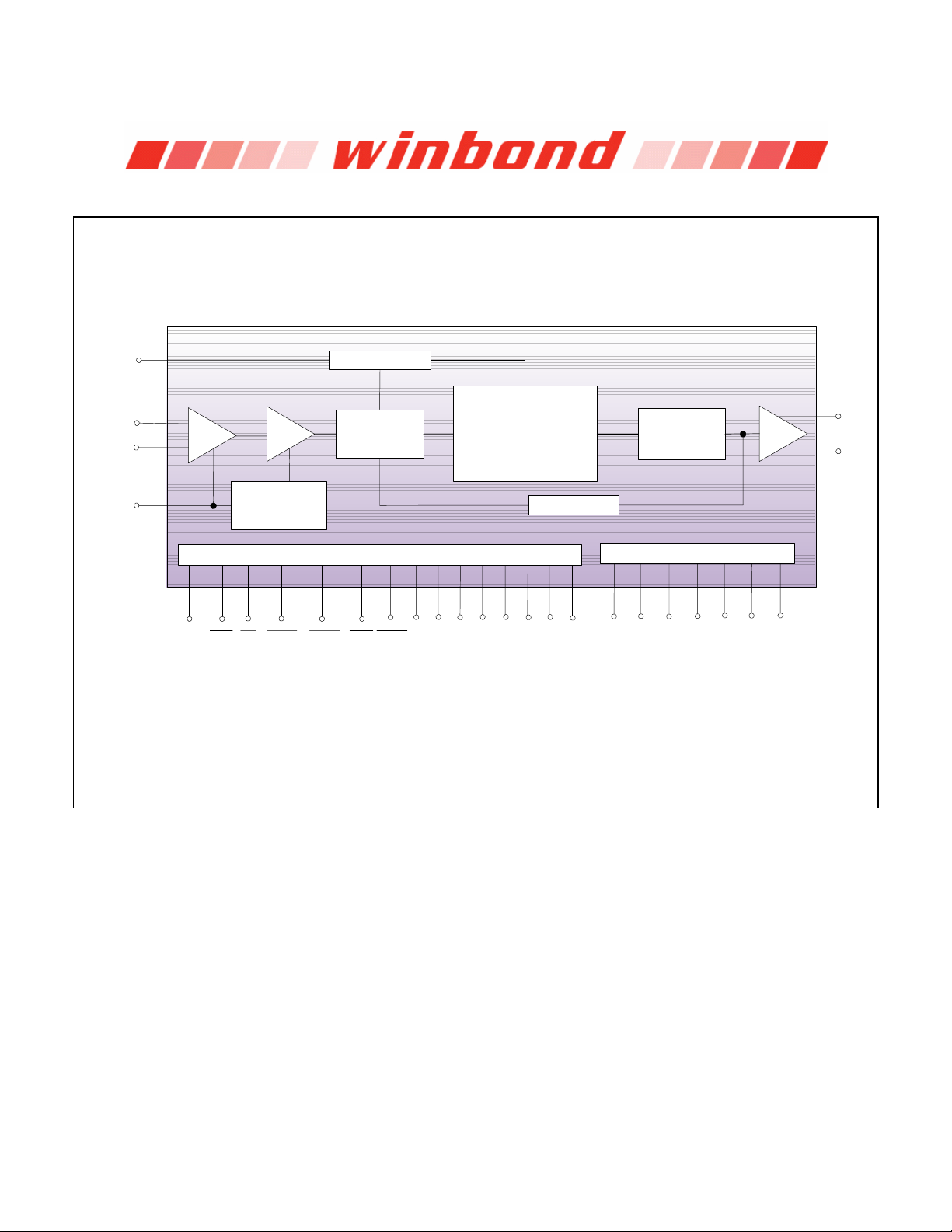
3. BLOCK DIAGRAM
ISD14B20
Rosc
MIC+_
AnaIn
AGC
Address Trigger:
Direct Trigger:
NORM
MODE
Pre-
Amp
LED
LED
Amp
Automatic
Gain Control
(AGC)
FT
FT
Clock Control
Antialiasing
Filter
Device & Address Control
PlayLPlayE
REC
FMC2FMC3
S0 S1 S2 S3 E0 E1 E2 E3
XCLK
M1 M2 M3R/P M8M6 M7FMC1
Non-Volatile
Multi Level Storage
Array
Switch
M4
M5
Smoothing
Filter
Power Conditioning
V
CCAVSSA
V
CCD
V
SSD
V
CCpVSSP1
Amp
V
SP +
SP -
SSP2
Publication Release Date: October 9, 2007
- 5 - Revision 0
Page 6
4. PAD DESCRIPTION
PAD NAME I / O FUNCTION
V
I
SSD
S0
/M1
S1
/M2
S2 /
M3
S3
M4
/
PLAYL
/ FMC1
E0
/M5
V
SSA
E1/
M6
E2
/M7
E3
/
M8
V
I
SSP2
SP- O
V
I
CCP
SP+ O
V
I
SSP1
AGC I
MIC+ / AnaIn I
Digital Ground: Ground path for digital circuits.
I
I
I
I
[1]
S0
: In Norm mode, Start Address Bit 0.
M1
: When
& debounce existed.
[1]
S1
: In Norm mode, Start Address Bit 1.
M2
: When
& debounce existed.
[1]
S2
: In Norm mode, Start Address Bit 2.
: When
M3
& debounce existed.
[1]
S3
: In Norm mode, Start Address Bit 3.
M4
: When
is active, low active operation on 1
MODE
is active, low active operation on 2
MODE
is active, low active operation on 3
MODE
is active, low active operation on 4
MODE
& debounce existed.
I
PLAYL
: In Norm mode, low active input, Level-hold playback start to end
addresses, debounce & internal pull-up existed. Holding
perform looping playback function from start to end addresses with insignificant
dead time between messages regardless of sampling frequencies.
FMC1 : When
various fixed-message configurations.
I
[1]
E0
: In Norm mode, End Address Bit 0.
: When
M5
MODE
is active, , together with FMC2 & , setup
MODE
FMC1
is active, low active operation on 5
& debounce existed.
I
Analog Ground: Ground path for analog circuits.
I
I
I
[1]
E1
: In Norm mode, End Address Bit 1.
: When
M6
& debounce existed.
[1]
E2
: In Norm mode, End Address Bit 2.
M7
: When
& debounce existed.
[1]
E3
: In Norm mode, End Address Bit 3.
: When
M8
is active, low active operation on 6
MODE
is active, low active operation on 7
MODE
is active, low active operation on 8
MODE
& debounce existed.
Ground: Ground for negative PWM speaker driver.
SP-: Negative signal of the differential Class-D PWM speaker outputs. This output,
together with the SP+, is used to drive an 8Ω speaker directly.
Speaker Power Supply: Power supply for PWM speaker drivers.
SP+: Positive signal of the differential Class-D PWM speaker outputs. This output,
together with the SP-, is used to drive an 8Ω speaker directly.
Ground: Ground for positive PWM speaker driver.
Automatic Gain Control (AGC): The AGC adjusts the gain of the microphone
preamplifier circuitry.
• MIC+ : Non-inverting input of the differential microphone signal.
• AnaIn : When
FT
is selected, the MIC+ input is configured to a single-ended
input with 1Vp-p maximum input amplitude and feed-through to the speaker
outputs.
ISD14B20
st
Message. Internal pull-up
nd
Message. Internal pull-up
rd
Message. Internal pull-up
th
Message. Internal pull-up
PLAYL
Low constantly will
FMC3
th
Message. Internal pull-up
th
Message. Internal pull-up
th
Message. Internal pull-up
th
Message. Internal pull-up
Publication Release Date: October 9, 2007
- 6 - Revision 0
Page 7
PAD NAME I / O FUNCTION
MIC- I
MIC- : Inverting input of the differential microphone signal. While
MIC- pin is disabled and must be floated.
Rosc I
Oscillator Resistor: Connect an external resistor from this pin to V
internal sampling frequency.
V
I
CCA
LED
Analog Power Supply: Power supply for analog circuits.
O
LED output: During recording, this output is Low. Also,
momentarily at the end of playback.
I
PLAYE
/ FMC2
PLAYE
: In Norm mode, low active input, edge-trigger playback from start to end
addresses & toggle on-off. Debounce & internal pull-up existed.
FMC2 : When
is active, , together with & , setup
MODE
FMC2 FMC1
various fixed-message configurations.
REC//PR
I
REC
: In Norm mode, level-hold (after 1 sec holding) or edge-trigger (toggle on-off),
low active, recording from start to end addresses. Debounce & internal pull-up
existed.
/PR
( When
• When
• When
/PR
/PR
is active):
MODE
is set to Low, level-hold record operation is selected.
is set to High, edge-trigger & toggle on-off playback operation is
selected.
XCLK
FMC3
/
I
External Clock: In Norm mode, low active and level-hold input. As
activated, Rosc pin accepts external clock input signal, provided resistor at Rosc
must be removed. Connecting this pin to High enables device running on internal
clock via Rosc resistor. If not used,
When
MODE
is active,
FMC3
XCLK
, together with & FMC2 , setup various fixed-
message configurations.
I
FT
Feed-Through : Low active input, Level-hold, debounce & Internal pull-up required.
FT
When
is selected, the MIC+ input is configured to a single-ended input with
1Vp-p maximum input amplitude and feed-through to the speaker outputs.
Norm /
MODE
I Level-hold input.
• Norm : When set to High, the device operates under Address trigger condition.
•
: When set to Low, the device operates under direct trigger condition. The
MODE
device reconfigures its pin definitions to fit various fixed-message configurations
utilizing ,FMC2 & pins as below table. FMC1
FMC3
FMC2 FMC1
FMC3
0 0 0 1
0 0 1 2
0 1 0 3
0 1 1 4
1 0 0 5
1 0 1 6
1 1 0 7
1 1 1 8
Digital Power Supply: Power supply for digital circuits.
Notes:
V
I
CCD
[1]
: Address bits , , , , , , & E3 are used to access the memory location.
S0 S1 S2 S3 E0 E1 E2
must be at high level.
FMC1
# of fixed messages
ISD14B20
FT
is enabled,
to select the
SSA
LED
pulses Low
FMC3
XCLK
Publication Release Date: October 9, 2007
- 7 - Revision 0
Page 8
5. FUNCTIONAL DESCRIPTION
ISD14B20
There are two operational modes: address trigger ( ) and direct trigger (
condition is selected on /
5.1. ADDRESS TRIGGER ( ) OPERATION
The start address bits ( , , & ) and end address bits ( , , & ) are used
NORM
NORM
S0 S1 S2 S3 E0 E1 E2 E3
, the power must be cycled to enable it.
MODE
NORM
). After a new
MODE
to access the memory location and they can divide the memory into a maximum of 16 slots. As
an example of I14B20, they are defined as follows:
S3
E3
( )
0 0 0 0 0 0
0 0 0 1 8 1.25
0 0 1 0 16 2.50
0 0 1 1 24 3.75
0 1 0 0 32 5.00
0 1 0 1 40 6.25
0 1 1 0 48 7.50
0 1 1 1 56 8.75
1 0 0 0 64 10.00
1 0 0 1 72 11.25
1 0 1 0 80 12.50
1 0 1 1 88 13.75
1 1 0 0 96 15.00
1 1 0 1 104 16.25
1 1 1 0 112 17.50
1 1 1 1 120 18.75
S2
E2
( )
S1
(E1)
S0
(E0)
Row # 14B20
Duration [s]
5.1.1. Record (
REC
) Operation
• Low active input, level-hold for level-trigger or falling edge for edge-trigger with debounce required.
• For 8kHz sampling frequency, if
recording is activated. However, if
REC
is held at Low for a period equal to 1 sec or more, then level
REC
is pulsed Low for less than 1 sec, then edge-trigger recording
is initiated.
• For 6.4kHz sampling frequency, if
level recording is activated. However, if
REC
is held at Low for a period equal to 1.25 sec or more, then
REC
is pulsed Low for less than 1.25 sec, then edge-trigger
recording is initiated.
• Recording begins from the start address to end address and
• Recording ceases whenever
REC
returns to High in level-hold mode or a subsequent lower going
LED
is on.
pulse appears while in edge-trigger mode or when end address is reached. Then an EOM marker is
written at the end of message. And
LED
is off.
• Then the device will automatically power down.
• This pin has an internal pull-up device.
• Once
REC
is active, input on FT, /
NORM
S0 S1 S2 S3 E0
, , , , , , , or is
MODE
E1 E2
E3
illegal.
Publication Release Date: October 9, 2007
- 8 - Revision 0
Page 9

ISD14B20
Fig. 1: Record–Level (
Norm/Mode
<S3:S0>
<E3:E0>
T
ASet
REC
T
Deb
LED
Mic+/-
or AnaIn
Fig. 2: Record–Level (
Norm/Mode
<S3:S0>
<E3:E0>
REC
LED
T
ASet
T
Deb
REC
) function till end address
T
AHold
REC
) function with start and stop actions
T
AHold
T
Deb
T
ASet
StopStart
T
Settle1
Start
T
T
Deb
AHold
T
Stop1
End Address
T
Mic+/-
Stop1
or AnaIn
Fig. 3: Record–Edge (
REC
) function with on-off
End Address
Norm/Mode
<S3:S0>
<E3:E0>
T
AHold
Start
T
Deb
REC
T
ASet
T
AHold
Start
T
Deb
T
Deb
Stop
T
ASet
T
Settle1
LED
T
Mic+/-
Stop1
or AnaIn
End Address
Publication Release Date: October 9, 2007
- 9 - Revision 0
Page 10

ISD14B20
5.1.2. Edge-triggered Playback (
PlayE ) Operation
• Low active input, edge-trigger, toggle on-off, debounce required.
• Playback begins from the start address to end address or EOM, whichever is occurred first.
• At the end of message,
LED
pulses Low momentarily.
• Then device will automatically power down.
• During playback, a subsequent trigger terminates the playback operation. If EOM marker is not encountered,
LED
then
will not pulses Low momentarily.
• This pin has an internal pull-up device.
T
Deb
REC, FT
T
ASet
Stop
T
Settle2
, /NORM
T
Start
T
AHold
Deb
, , , , , , ,
MODE
S0 S1 S2 S3 E0 E1 E2
T
EOM
End of
Message
• Once
PlayE is active, input on PlayL ,
E3
or is banned.
Fig. 4 : Playback–Edge (
Norm/Mode
<S3:S0>
<E3:E0>
PlayE
LED
Sp+
Sp-
PlayE ) function
T
ASet
T
Deb
T
Start
AHold
5.1.3. Level- triggered Playback (
)Operation
PlayL
• Low active input, Level-hold, debounce required.
• Once active, playback begins from the start address and stops whenever
an EOM is encountered,
LED
pulses Low momentarily.
returns to High. When
PlayL
• Then device will automatically power down.
• This pin has an internal pull-up device.
• Once
PlayL is active, input on PlayE ,
E3
or is prohibited.
Fig. 5: Playback–Level (
PlayL ) function
REC, FT
, /NORM
, , , , , , ,
MODE
S0 S1 S2 S3 E0 E1 E2
Publication Release Date: October 9, 2007
- 10 - Revision 0
Page 11
• However, holding
from start address to end address.
Norm/Mode
<S3:S0>
<E3:E0>
PlayL
LED
Sp+
Sp-
ISD14B20
T
ASet
T
AHold
T
ASet
StopStart
T
Deb
T
Deb
T
Settle2
Part of
Message
PlayL Low constantly will perform looping playback function, without power down,
T
AHold
Start
T
Deb
T
EOM
End of
Message
Fig. 6: Looping playback function via
PlayL
Norm/Mode
<S3:S0>
<E3:E0>
T
ASet
T
AHold
PlayL
T
Deb
T
EOM
T
EOM
LED
Sp+
Sp-
5.1.4. Playback (Supersedes Record) Operation
• Playback takes precedence over the Recording operation.
• If either
an EOM marker attached, and without power down, playback of the just-recorded message performs
accordingly. Then device powers down.
Fig. 7: An example of Playback supersedes Record
PlayE or PlayL is activated during a recording cycle, the recording immediately ceases with
Publication Release Date: October 9, 2007
- 11 - Revision 0
Page 12

Norm/Mode
<S3:S0>
<E3:E0>
Mic+/-
or AnaIn
REC
LED
PlayE
SP+
SP-
T
ASet
T
Deb
5.1.5. XCLK Feature
T
AHold
ISD14B20
T
EOM
T
T
Settle1
T
Deb
Settle3
• When precision sampling frequency is required, external clock mode can be activated by setting
XCLK
to Low. Under such condition, the resistor at Rosc pin must be removed and the external clock signal
must be applied to the Rosc pin. These conditions must be satisfied prior to any operations.
• However, when internal clock is used,
XCLK
must be linked to High.
• The external clock frequencies required for various sampling frequencies are listed in below table.
Sampling Freq [kHz] 12 8 6.4 5.3 4
XCLK
[MHz]
3.072 2.048 1.638 1.356 1.024
DIRECT TRIGGER (
5.2.
• The direct trigger is selected by the
allow the device to construct itself to the appropriate configuration by re-defining the function on the
related control pins. Also, the mode change is only allowed while the device is in power down state and
inhibited during an operation is in progress.
• Once direct trigger is activated, , & are utilized to select various (1 to 8) fixed
message configurations
message has approximate equal length of duration, which is related to the number of rows assigned as
in below table.
• The record or playback operation is pre-defined by the
operation while setting it to High enables playback operation.
• Each message can be randomly accessed via its message control pin (
operations are facilitated accordingly. Non-configured pins are automatically disabled and must be
floated.
[1]
Notes:
: Number of fixed message arrangement with respect to , &
FMC3
0 0 0 1
0 0 1 2
0 1 0 3
) OPERATION
MODE
pin. Once chosen, the supply voltage must be reset to
MODE
[1]
FMC1 FMC2
. Pending upon the arrangement on , &
FMC2 FMC1
FMC3
/PR
pin. Setting this pin to Low allows record
# of fixed messages
FMC1 FMC2
FMC3
, each divided
M1
~M8) and the desired
FMC3
. FMC1 FMC2
[1]
Publication Release Date: October 9, 2007
- 12 - Revision 0
Page 13

ISD14B20
0 1 1 4
1 0 0 5
1 0 1 6
1 1 0 7
[2]
: Number of memory row arrangement with respect to different number of fixed messages
[3]
: The durations for various fixed message configurations on I14B20 device at 8 kHz
1 1 1 8
for ISD14B20 (128 Rows). The non-configured Message control pins (Mx) will be disabled.
# of Msg M1 M2 M3 M4 M5 M6 M7 M8
1
2
3
4
5
6
7
8
sampling frequency are shown in below table.
# of Msg M1 M2 M3 M4 M5 M6 M7 M8
1
2
3
4
5
6
7
8
128
64 64
44 42 42
32 32 32 32
26 26 26 26 24
23 21 21 21 21 21
20 18 18 18 18 18 18
16 16 16 16 16 16 16 16
20
10 10
6.875 6.563 6.563
5.0 5.0 5.0 5.0
4.063 4.063 4.063 4.063 3.750
3.594 3.281 3.281 3.281 3.281 3.281
3.125 2.813 2.813 2.813 2.813 2.813 2.813
2.5 2.5 2.5 2.5 2.5 2.5 2.5 2.5
Publication Release Date: October 9, 2007
- 13 - Revision 0
Page 14

Example of four Fixed-Message Configuration:
Fig. 8: Record Operation under FMC mode
Norm/Mode
FM3
FM2
ISD14B20
FM1
R / P
M1 ~ M4
LED
Mic+/-
or AnaIn
Start
T
FSet
Stop
T
Settle1
T
Deb
T
Deb
T
Fig. 9: Playback Operation under FMC mode
Norm/Mode
FM3
FM2
FM1
T
R / P
M1 ~ M4
FSet
Start
Stop Start
Deb
Start
End of Duration
T
Stop1
T
EOM
LED
Sp+
Sp-
T
Deb
T
Settle2
T
Deb
T
Deb
End of Message
5.3. OTHER OPERATIONS
5.3.1. Rosc Operation
• When the R
accordingly.
Publication Release Date: October 9, 2007
- 14 - Revision 0
varies from 53.3 KΩ to 160 KΩ, the sampling frequency changes from 12 to 4 kHz
OSC
Page 15

ISD14B20
• When R
faster or slower.
• If the ground side of R
• The operation will resume when the resistor is connected back to ground.
5.3.2.
LED
•
be sufficiently greater than debounce time.
resistor value is changed during playback, the tone of a recorded message will alter either
OSC
resistor is floated or tied to VCC, then the current operation will be freezed.
OSC
LED
Operation
turns on during recording. Also,
LED
pulses Low at the end of message. The Low period must
5.3.3. Feed-Through mode Operation
• As FT is held Low, the Mic+ pin will be reconfigured as AnaIn input then the AnaIn signal will be
transmitted to the speaker outputs. Under this mode, Mic- pin is not used (must be floated).
• After
• If
• During an operation, activating the
FT
is enabled, If
Feed-Through path remains on.
FT
is already enabled, activating either PlayE or PlayL will first disable the FT path then play the
recorded message. Once playback completes, FT path will be resumed.
REC
is triggered, then AnaIn signal will be recorded into memory while the
FT
pin is not allowed.
5.3.4. Power-On Playback Operation
• If PlayE is kept at Low during power turns on, the device plays message once, then powers down.
• If PlayL is held at Low during power turns on and constantly maintained at Low, the device will play the
message repeatedly, with insignificant dead time between messages regardless of sampling
frequencies. This status will sustain unless power is turned off or
PlayL somehow returns to High.
5.3.5. Automatic Single Message Playback
LED
• If
is connected to PlayE , once PlayE is triggered, then the device plays message repeatedly
without power down between the looping playback. However, if
playback, then playback will stop.
PlayE is triggered again during
5.3.6. Power is interrupted Abruptly
• During the device is in operation, it is strongly recommended that the supply power cannot be
interrupted. Otherwise, it may cause the device to become malfunctioning.
Publication Release Date: October 9, 2007
- 15 - Revision 0
Page 16

ISD14B20
6. ABSOLUTE MAXIMUM RATINGS
ABSOLUTE MAXIMUM RATINGS
CONDITION VALUE
Junction temperature 150°C
Storage temperature range -65°C to +150°C
Voltage applied to any pins (VSS – 0.3V) to (VCC + 0.3V)
Voltage applied to Input pins (current limited to +/-20 mA) (VSS – 1.0V) to (VCC + 1.0V)
Voltage applied to output pins (current limited to +/-20 mA) (VSS – 1.0V) to (VCC + 1.0V)
[1]
VCC – V
SS
[1]
Stresses above those listed may cause permanent damage to the device. Exposure to the
absolute maximum ratings may affect device reliability and performance. Functional operation is
not implied at these conditions.
6.1 OPERATING CONDITIONS
Operating temperature range 0°C to +50°C
Operating voltage (VCC)
Ground voltage (VSS)
[1]
VCC = V
[2]
VSS = V
CCA
SSA
= V
= V
CCD
SSD
-0.3V to +7.0V
OPERATING CONDITIONS
CONDITION VALUE
[1]
[2]
+2.4V to +5.5V
0V
Publication Release Date: October 9, 2007
- 16 - Revision 0
Page 17
7. ELECTRICAL CHARACTERISTICS
7.1. DC PARAMETERS
PARAMETER SYMBOL MIN
Input Low Voltage V
Input High Voltage V
Output Low Voltage V
Output High Voltage V
Standby Current I
Record Current I
Playback Current I
Pull-up device for
PlayL ,
FT
REC
, PlayE ,
& M1~M8 pins
MIC+ Input Resistance R
MIC- Input Resistance R
AnaIn Input Resistance R
MIC Differential Input V
AnaIn Input V
Gain from MIC to SP+/- A
Output Load Impedance R
IL
IH
OL
OH
STBY
REC
PLAY
R
PU1
MICP
MICN
ANAIN
IN1
IN2
MSP
SPK
[2]
0.3xVcc V
0.7xVcc V
0.3xVcc V I
0.7xVcc V I
1 10 µA
20 30 mA V
20 30 mA V
18 KΩ
18 KΩ
42 KΩ
15 300 mV Peak-to-peak
1 V Peak-to-peak
6~40 dB
8 Ω Speaker load
Speaker Output Power Pout 313 mW
Speaker Output Voltage V
[1]
Notes:
Typical values @ VCC = 5.5V, TA = 25° and sampling frequency (Fs) at 8 kHz, unless stated.
[2]
Not all specifications are 100 percent tested. All Min/Max limits are guaranteed by Winbond via design,
electrical testing and/or characterization.
[3]
LED output during recording.
[4]
V
, V
CCD
and V
CCA
[5]
All required control pins must be at appropriate status. External components are biased under a separated
are connected together. Also, V
CCP
power supply.
OUT1
VDD V R
TYP
600
[1]
SSA
, V
MAX
SSD
, V
[2]
UNITS CONDITIONS
kΩ
and V
SSP1
SSP2
ISD14B20
= 4.0 mA
OL
= -1.6 mA
OH
[4] [5]
= 5.5V
CC
= 5.5V, no load
CC
VIN = 15~300 mVp-p,
AGC = 4.7 µF,
V
= 2.4V~5.5V
CC
V
= 4.4 V 1Vp-p,
DD
1 kHz sine wave at AnaIn.
R
= 8 Ω
SPK
= 8Ω Speaker,
SPK
Typical buzzer
are linked together.
[3]
[3]
[4] [5]
[4] [5]
Publication Release Date: October 9, 2007
- 17 - Revision 0
Page 18
ISD14B20
7.2. AC PARAMETERS
CHARACTERISTIC
[1]
SYMBOL MIN
Sampling Frequency Fs 4
Record Duration T
Playback Duration T
Debounce Time T
Address Setup Time T
Address Hold Time T
FMC Setup Time T
Record Settle Time T
Play Settle Time T
Delay from Record to Play T
Record Stop Time T
LED Pulse Low Time T
Notes:
[1]
Conditions are VCC = 5.5V, TA = 25°C and sampling frequency (FS) at 8kHz, unless specified.
[2]
Not all specifications are 100 percent tested. All Min/Max limits are guaranteed by Winbond via design,
electrical testing and/or characterization.
[3]
When different FS is applied, the value will change accordingly. Also, stability of internal oscillator may
vary as much as
[4]
k = 1000.
+10% over the operating temperature and voltage ranges.
REC
PLAY
Deb
ASet
AHold
FSet
Settle1
Settle2
Settle3
Stop1
EOM
[2]
TYP MAX
10.6 32 sec
10.6 32 sec
225k/F
msec
[2]
UNIT
S
12 kHz
[3]
[3]
[3]
[3] [4]
s
30 nsec
225k/F
msec
[3] [4]
s
30 nsec
32k/Fs msec
256k/F
msec
s
128k/F
msec
[3] [4]
[3] [4]
[3] [4]
s
30 nsec
256k/F
msec
[3] [4]
s
CONDITIONS
8.
Publication Release Date: October 9, 2007
- 18 - Revision 0
Page 19

ISD14B20
8. TYPICAL APPLICATION CIRCUIT
The following typical application examples on ISD14B20 series are for references only. They make
no representation or warranty that such applications shall be suitable for the use specified. It’s
customer’s obligation to verify the design in its own system for the functionalities, voice quality,
current consumption, and etc.
In addition, the below notes apply to the following application examples:
* The suggested values are for references only. Depending on system requirements, they can
be adjusted for functionalities, voice quality and degree of performance.
It is important to have a separate path for each ground and power back to the related terminals to
minimize the noise. Besides, the power supplies should be decoupled as close to the device as
possible.
Also, it is crucial to follow good audio design practices in layout and power supply decoupling. See
recommendations in Application Notes from our websites.
Example #1: Operations via start and end addresses under address trigger mode ( )
NORM
NORM
LED
XCLK
V
CCD
V
SSD
V
CCA
V
SSA
V
CCP
V
SSP1
V
SSP2
SP+
SP-
μ
0.1 F
1 KΩ
0.1 F
V
CCA
0.1 F
10 F*
D1
μ
μ
μ
Speaker
Vcc Gnd
V
CCA
V
10 F*
10 F*
V
CCP
μ
10 F*
CCD
V
CCP
μ
μ
V
CCD
μ
0.1 F
To switches or
address I/Os
V
CC
4.7 kΩ∗
Ω∗4.7 k
4.7 k
Ω∗
μ
4.7 F*
μ
0.1 F*
μ
0.1 F*
4.7 F*
μ
Rosc*
REC
PLAYE
PLAYL
S3
S2
S1
S0
E3
E2
ISD1916
E1
E0
FT
Mic+_AnaIn
Mic-
AGC
Rosc
Publication Release Date: October 9, 2007
- 19 - Revision 0
Page 20

ISD14B20
Example #2: Fixed Message Configuration Operations under direct trigger mode (
V
4.7 kΩ∗
CC
R/P
M1
M2
M3
M4
M5
M6
V
CC
μ
4.7 F*
Ω∗4.7 k
μ
0.1 F*
μ
0.1 F*
μ
4.7 k
Ω∗
4.7 F*
Rosc*
M7
M8
ISD14B20
FT
Mic+_AnaIn
Mic-
AGC
Rosc
LED
MODE
FMC3
FMC2
FMC1
V
CCD
V
SSD
V
CCA
V
SSA
V
CCP
V
SSP1
V
SSP2
SP+
SP-
0.1 F
1 k Ω
μ
μ
0.1 F
V
CCA
μ
0.1 F
10 F*
D1
V
μ
Speaker
CCD
0.1 F
μ
10 F*
μ
10 F
V
CCP
μ
10 F*
μ
MODE
Vcc Gnd
V
CCA
V
CCD
V
CCP
)
Good Audio Design Practices
Winbond’s ChipCorder are very high-quality single-chip voice recording and playback devices. To
ensure the highest quality voice reproduction, it is important that good audio design practices on
layout and power supply decoupling are followed. See Application Information links below for details.
Good Audio Design Practices
http://www.winbond-usa.com/products/isd_products/chipcorder/applicationinfo/apin11.pdf
Single-Chip Board Layout Diagrams
http://www.winbond-usa.com/products/isd_products/chipcorder/applicationinfo/apin12.pdf
It is strongly recommended that before any design or layout project starts, the designer should contact
Winbond Sales Rep for the most update technical information and layout advice.
Publication Release Date: October 9, 2007
- 20 - Revision 0
Page 21

9. PACKAGING
9.1 DIE INFORMATION
S2 / M3
S1 / M2
S0 / M1
ISD14B20
Norm / MODE
SSD
V
CCD
FT XCLK / FMC3
REC / R/P
V
S3 / M4
PLAYL / FMC1
E0 / M5
V
SSA
E1 / M6
E2 / M7
E3 / M8
ISD14B20
PLAYE / FMC2
LED
V
CCA
Rosc
V
CCA
Mic-
V
SSP2
V
CCP
SP+SP-
V
SSP1
AGC
Mic+_AnaIn
Contact Winbond Sales Representatives for other information.
Publication Release Date: October 9, 2007
- 21 - Revision 0
Page 22

10. ORDERING INFORMATION
Product Number Descriptor Key
ISD14B20
I14Bxxxx
Product Name:
I = ISD
Product Series:
14B = 14B00
Duration:
20
: 10.6 – 32 secs
When ordering ISD14B20 devices, please refer to the above ordering scheme. Contact the local Winbond
Sales Representatives for any questions and the availability.
For the latest product information, please contact the Winbond Sales/Rep or
access Winbond’s worldwide web site at
Package Type:
X = Die
http://www.winbond-usa.com
Temperature:
Blank
= Commercial
• Die (0°C to +50°C)
Publication Release Date: October 9, 2007
- 22 - Revision 0
Page 23

11. VERSION HISTORY
VERSION DATE DESCRIPTION
0 Oct 9, 2007 Initial revision
ISD14B20
Publication Release Date: October 9, 2007
- 23 - Revision 0
Page 24

ISD14B20
prop
Winbond products are not designed, intended, authorized or warranted for use as components in systems or equipment
intended for surgical implantation, atomic energy control instruments, airplane or spaceship instruments, transportation
instruments, traffic signal instruments, combustion control instruments, or for other applications intended to support or
sustain life. Furthermore, Winbond products are not intended for applications wherein failure of Winbond products could
result or lead to a situation wherein personal injury, death or severe property or environmental damage could occur.
Winbond customers using or selling these products for use in such applications do so at their own risk and agree to fully
indemnify Winbond for any damages resulting from such improper use or sales.
The contents of this document are provided only as a guide for the applications of Winbond products. Winbond makes no
representation or warranties with respect to the accuracy or completeness of the contents of this publication and
reserves the right to discontinue or make changes to specifications and product descriptions at any time without notice.
No license, whether express or implied, to any intellectual property or other right of Winbond or others is granted by this
publication. Except as set forth in Winbond's Standard Terms and Conditions of Sale, Winbond assumes no liability
whatsoever and disclaims any express or implied warranty of merchantability, fitness for a particular purpose or
infringement of any Intellectual property.
The contents of this document are provided “AS IS”, and Winbond assumes no liability whatsoever and disclaims any
express or implied warranty of merchantability, fitness for a particular purpose or infringement of any Intellectual
property. In no event, shall Winbond be liable for any damages whatsoever (including, without limitation, damages for
loss of profits, business interruption, loss of information) arising out of the use of or inability to use the contents of this
documents, even if Winbond has been advised of the possibility of such damages.
Application examples and alternative uses of any integrated circuit contained in this publication are for illustration only
and Winbond makes no representation or warranty that such applications shall be suitable for the use specified.
The 100-year retention and 100K record cycle projections are based upon accelerated reliability tests, as published in
the Winbond Reliability Report, and are neither warranted nor guaranteed by Winbond. This product incorporates
SuperFlash
Information contained in this ISD
published by ISD
This datasheet and any future addendum to this datasheet is(are) the complete and controlling ISD
product specifications. In the event any inconsistencies exist between the information in this and other product
documentation, or in the event that other product documentation contains information in addition to the information in
this, the information contained herein supersedes and governs such other information in its entirety. This datasheet is
subject to change without notice.
Copyright
Winbond Electronics Corporation. SuperFlash
are
®
.
®
®
prior to August, 1998.
©
2005, Winbond Electronics Corporation. All rights reserved. ChipCorder® and ISD® are trademarks of
erties of their respective owners.
ChipCorder® datasheet supersedes all data for the ISD ChipCorder products
®
ChipCorder®
®
is the trademark of Silicon Storage Technology, Inc. All other trademarks
Please note that all data and specifications are subject to change without notice.
All the trademarks of products and companies mentioned in this datasheet belong to their respective owners.
Publication Release Date: October 9, 2007
- 24 - Revision 0
 Loading...