

Page 1
Q
Absolute Maximum Ratings
V
ID @ TA = 25°C
Continuous Drain Current, V
@ 4.5V
Continuous Drain Current, V
@ 4.5V
Pulsed Drain Current
c
PD @TA = 25°C
T
Note
Form
Quantity
IRFTS9342TRPbF
TSOP-6
Tape and Reel
3000
Features
Benefits
Industry-Standard TSOP-6 Package
Multi-Vendor Compatibility
⇒
MSL1, Consumer Qualification
Increased Reliability
PD - 96411A
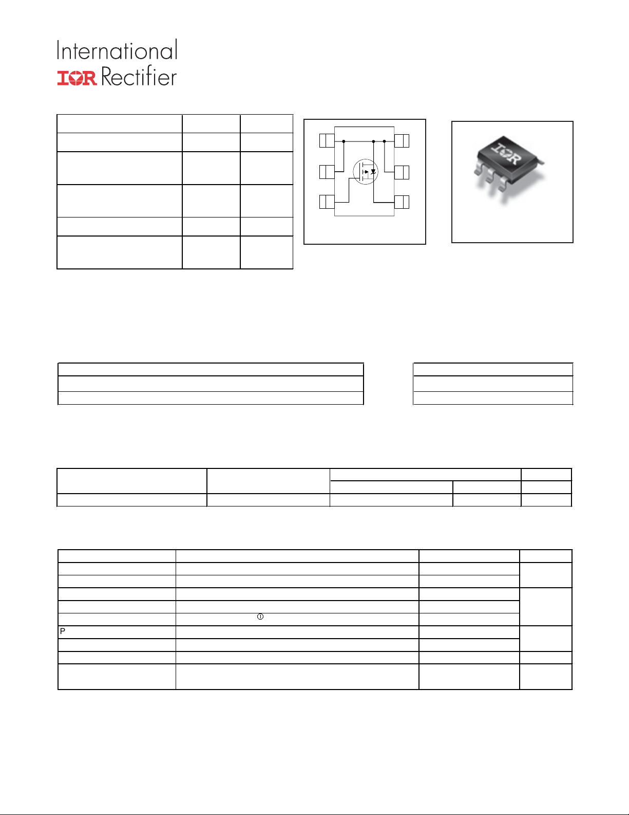
IRFTS9342PbF
HEXFET® Power MOSFET
V
DS
V
GS max
R
DS(on) max
(@VGS = -10V)
R
DS(on) max
(@VGS = -4.5V)
g typ
I
D
(@TA= 25°C)
-30 V
20 V
±
40
66
12
m
m
nC
-5.8 A
Ω
Ω
D
D
G
1
2
3
Top View
Applications
l Battery operated DC motor inverter MOSFET
l System/Load Switch
Features and Benefits
RoHS Compliant Containing no Lead, no Bromide and no Halogen
6
5
4
results in
A
D
D
S
TSOP-6
Environmentally Friendlier
Orderable part number Package Type Standard Pack
Parameter Units
DS
V
GS
ID @ TA = 70°C
I
DM
@TA = 70°C
P
D
T
J
STG
Drain-to-Source Voltage
Gate-to-Source Voltage
GS
GS
Power Dissipation
Power Dissipation
Linear Derating Factor W/°C
Operating Junction and
Storage Temperature Range
Notes through are on page 2
Max.
-30
±20
-5.8
-4.6
-46
2.0
1.3
0.02
-55 to + 150
V
A
W
°C
www.irf.com 1
02/29/12
Page 2
IRFTS9342PbF
Thermal Resistance
θ
JA
Parameter
Min.
Typ.
Max.
Units
BV
ΔΒ
V
/ΔT
R
V
Δ
V
I
I
Q
Q
Q
–––
t
t
t
t
C
C
C
Diode Characteristics
Parameter
Min.
Typ.
Max.
Units
I
I
(Body Diode)
V
t
Q
t
Ω
di/dt = 100A/μs
e
Static @ TJ = 25°C (unless otherwise specified)
DSS
DSS
J
DS(on)
GS(th)
GS(th)
DSS
GSS
gfs Forward Transconductance 6.8 ––– ––– S
g
gs
gd
R
G
d(on)
r
d(off)
f
iss
oss
rss
Drain-to-Source Breakdown Voltage -30 ––– ––– V
Breakdown Voltage Temp. Coefficient ––– 19 ––– mV/°C
Static Drain-to-Source On-Resistance ––– 32 40
––– 53 66
Gate Threshold Voltage -1.3 ––– -2.4 V
Gate Threshold Voltage Coefficient ––– -5.5 ––– mV/°C
Drain-to-Source Leakage Current ––– ––– -1.0
––– ––– -150
Gate-to-Source Forward Leakage ––– ––– -100
Gate-to-Source Reverse Leakage ––– ––– 100
Total Gate Charge
Gate-to-Source Charge
Gate-to-Drain Charge
––– 12 –––
––– 1.8 –––
––– 3.1 –––
Gate Resistance ––– 17
Turn-On Delay Time ––– 4.6 –––
Rise Time ––– 13 –––
Turn-Off Delay Time ––– 45 –––
Fall Time ––– 28 –––
Input Capacitance ––– 595 –––
Output Capacitance ––– 133 –––
Reverse Transfer Capacitance ––– 85 –––
VGS = 0V, ID = -250μA
Reference to 25°C, I
= -10V, ID = -5.8A
V
GS
mΩ
V
= -4.5V, ID = -4.6A
GS
= VGS, ID = -25μA
V
DS
= -24V, VGS = 0V
V
DS
μA
nA
= -24V, VGS = 0V, TJ = 125°C
V
DS
= -20V
V
GS
= 20V
V
GS
VDS = -10V, ID = -4.6A
= -15V
V
DS
= -10V
V
nC
GS
I
= -4.6A
D
Ω
V
= -15V, VGS = -10V
DD
I
= -4.6A
D
ns
R
= 6.8
G
V
= 0V
GS
= -25V
V
pF
DS
ƒ = 1.0KHz
Conditions
= -1mA
D
e
e
S
Continuous Source Current
(Body Diode)
SM
Pulsed Source Current
c
SD
rr
rr
on
Diode Forward Voltage ––– ––– -1.2 V
Reverse Recovery Time ––– 20 30 ns
Reverse Recovery Charge ––– 11 17 nC
Forward Turn-On Time Time is dominated by parasitic Inductance
Parameter Typ. Max. Units
R
Notes:
Junction-to-Ambient
e
Repetitive rating; pulse width limited by max. junction temperature.
Pulse width ≤ 400μs; duty cycle ≤ 2%.
When mounted on 1 inch square copper board.
––– ––– -2.0
––– ––– -46
Conditions
MOSFET symbol
showing the
A
integral reverse
p-n junction diode.
TJ = 25°C, IS = -4.6A, VGS = 0V
T
= 25°C, IF = -4.6A, VDD = -24V
J
––– 62.5 °C/W
D
G
S
e
2 www.irf.com
Page 3
IRFTS9342PbF
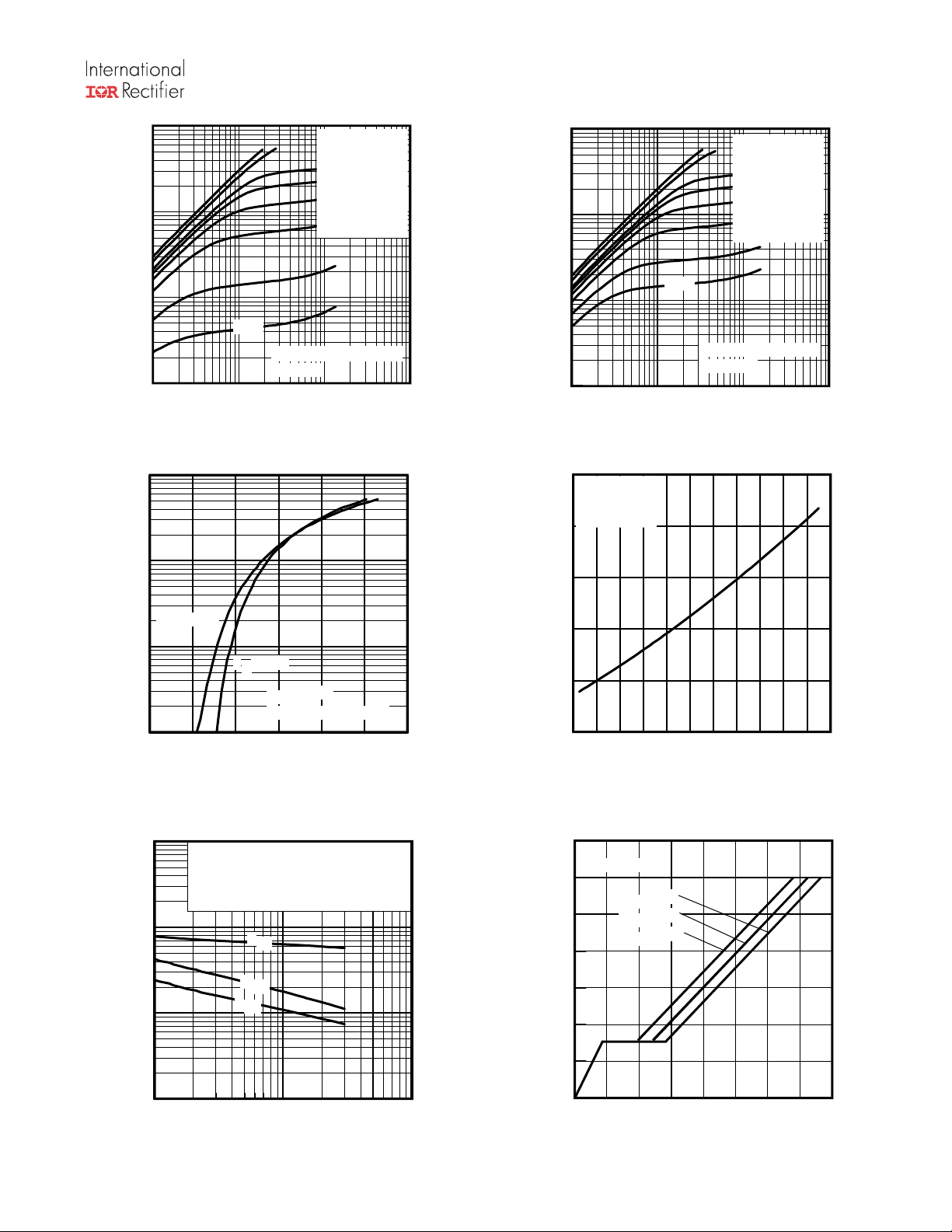
100
TOP -10V
)
A
(
t
n
e
r
r
10
u
C
e
c
r
u
o
S
o
t
n
1
i
a
r
D
,
D
I
-
-2.8V
≤
0.1
Tj = 25°C
BOTTOM -2.8V
60μs PULSE WIDTH
0.1 1 10 100
-VDS, Drain-to-Source Voltage (V)
Fig 1. Typical Output Characteristics
100
)
A
(
t
n
e
r
r
10
u
C
e
c
r
u
o
S
o
t
n
i
a
r
D
,
I
-
D
TJ = 150°C
1
TJ = 25°C
V
DS
= -15V
≤60μs PULSE WIDTH
0.1
1 2 3 4 5 6 7
-VGS, Gate-to-Source Voltage (V)
Fig 3. Typical Transfer Characteristics
VGS
-7.0V
-5.0V
-4.5V
-4.0V
-3.5V
-3.0V
100
TOP -10V
)
A
(
t
n
e
r
r
10
u
C
e
c
r
u
o
S
o
t
n
1
i
a
r
D
,
D
I
-
-2.8V
BOTTOM -2.8V
60μs PULSE WIDTH
≤
VGS
-7.0V
-5.0V
-4.5V
-4.0V
-3.5V
-3.0V
Tj = 150°C
0.1
0.1 1 10 100
-VDS, Drain-to-Source Voltage (V)
Fig 2. Typical Output Characteristics
1.6
e
c
n
a
t
s
i
s
e
R
n
O
e
c
r
u
o
S
o
t
n
i
a
r
D
,
)
n
o
(
S
D
R
)
d
e
z
i
l
a
m
r
o
N
(
1.4
1.2
1.0
0.8
ID = -5.8A
V
= -10V
GS
0.6
-60 -40 -20 0 20 40 60 80 100 120 140160
TJ , Junction Temperature (°C)
Fig 4. Normalized On-Resistance vs. Temperature
10000
)
F
1000
p
(
e
c
n
a
t
i
c
a
p
a
C
,
C
100
V
= 0V, f = 1 MHZ
GS
C
= C
iss
rss
oss
= C
= C
gs
gd
ds
C
C
C
C
oss
C
rss
+ Cgd, C
+ C
gd
iss
SHORTED
ds
10
1 10 100
-VDS, Drain-to-Source Voltage (V)
Fig 5. Typical Capacitance vs.Drain-to-Source Voltage
Fig 6. Typical Gate Charge vs.Gate-to-Source Voltage
14.0
)
12.0
V
(
e
g
a
10.0
t
l
o
V
e
c
r
u
o
S
o
t
e
t
a
G
,
S
G
V
-
ID= -4.6A
VDS= -24V
VDS= -15V
VDS= -6.0V
8.0
6.0
4.0
2.0
0.0
0246810121416
Q
Total Gate Charge (nC)
G
www.irf.com 3
Page 4

IRFTS9342PbF
100
)
A
(
t
n
e
r
r
10
u
C
n
i
a
r
D
e
s
r
e
v
e
R
,
D
S
I
-
0.1
TJ = 150°C
TJ = 25°C
1
V
= 0V
GS
0.4 0.6 0.8 1.0 1.2 1.4
-VSD, Source-to-Drain Voltage (V)
Fig 7. Typical Source-Drain Diode Forward Voltage
6
5
)
A
(
4
t
n
e
r
r
u
C
3
n
i
a
r
D
,
2
D
I
-
1
0
25 50 75 100 125 150
TA , Ambient Temperature (°C)
Fig 9. Maximum Drain Current vs.
Case Temperature
100
D = 0.50
W
/
10
C
°
)
A
J
h
t
1
Z
(
e
s
n
o
p
0.1
s
e
R
l
a
m
r
e
0.01
h
T
0.001
1E-006 1E-005 0.0001 0.001 0.01 0.1 1 10 100
0.20
0.10
0.05
0.02
0.01
SINGLE PULSE
( THERMAL RESPONSE )
t1 , Rectangular Pulse Duration (sec)
1000
OPERATION IN THIS AREA
)
A
100
(
t
n
e
r
r
u
C
10
e
c
r
u
o
S
-
1
o
t
n
i
a
r
D
,
0.1
D
I
Tc = 25°C
Tj = 150°C
Single Pulse
0.01
0.01 0.1 1 10 100
VDS, Drain-to-Source Voltage (V)
LIMITED BY RDS(on)
100μsec
1msec
10msec
DC
Fig 8. Maximum Safe Operating Area
3.0
2.8
)
V
(
e
2.6
g
a
t
l
o
2.4
V
d
l
2.2
o
h
s
e
2.0
r
h
t
e
t
1.8
a
G
,
)
h
t
(
S
G
V
-
ID = -25μA
ID = -250μA
1.6
ID = -1.0mA
ID = -10mA
1.4
ID = -1.0A
1.2
1.0
-75 -50 -25 0 25 50 75 100 125 150
TJ , Temperature ( °C )
Fig 10. Threshold Voltage vs. Temperature
Notes:
1. Duty Factor D = t1/t2
2. Peak Tj = P dm x Zthja + T
A
Fig 11. Maximum Effective Transient Thermal Impedance, Junction-to-Case
4 www.irf.com
Page 5

IRFTS9342PbF
)
100
Ω
m
(
e
c
n
80
a
t
s
i
s
e
R
n
60
O
e
c
r
u
o
S
-
40
o
t
n
i
a
r
D
20
,
)
n
o
(
S
D
0
R
TJ = 125°C
ID = -5.8A
TJ = 25°C
2 4 6 8 10 12 14 16 18 20
-V
Gate -to -Source Voltage (V)
GS,
Fig 12. On-Resistance vs. Gate Voltage
120
)
J
m
(
y
100
g
r
e
n
E
e
80
h
c
n
a
l
a
v
60
A
e
s
l
u
P
40
e
l
g
n
i
S
,
20
S
A
E
0
25 50 75 100 125 150
Starting TJ , Junction Temperature (°C)
TOP -0.91A
BOTTOM -4.6A
I
D
-1.4A
)
220
Ω
m
(
200
e
c
n
a
180
t
s
i
s
e
160
R
n
O
e
c
r
u
o
S
o
t
n
i
a
r
D
,
)
n
o
(
S
D
R
140
120
100
80
60
40
20
Vgs = -4.5V
Vgs = -10V
0 10 20 30 40 50
-ID, Drain Current (A)
Fig 13. Typical On-Resistance vs. Drain Current
100
90
80
70
)
60
W
(
r
50
e
w
o
40
P
30
20
10
0
0.0001 0.001 0.01 0.10 1 10
Time (sec)
Fig 14. Maximum Avalanche Energy vs. Drain Current Fig 15. Typical Power vs. Time
D.U.T *
+
+
Circuit Layout Considerations
• Low Stray Inductance
• Ground Plane
-
• Low Leakage Inductance
Current Transformer
-
-
R
G
• di/dt controlled by R
• Driver same type as D.U.T.
• ISD controlled by Duty Factor "D"
• D.U.T. - Device Under Test
G
* Reverse Polarity of D.U.T for P-Channel
Driver Gate Drive
P.W.
D.U.T. ISDWaveform
Reverse
Recovery
+
V
DD
+
-
Current
Re-Applied
Voltage
D.U.T. VDSWaveform
Inductor Current
Inductor Curent
* V
GS
Period
Body Diode Forward
Current
di/dt
Diode Recovery
dv/dt
Body Diode Forward Drop
Ripple ≤ 5%
= 5V for Logic Level Devices
D =
P. W .
Period
VGS=10V
V
DD
I
SD
*
Fig 16. Diode Reverse Recovery Test Circuit for P-Channel HEXFET® Power MOSFETs
www.irf.com 5
Page 6

IRFTS9342PbF
A
(BR)
0
20K
1K
DUT
Fig 17a. Gate Charge Test Circuit
R
-V
-20V
V
DS
G
GS
t
p
D.U.T
I
AS
L
0.01
DRIVER
Ω
Id
Vgs
Vds
L
VCC
Vgs(th)
Qgs1
Qgs2QgdQgodr
Fig 17b. Gate Charge Waveform
I
AS
V
DD
15V
Fig 18a. Unclamped Inductive Test Circuit
R
V
V
GS
R
G
-V
GS
Pulse Width ≤ 1 µs
Duty Factor ≤ 0.1 %
DS
D
D.U.T.
t
p
V
DSS
Fig 18b. Unclamped Inductive Waveforms
t
d(on)tr
V
GS
10%
-
V
+
DD
90%
V
DS
t
d(off)tf
Fig 19a. Switching Time Test Circuit
Fig 19b. Switching Time Waveforms
6 www.irf.com
Page 7

TSOP-6 Package Outline
IRFTS9342PbF
TSOP-6 Part Marking Information
Y = YEAR
W = WE E K
PAR T NUMBER
LOT
TOP
PART NUMBER CODE RE FE RE NCE:
A = S I3443DV
B = IRF5800
C = IR F58 5 0
D = IR F5851
E = IRF5852
O = I RL TS 6342TR PBF
P = IR F T S8342T RPB F
R = IR F T S9342 T RPB F
S = Not applicable
T = IRL T S2242T RPB F
F = IRF5801
G = I RF5803
H = IRF 5804
I = IRF 5805
J = IR F 5806
K = IRF 5 810
N = IRF 5802
Note: A li ne above the work week
(as shown here) indicates Lead-Free.
CODE
DATE CODE MARKING INSTRUCTIONS
WW = (1-26) IF PRECEDED BY LAST DIGIT OF CALENDAR YEAR
1
2
3
4
5
6
7
8
9
02010
Y
A
B
C
D
E
F
G
H
J
K
WOR K
01
02
03
04
25
26
WOR K
WEEK
27
28 B
30 D
50
51
A
B
C
D
X24
Y
Z
W
A
C29
X
Y
Z52
YEAR Y WWEEK
2011
2001
2012
2002
2013
2003
2014
2004
2015
2005
2016
2006
2017
2007
2018
2008
2019
2009
2020
WW = (27-52) IF P RE CEDED B Y A LE T T E R
YEAR
2001
2011
2002
2012
2003
2013
2004
2014
2005
2015
2006
2016
2007
2017
2008
2018
2009
2019
2010
2020
Note: For the most current drawing please refer to IR website at: http://www.irf.com/package/
www.irf.com 7
Page 8

IRFTS9342PbF
TSOP-6 Tape and Reel Information
8mm
FEED DIRECTION
9.90 ( .390 )
8.40 ( .331 )
Cons umer
NOTES :
1. OUTLINE CONFORMS TO EIA-481 & EIA-541.
178.00
( 7.008 )
MAX.
NOTES:
1. CONTROLLING DIMENSION : MILLIMETER.
2. OUTLINE CONFORMS TO EIA-481 & EIA-541.
Qualification information
Qualification level
4mm
†
(per JE DEC JES D47F
Moisture Sensitivity Level
TSOP-6
(per I P C/JE DE C J-S T D- 02 0 D
RoHS compliant Yes
††
†††
guidelines )
MS L 1
†††
)
† Qualification standards can be found at International Rectifier’s web site
http://www.irf.com/product-info/reliability
†† Higher qualification ratings may be available should the user have such requirements.
Please contact your International Rectifier sales representative for further information:
http://www.irf.com/whoto-call/salesrep/
††† Applicable version of JEDEC standard at the time of product release.
Data and specifications subject to change without notice.
IR WORLD HEADQUARTERS: 101 N. Sepulveda Blvd., El Segundo, California 90245, USA Tel: (310) 252-7105
TAC Fax: (310) 252-7903
Visit us at www.irf.com for sales contact information. 02/2012
8 www.irf.com
 Loading...