

Page 1
1K 3-Wire CMOS Serial EEPROM
Features
•
Operating voltage V
–
Read: 2.0V~5.5V
–
Write: 2.4V~5.5V
•
Low power consumption
–
Operating: 5mA max.
–
Standby: 10µA max.
•
User selectable internal organization
–
1K(HT93LC46): 128×8 or 64×16
•
3-wire Serial Interface
•
Write cycle time: 2ms max.
General Description
The HT93LC46 is a 1K-bit low voltage nonvolatile, serial electrically erasable programmable
read only memory device using the CMOS floating gate process. Its 1024 bits of memory are
organized into 64 words of 16 bits each when the
ORG pin is connected to VCC or organized into
128 words of 8 bits each when it is tied to VSS. The
CC
HT93LC46
•
Automatic erase-before-write operation
•
Word/chip erase and write operation
•
Write operation with built-in timer
•
Software controlled write protection
•
10-year data retention after 100K rewrite
cycles
•
106 rewrite cycles per word
•
8-pin DIP/SOP package
•
Commercial temp erature range
(0
°C to +70°C)
device is optimized for use in many industrial
and commercial applications where low power
and low voltage operation are essential. By
popular microcontroller, the versatile serial interface including chip select (CS), serial clock
(SK), data inpu t (DI) and data out put (DO) can
be easily controlled.
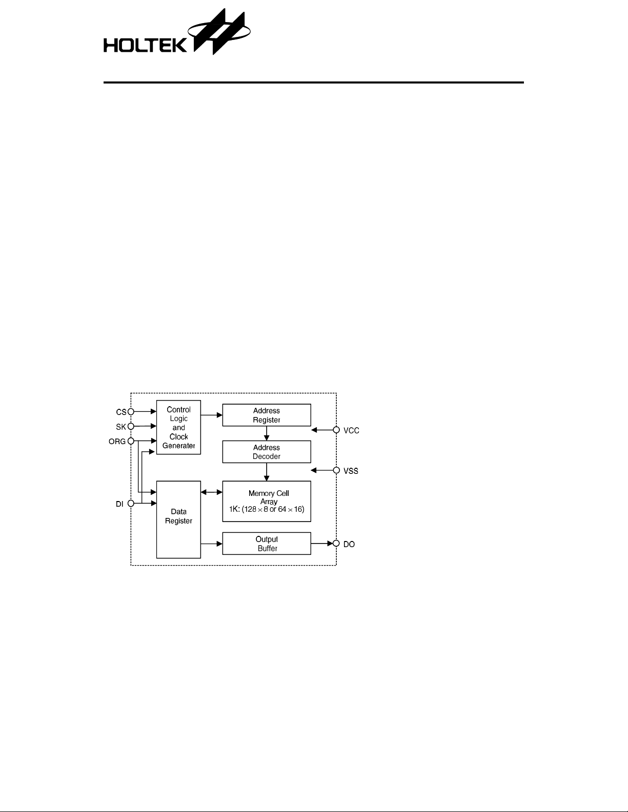
Block Diagram
1 6th May ’99
Page 2
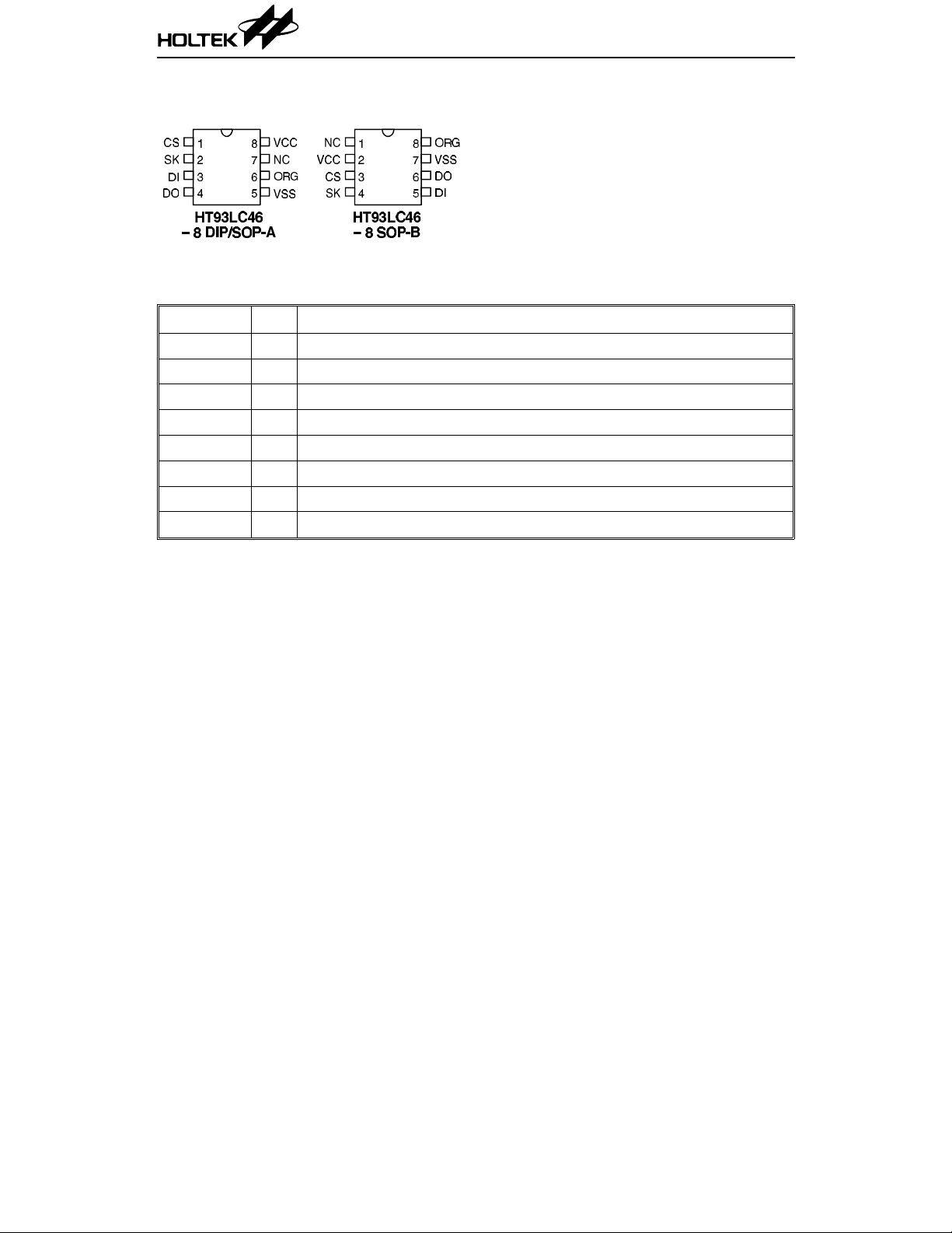
Pin Assignment
Pin Description
Pin Name I/O Description
CS I Chip select input
SK I Serial clock input
DI I Serial data input
DO O Serial data output
VSS I Negative power supply
ORG I Internal Organization
NC — No connection
VCC I Positive power supply
HT93LC46
2 6th May ’99
Page 3
HT93LC46
Absolu te Maxim u m R a tin gs
Operation Temperature (Commercial) ............................................................................ ........0°C to 70°C
Applied V
Applied V oltage on any Pin with Respect to VSS
Supply READ Voltage................................................................................................................ 2V to 5.5V
Note: These are stress ratings o nly. Stresses exceeding the range specified under “Ab solute Ma xi-
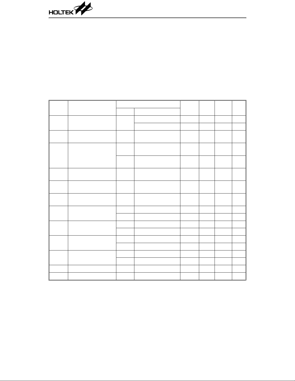
D.C. Characteristics
Voltage with Respect to VSS .............................. .... .... .... .... .... .... .... .... .... .... ....–0.3V to 6.0V
CC
..............................................................VSS
–0.3V to VCC+0.3V
mum Ratings” may cause substantial damage to the device. Functional operation of this
device at other conditions beyond those listed in the specification is not implied and
prolonged exposure to extreme conditions may affect device reliability.
Symbol Parameter
V
CC
I
CC1
I
CC2
I
STB
I
LI
I
LO
V
IL
V
IH
V
OL
V
OH
C
IN
C
OUT
Operating Voltage —
Operating Current
(TTL)
Operating Current
(CMOS)
Standby Current
(CMOS)
Input Leakage
Current
Output Leakage
Current
Input Low Voltage
Input High Voltage
Output Low Voltage
Output High Voltage
Input Capacitance — VIN=0V, f=250kHz — — 5 pF
Output Capacitance — V
Test Conditions
V
CC
Conditions
Min. Typ. Max. Unit
Read 2.0 — 5.5 V
Write 2.4 — 5.5 V
DO unload,
5V
5V
2~5.5V
SK=1MHz
DO unload,
SK=1MHz
DO unload,
SK=250kHz
——5mA
——5mA
——5mA
5V CS=SK=DI=0V — — 10
5V V
5V
IN=VSS~VCC
V
OUT=VSS~VCC
CS=0V
0—1µA
0—1
5V — 0 — 0.8 V
2~5.5V — 0 — 0.1V
5V — 2 — V
2~5.5V — 0.9V
5V I
2~5.5V I
5V I
2~5.5V I
=2.1mA — — 0.4 V
OL
=10µA——0.2V
OL
=–400µA2.4——V
OH
=–10µAV
OH
=0V, f=250kHz — — 5 pF
OUT
CC
–0.2 — — V
—VCCV
CC
CC
CC
µA
µA
V
V
3 6th May ’99
Page 4
A.C. Characteristics
HT93LC46
Symbol Parameter
VCC=5V
±10% VCC=3V±10% VCC=2V*
Min. Max. Min. Max. Min. Max.
f
SK
t
SKH
t
SKL
t
CSS
t
CSH
t
CDS
t
DIS
t
DIH
t
PD1
t
PD0
t
SV
t
HV
t
PR
Clock Frequency 0 2000 0 500 0 250 kHz
SK High Time 250 — 1000 — 2000 — ns
SK Low Time 250 — 1000 — 2000 — ns
CS Setup Time 50 — 200 — 200 — ns
CS Hold Time 0 — 0 — 0 — ns
CS Deselect Time 250 — 250 — 1000 — ns
DI Setup Time 100 — 200 — 400 — ns
DI Hold Time 100 — 200 — 400 — ns
DO Delay to “1” — 250 — 1000 — 2000 ns
DO Delay to “0” — 250 — 1000 — 2000 ns
Status Valid Time — 250 — 250 — — ns
DO Disable Time 100 — 400 — 400 — ns
Write Cycle Time — 2 — 2 — — ms
* For Read Operating Only
A.C. test conditions
Input rise and fall time: 5ns (1V to 2V)
Input and output timing reference levels: 1.5V
Output load: See Figure right
Unit
Output load circuit
4 6th May ’99
Page 5
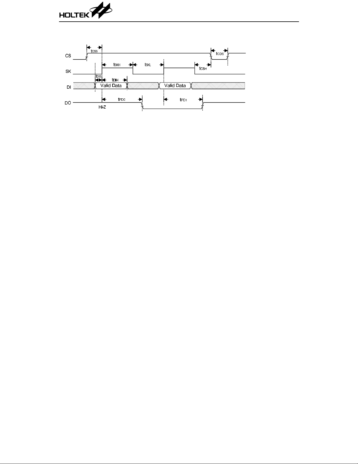
Timing Diagrams
Functional Description
The HT93LC46 is accessed via a three-wire serial
communication interface. The device is arranged
into 64 words by 16 bits or 128 words by 8 bits
depending whether the ORG pin is connected to
VCC or VSS. The HT93LC46 contains seven instructions: READ, ERASE, WRITE, EWEN,
EWDS, ERAL and WRAL. When the user selectable internal organization is arranged
into 64
made up of 9(10) bits data: 1 start bit, 2 op code
bits and 6(7) address bits.
By using the control signal CS, SK and data
input signal DI, these instructions can be given
to the HT93LC46. These serial instruction data
presented at the DI input will be writte n into
the device at the rising edge of SK. During the
READ cycle, DO pin acts as the data output and
during the WRITE or ERASE cycle, DO pin
indicates the BUSY/READY status. When the
DO pin is active for read data or as a
BUSY/READY indicator the CS pin must be
high; otherwise DO pin will be in a high-impedance state. For successful instructions, CS must
be low once a fter the instruction is s ent. After
power on, the device is by default in the EWDS
state. And, an EWEN in structio n mu st be pe rformed before any ERASE or WRITE instruction can be executed. The following are the
functional descrip tio ns an d tim ing dia gram s o f
all seven instructions.
×16 (128×8), these instructions are all
HT93LC46
READ
The READ instruction will stream out data at a
specified addres s on the DO pin. The data on
DO pin changes du ring th e low-to-hi gh edge o f
SK signal. The 8 bits or 16 bits data stream is
preceded by a logi cal “0” dummy bit. Irrespective of the condition of the EWEN or EWDS
instruction, the READ command is always
valid and independent of these two instructions. After the data word has bee n read the
internal address will be automatically incremented by 1 allowing the next consecutive data
word to be read out without entering further
address data. The address will wrap around
with CS High until CS returns to LOW.
EWEN/EWDS
The EWEN/EWDS instruction will enable or
disable the programm ing capabilities. At bo th
the power on and power off state the devi ce automatically entered the disable mode. Before a
WRITE, ERASE, WRAL or ERAL instruction is
given, the programming enable instruction
EWEN must be issued, otherwise the
ERASE/WRITE instruction is invalid. After the
EWEN instruction is issued, the programming
enable condition remains until power is turned off
or a EWDS instruction is given. No data can be
written into the device in the programming disabled state. By so doing, the internal memory
data can be protected.
5 6th May ’99
Page 6

HT93LC46
ERASE
The ERASE instruction erases data at the
specified addresses in the programming enable
mode. After the ERASE op-code and the specified address have been issued, the data erase is
activated by the falling e dge of CS. Since the
internal auto-timing generator provides all timing signals for the internal erase, so the SK
clock is not required. During the internal erase,
we can verify the busy/ready status if CS is
high. The DO pin will remain low but when the
operation is over , the DO pin will return to high
and further instructions can be executed.
WRITE
The WRITE instruction writes data into the
device at the specified addresses in the programming enable mode. After the WRITE opcode and the specified address and data have
been issued, the data writing is activated by the
falling edge of CS. Since the internal auto -timing generator provides all timing signal for the
internal writing, so the SK clock is not required.
The auto-timing write cycl e includes an automatic erase-before-write capability. So, it is not
necessary to erase data before the WRITE instruction. During the internal writing, we can
verify the busy/ready sta tus if CS is high. The
DO pin will remain low but when the operation
is over, the DO pin will return to high and
further instructions can be executed.
ERAL
The ERAL instruction erases the entire 64×16
or 128
×8 memory cells to logical “1” state in the
programming enable mode. After the erase-all
instruction set has be en issued, the data erase
feature is activated by the falling edge of CS.
Since the internal auto-timing generator provides all timing signal for th e erase-all operation, so the SK clock is not required. During the
internal erase-all op eration, we can verify the
busy/ready status if CS is high. The DO pin will
remain low but whe n the o pera tio n is over, the
DO pin will return to high and further ins truction can be executed.
WRAL
The WRAL instruction wri tes data in to the e ntire 64
×16 or 128×8 memory cells in the pro-
gramming enable mode. After the write-all
instruction set has be en issued, the d ata writing is activated by the falling edge of CS. Since
the internal auto-timing generator provi des all
timing signals for the write-all operation, so the
SK clock is not requi red. During the internal
write-all operation, we can verify the
busy/ready status if CS is high. The DO pin will
remain low but wh en the op eration is over the
DO pin will return to high and further ins truction can be executed.
6 6th May ’99
Page 7
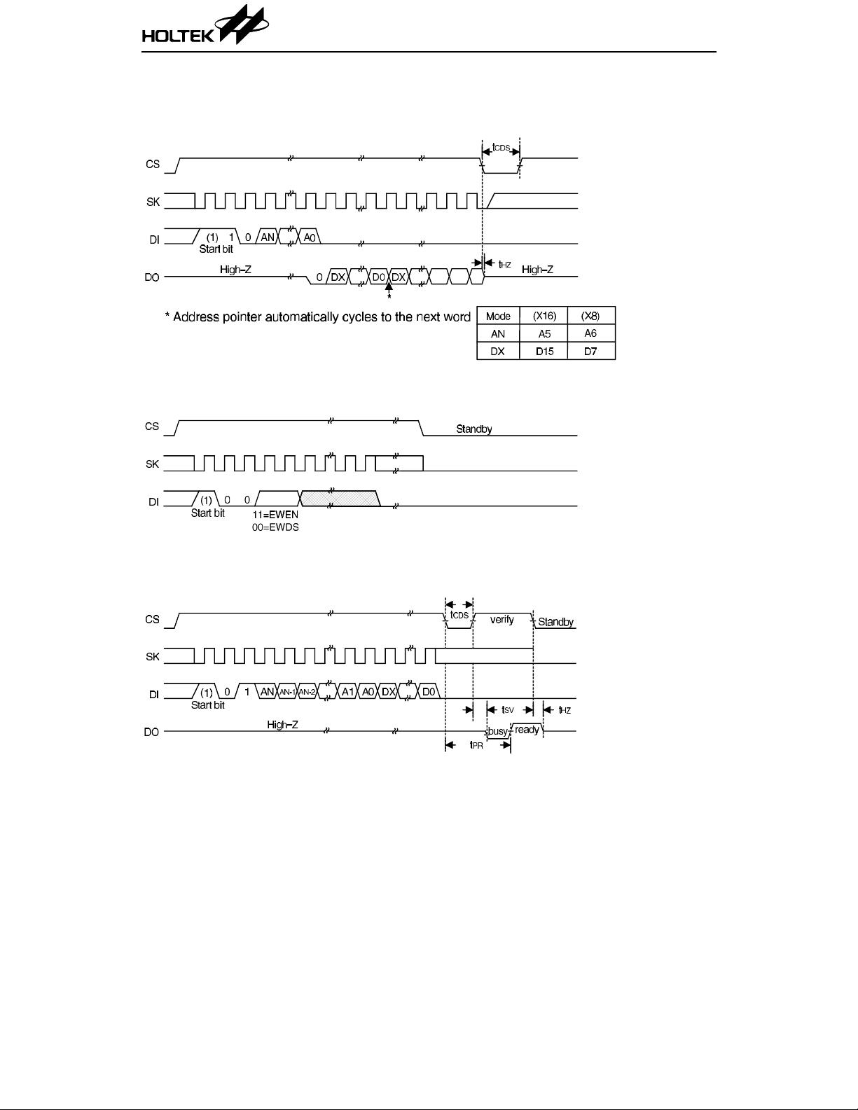
Timing Diagrams
READ
EWEN/EWDS
HT93LC46
WRITE
7 6th May ’99
Page 8

ERASE
ERAL
HT93LC46
WRAL
8 6th May ’99
Page 9

HT93LC46
Instruction Set Summary
HT93LC46
Instruction Comments
READ Read data 1 10 A6~A0 A5~A0 D7~D0 D15~D0
ERASE Erase data 1 11 A6~A0 A5~A0 —
WRITE Write data 1 01 A6~A0 A5~A0 D7~D0 D15~D0
EWEN Erase/Write Enable 1 00 11XXXXX 11XXXX —
EWDS Erase/Write Disable 1 00 00XXXXX 00XXXX —
ERAL Eras e All 1 00 10XXXXX 10XXXX —
WRAL W rite All 1 00 01XXXXX 01XXXX D7~D0 D15~D0
Note: X stands for “don’t care”
Start
bitOpCode
Address
ORG=0 ORG=1
X8 X16
Data
ORG=0 ORG=1
X8 X16
9 6th May ’99
Page 10

Holtek Semiconductor Inc. (Headquarters)
No.3, Creation Rd. II, Science-based Industrial Park, Hsinchu, Taiwan
Tel: 886-3-563-1999
Fax: 886-3-563-1189
Holtek Semiconductor Inc. (Sales Office)
11F, No.576, Sec.7 Chung Hsiao E. Rd., Taipei, Taiwan
Tel: 886-2-2782-9635
Fax: 886-2-2782-9636
Fax: 886-2-2782-7128 (International sales hotline)
Holtek Semiconductor (Shanghai) Inc.
7th Floor, Building 2, No.889, Yi Shan Rd., Shanghai, China
Tel: 021-6485-5560
Fax: 021-6485-0313
Holtek Semiconductor (Hong Kong) Ltd.
RM.711, Tower 2, Cheung Sha Wan Plaza, 833 Cheung Sha Wan Rd., Kowloon, Hong Kong
Tel: 852-2-745-8288
Fax: 852-2-742-8657
Holmate Semiconductor, Inc.
48531 Warm Springs Boulevard, Suite 413, Fremont, CA 94539
Tel: 510-252-9880
Fax: 510-252-9885
HT93LC46
Copyright Ó 1999 by HOLTEK SEMICONDUCTOR INC.
The information appearing in this Data Sheet is believed to be accurate at the time of publication. However, Holtek
assumes no responsibility arising from the use of the specifications described. The applications mentioned herein are
used solely for the purpose of illustration and Holtek makes no warranty or representation that such applications
will be suitable without further modification, nor recommends the use of its products for application that may pres
ent a risk to human life due to malfunction or otherwise. Holtek reserves the right to alter its products without prior
notification. For the most up-to-date information, please visit our web site at http://www.holtek.com.tw.
10 6th May '99
-
 Loading...