

Page 1

Features
·
Operating voltage: 3.0V~5.5V
·
8 input lines
·
16 bidirectional I/O lines
·
Two external interrupt input
·
One 8-bit and one 16-bit programmable timer/event
counter with PFD (programmable frequency divider)
function
·
LCD driver with 41´3or40´4 segments
·
8K´16 program memory EPROM
·
224´8 data memory RAM
·
Real Time Clock (RTC)
·
8-bit prescaler for RTC
General Description
The HT49R70A-1 is an 8-bit high performance single
chip MCU. Its single cycle instruction and two-stage
pipeline architecture make it suitable for high speed ap
plications. The device is also suitable for use in multiple
HT49R70A-1
8-Bit LCD Type OTP MCU
·
Watchdog Timer
·
Buzzer output
·
On-chip crystal, RC and 32768Hz crystal oscillator
·
HALT function and wake-up feature reduce power
consumption
·
8-level subroutine nesting
·
Bit manipulation instruction
·
16-bit table read instruction
·
Up to 0.5ms instruction cycle with 8MHz system clock
·
63 powerful instructions
·
All instructions in 1 or 2 machine cycles
·
100-pin QFP package
LCD low power applications such as scales, leisure
products, high-level household appliances, hand held
LCD products, and battery operated systems in particu
lar.
-
Rev. 1.00 1 December 4, 2001
Page 2
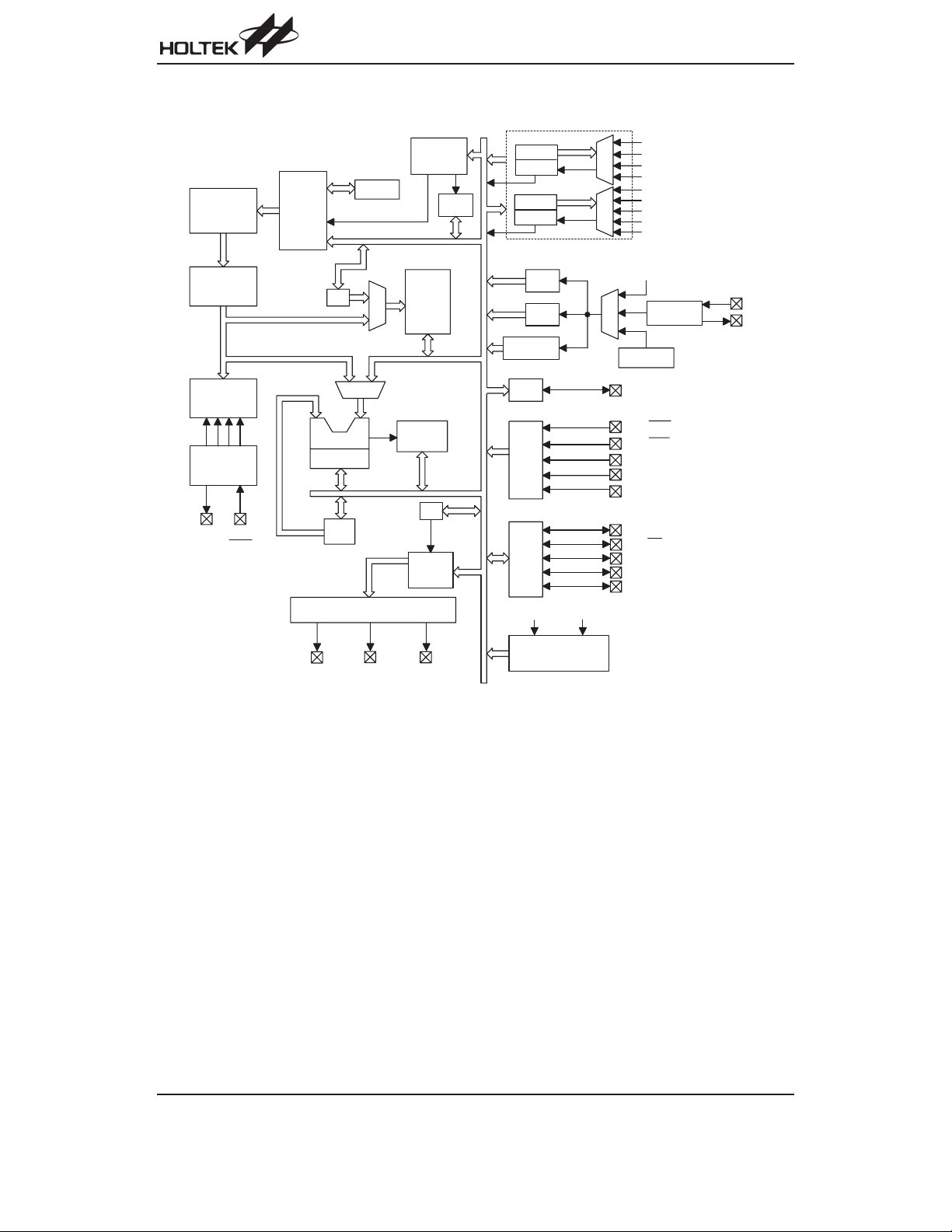
Block Diagram
P r o g r a m
E P R O M
I n s t r u c t i o n
R e g i s t e r
P r o g r a m
C o u n t e r
HT49R70A-1
f
/ 4
M
U
X
W D T O S C
S Y S
f
S Y S
R T C O u t
P B 2 / T M R 0
P B 3 / T M R 1
T M R 0 O V
f
S Y S
T i m e B a s e O u t
f
T 1 D
/ 4
f
S Y S
R T C O S C
O S C 3
O S C 4
S T A C K
I n t e r r u p t
C i r c u i t
I N T C
T M R 0 C
T M R 0
P F D 0
T M R 1 C
T M R 1
P F D 1
M
U
X
M
U
X
R T C
M
M P
D A T A
U
M e m o r y
X
W D T
T i m e B a s e
I n s t r u c t i o n
D e c o d e r
T i m i n g
G e n e r a t i o n
O S C 2
O S C 4
O S C 1
R E S
V D D
V S S
O S C 3
C O M 0 ~
C O M 2
M U X
A L U
S h i f t e r
A C C
L C D D R I V E R
C O M 3 /
S E G 4 0
S T A T U S
L C D
M e m o r y
S E G 0 ~
S E G 3 9
P C
P O R T B
P C 0 ~ P C 7
P B 0 / I N T 0
P B 1 / I N T 1
P B
P B 2 / T M R 0
P B 3 / T M R 1
P B 4 ~ P B 7
B P
P O R T A
P A 0 / B Z
P A 1 / B Z
P A
P A 2
P A 3 / P F D
P A 4 ~ P A 7
E N / D I S
H A L T
L V D / L V R
Rev. 1.00 2 December 4, 2001
Page 3
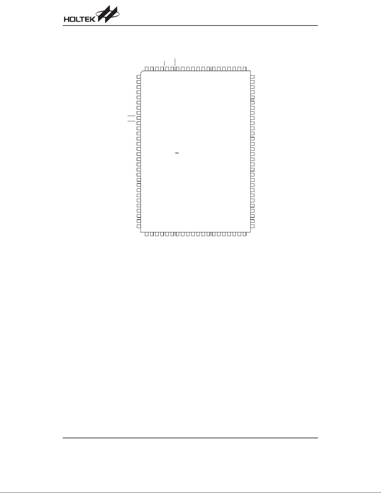
Pin Assignment
HT49R70A-1
P A 3 / P F D
P A 0 / B Z
P A 1 / B Z
O S C 1
P A 4
R E S
P A 2
O S C 4
O S C 3
O S C 2
S E G 0
S E G 1
S E G 2
S E G 3
S E G 4
S E G 5
S E G 6
S E G 7
V D D
S E G 8
P B 0 / I N T 0
P B 1 / I N T 1
P B 2 / T M R 0
P B 3 / T M R 1
V S S
P A 5
P A 6
P A 7
P B 4
P B 5
P B 6
P B 7
P C 0
P C 1
P C 2
P C 3
P C 4
P C 5
P C 6
P C 7
1
2
N C
3
N C
4
N C
5
N C
6
N C
7
8
9
1 0
1 1
1 2
1 3
1 4
1 5
1 6
1 7
1 8
1 9
2 0
2 1
2 2
2 3
2 4
2 5
N C
2 6
N C
2 7
N C
2 8
N C
2 9
N C
3 0
3 1
3 2 3 3 3 4 3 5 3 6 3 7 3 8 3 9 4 0 4 1 4 2 4 3 4 4 4 5 4 6 4 7 4 8 4 9 5 0
V 2
V 1
V L C D
C O M 0
C 2
C 1
H T 4 9 R 7 0 A - 1
1 0 0 Q F P - A
C O M 3 / S E G 4 0
S E G 3 9
C O M 2
C O M 1
S E G 3 8
S E G 3 7
S E G 3 6
S E G 3 5
S E G 3 4
S E G 3 3
8 18 28 38 48 58 68 78 88 99 09 19 29 39 49 59 69 79 89 91 0 0
8 0
S E G 9
7 9
S E G 1 0
7 8
S E G 1 1
7 7
N C
N C
7 6
N C
7 5
S E G 1 2
7 4
7 3
S E G 1 3
7 2
S E G 1 4
S E G 1 5
7 1
S E G 1 6
7 0
S E G 1 7
6 9
S E G 1 8
6 8
S E G 1 9
6 7
S E G 2 0
6 6
S E G 2 1
6 5
S E G 2 2
6 4
S E G 2 3
6 3
S E G 2 4
6 2
S E G 2 5
6 1
S E G 2 6
6 0
S E G 2 7
5 9
S E G 2 8
5 8
S E G 2 9
5 7
N C
5 6
N C
5 5
N C
5 4
N C
5 3
N C
5 2
N C
5 1
S E G 3 2
S E G 3 1
N C
S E G 3 0
Rev. 1.00 3 December 4, 2001
Page 4
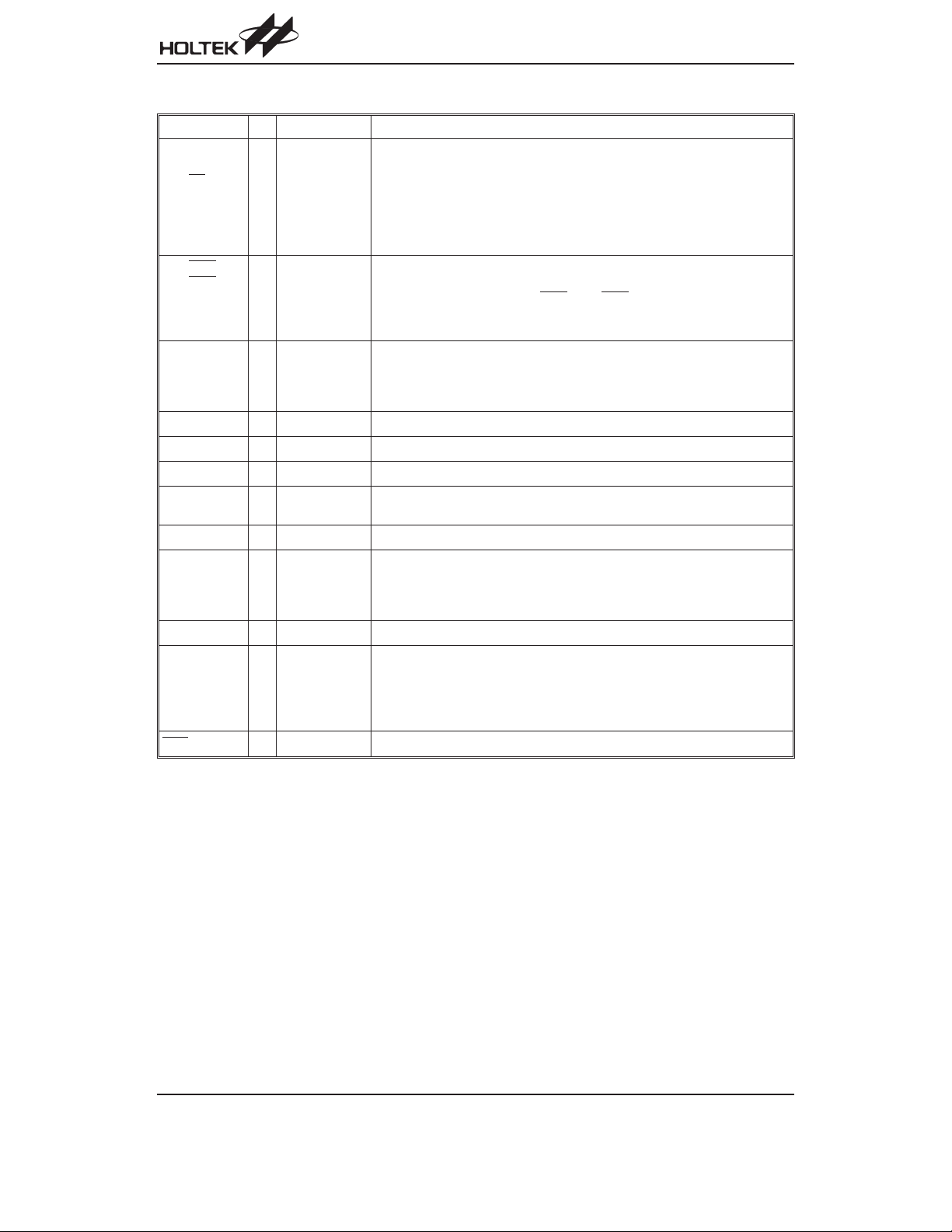
Pin Description
Pin Name I/O Options Description
PA0~PA7 constitute an 8-bit bidirectional input/output port with Schmitt trig
PA0/BZ
PA1/BZ
PA2
PA3/PFD
PA4~PA7
PB0/INT0
PB1/INT1
PB2/TMR0
PB3/TMR1
PB4~PB7
PC0~PC7 I/O
VSS
VLCD I
V1,V2,C1,C2 I
SEG40/COM3
COM2~COM0
SEG39~SEG0 O
OSC4
OSC3
VDD
OSC2
OSC1
RES
I/O
¾¾
O 1/3 or 1/4 Duty
O
¾¾
O
Wake-up
Pull-high
CMOS or
I
Pull-high
CMOS or
I
System Clock
Crystal or RC
I
I
or None
NMOS
¾
or None
NMOS
¾
¾
¾
RTC or
¾
ger input capability. Each bit on port can be configured as a wake-up input by
options. PA0~PA3 can be configured as a CMOS output or NMOS input/out
put with or without pull-high resistor by options. PA4~PA7 are always
pull-high NMOS input/output. Of the eight bits, PA0~PA1 can be set as I/O
pins or buzzer outputs by options. PA3 can be set as an I/O pin or as a PFD
output also by options.
PB0~PB7 constitute an 8-bit Schmitt trigger input port. Each bit on port are
pull-high resistor. Of the eight bits, PB0 and PB1 can be set as input pins or as
external interrupt control pins (INT0
plication. PB2 and PB3 can be set as an input pin or as a timer/event counter
input pin TMR0 and TMR1 also by software application.
PC0~PC7 constitute an 8-bit bidirectional input/output port with a Schmitt trig
ger input capability. On the port, such can be configured as CMOS output or
NMOS input/output with or without pull-high resistor by options.
Negative power supply, ground
LCD power supply
Voltage pump
SEG40 can be set as a segment or as a common output driver for LCD panel
by options. COM2~COM0 are outputs for LCD panel plate.
LCD driver outputs for LCD panel segments
Real time clock oscillators. OSC3 and OSC4 are connected to a 32768Hz
crystal oscillator for timing purposes or to a system clock source (depending
on the options).
No built-in capacitor
Positive power supply
OSC1 and OSC2 are connected to an RC network or a crystal (by options) for
the internal system clock. In the case of RC operation, OSC2 is the output ter-
minal for 1/4 system clock.
The system clock may come from the RTC oscillator. If the system clock co
mes from RTCOSC, these two pins can be floating.
Schmitt trigger reset input, active low
HT49R70A-1
) and (INT1) respectively, by software ap
-
-
-
-
-
Absolute Maximum Ratings
Supply Voltage ...................................VSS-0.3V to 5.5V
Input Voltage..............................V
Note: These are stress ratings only. Stresses exceeding the range specified under ²Absolute Maximum Ratings² may
cause substantial damage to the device. Functional operation of this device at other conditions beyond those
listed in the specification is not implied and prolonged exposure to extreme conditions may affect device reliabil
ity.
Rev. 1.00 4 December 4, 2001
-0.3V to VDD+0.3V
SS
Storage Temperature ............................-50°Cto125°C
Operating Temperature...........................-40°Cto85°C
-
Page 5
HT49R70A-1
D.C. Characteristics
Symbol Parameter
V
DD
I
DD1
I
DD2
I
DD3
I
STB1
I
STB2
I
STB3
I
STB4
I
STB5
I
STB6
I
STB7
V
IL1
V
IH1
V
IL2
V
IH2
I
OL
I
OH
R
PH
V
LVR
V
LVD
Note:
Operating Voltage
Operating Current (Crystal OSC)
Operating Current (RC OSC)
Operating Current (f
Standby Current (*fS=T1)
Standby Current (*fS=32.768kHz OSC)
Standby Current (*fS=WDT RC OSC)
Standby Current (*fS=32.768kHz OSC)
Standby Current (*fS=32.768kHz OSC)
Standby Current (*fS=WDT RC OSC)
Standby Current (*fS=WDT RC OSC)
Input Low Voltage for I/O Ports,
TMR and INT
Input High Voltage for I/O Ports,
TMR and INT
Input Low Voltage (RES)
Input High Voltage (RES)
I/O Port Sink Current
I/O Port Source Current
Pull-high Resistance of I/O Ports and
INT0
, INT1
Low Voltage Reset Voltage
Low Voltage Detector Voltage
² please refer to clock option of WDT (page 12)
²*f
S
=32768Hz)
SYS
Test Conditions
V
DD
Conditions
¾¾
3V
No load, f
5V
3V
No load, f
5V
3V
No load
5V
3V
No load, system HALT
LCD off at HALT
5V
3V
No load, system HALT
LCD on at HALT, C type
5V
3V
No load, system HALT
LCD on at HALT, C type
5V
No load, system HALT
3V
LCD on at HALT
5V
R type, 1/2bias
No load, system HALT
3V
LCD on at HALT
5V
R type, 1/3bias
No load, system HALT
3V
LCD on at HALT
5V
R type, 1/2bias
No load, system HALT
3V
LCD on at HALT
5V
R type, 1/3bias
3V
5V
3V
5V
3V
5V
3V
5V
=0.1V
V
3V
OL
=0.1V
V
5V
OL
=0.9V
V
3V
OH
V
OH
=0.9V
5V
3V
5V
LVD voltage 3.3V option 2.7 3.2 3.6 V
¾
LVD voltage 3.3V option 3.0 3.3 3.6 V
¾
SYS
SYS
DD
DD
DD
DD
=4MHz
=4MHz
¾
¾
¾
¾
¾
¾
¾
¾
¾
¾
Min. Typ. Max. Unit
3.0
¾
2.0 3.0 mA
¾
5.0 8.0 mA
¾
1.8 2.7 mA
¾
4.6 7.5 mA
¾
1.2 2 mA
¾
¾
47mA
¾¾
¾¾
¾4
¾14
¾
¾
¾
¾
¾
¾
¾
¾
¾
¾
0
0
0.8V
0.8V
0
0
0.9V
0.9V
25
610
17 30
34 60
13 25
28 50
14 25
26 50
10 20
19 40
¾
¾
¾
DD
¾
DD
¾
¾
¾
DD
¾
DD
0.2V
0.2V
0.4V
0.4V
612
10 25
-2 -4 ¾
-5 -8 ¾
40 60 80
10 30 50
Ta=25°C
5.5 V
1
2
10
20
DD
DD
V
DD
V
DD
DD
DD
V
DD
V
DD
¾
¾
mA
mA
mA
mA
mA
mA
mA
mA
mA
mA
mA
mA
mA
mA
V
V
V
V
V
V
V
V
mA
mA
mA
mA
kW
kW
Rev. 1.00 5 December 4, 2001
Page 6

HT49R70A-1
A.C. Characteristics
Symbol Parameter
f
SYS1
f
SYS2
f
SYS3
f
RTCOSC
f
TIMER
t
WDTOSC
t
RES
t
SST
t
INT
Note: t
System Clock (Crystal OSC)
System Clock (RC OSC)
System Clock (32768Hz Crystal OSC)
RTC Frequency
Timer I/P Frequency (TMR0/TMR1)
Watchdog Oscillator
External Reset Low Pulse Width
System Start-up Timer Period
Interrupt Pulse Width
= 1/f
SYS
SYS
Test Conditions
V
DD
3V
5V
3V
5V
Conditions
¾
¾
¾
¾
¾¾ ¾
¾¾ ¾
3V
5V
3V
5V
¾
¾
¾
¾
¾¾
Power-up or wake-up
¾
from HALT
¾¾
Min. Typ. Max. Unit
400
400
400
400
¾
¾
¾
¾
32768
32768
0
¾
0
¾
45 90 180
35 65 130
1
¾¾ms
1024
¾
1
¾¾ms
Ta=25°C
4000 kHz
8000 kHz
4000 kHz
8000 kHz
Hz
¾
Hz
¾
4000 kHz
8000 kHz
ms
ms
t
¾
SYS
Rev. 1.00 6 December 4, 2001
Page 7
Functional Description
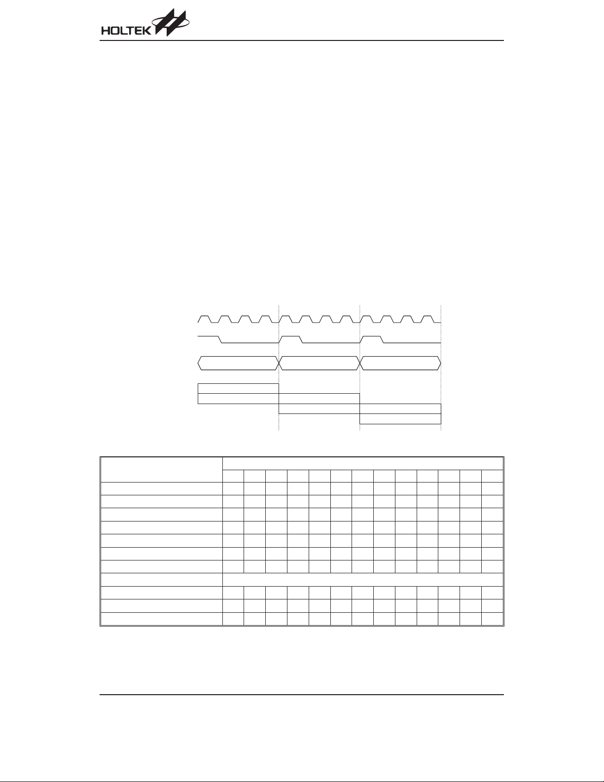
Execution flow
The system clock is derived from either a crystal or an
RC oscillator or a 32768Hz crystal oscillator. It is inter
nally divided into four non-overlapping clocks. One in
struction cycle consists of four system clock cycles.
Instruction fetching and execution are pipelined in such
a way that a fetch takes one instruction cycle while de
coding and execution takes the next instruction cycle.
The pipelining scheme makes it possible for each in
struction to be effectively executed in a cycle. If an in
struction changes the value of the program counter, two
cycles are required to complete the instruction.
Program counter - PC
The program counter (PC) is 13 bits wide and it controls
the sequence in which the instructions stored in the pro
gram ROM are executed. The contents of the PC can
specify a maximum of 8192 addresses.
HT49R70A-1
After accessing a program memory word to fetch an in
struction code, the value of the PC is incremented by 1.
The PC then points to the memory word containing the
next instruction code.
-
When executing a jump instruction, conditional skip ex
ecution, loading a PCL register, a subroutine call, an ini
tial reset, an internal interrupt, an external interrupt, or
returning from a subroutine, the PC manipulates the
program transfer by loading the address corresponding
to each instruction.
-
The conditional skip is activated by instructions. Once
the condition is met, the next instruction, fetched during
the current instruction execution, is discarded and a
dummy cycle replaces it to get a proper instruction; oth
erwise proceed to the next instruction.
The lower byte of the PC (PCL) is a readable and
writeable register (06H). Moving data into the PCL per
forms a short jump. The destination is within 256 loca
tions.
-
-
-
-
-
-
S y s t e m C l o c k
O S C 2 ( R C o n l y )
T 1 T 2 T 3 T 4 T 1 T 2 T 3 T 4 T 1 T 2 T 3 T 4
P C
P C P C + 1 P C + 2
F e t c h I N S T ( P C )
E x e c u t e I N S T ( P C - 1 )
F e t c h I N S T ( P C + 1 )
E x e c u t e I N S T ( P C )
F e t c h I N S T ( P C + 2 )
E x e c u t e I N S T ( P C + 1 )
Execution flow
Mode
*12 *11 *10 *9 *8 *7 *6 *5 *4 *3 *2 *1 *0
Program Counter
Initial Reset 0000000000000
External Interrupt 0 0000000000100
External Interrupt 1 0000000001000
Timer/Event Counter 0 overflow 0000000001100
Timer/Event Counter 1 overflow 0000000010000
Time Base Interrupt 0000000010100
RTC Interrupt 0000000011000
Skip PC+2
Loading PCL *12 *11 *10 *9 *8 @7 @6 @5 @4 @3 @2 @1 @0
Jump, Call Branch #12 #11 #10 #9 #8 #7 #6 #5 #4 #3 #2 #1 #0
Return From Subroutine S12 S11 S10 S9 S8 S7 S6 S5 S4 S3 S2 S1 S0
Program counter
Note: *12~*0: Program counter bits S12~S0: Stack register bits
#12~#0: Instruction code bits @7~@0: PCL bits
Rev. 1.00 7 December 4, 2001
Page 8

When a control transfer takes place, an additional
dummy cycle is required.
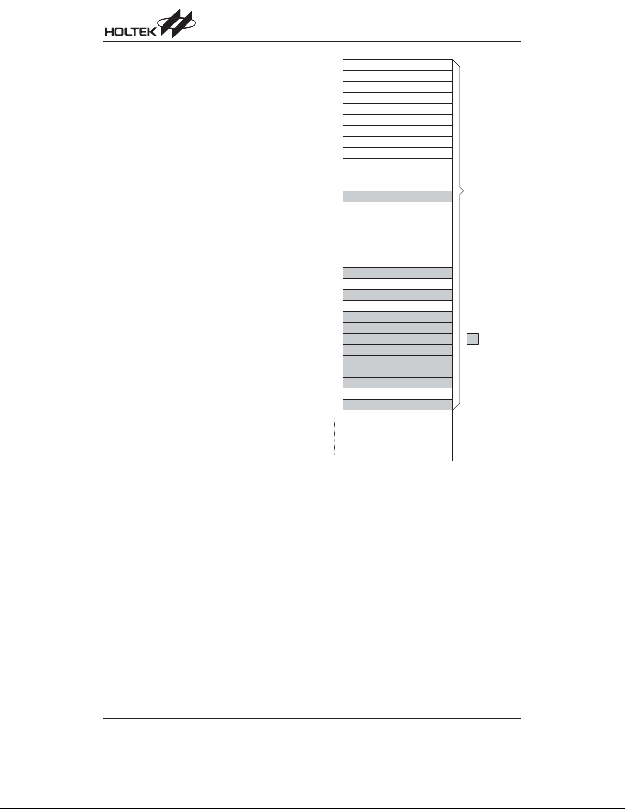
Program memory - EPROM
The program memory (EPROM) is used to store the pro
gram instructions which are to be executed. It also con
tains data, table, and interrupt entries, and is organized
into 8192´16 bits which are addressed by the PC and
table pointer.
Certain locations in the ROM are reserved for special
usage:
·
Location 000H
Location 000H is reserved for program initialization.
After chip reset, the program always begins execution
at this location.
·
Location 004H
Location 004H is reserved for the external interrupt
service program. If the INT0
input pin is activated, and
the interrupt is enabled, and the stack is not full, the
program begins execution at location 004H.
0 0 0 H
0 0 4 H
0 0 8 H
0 0 C H
0 1 0 H
0 1 4 H
0 1 8 H
n 0 0 H
n F F H
1 F F F H
D e v i c e i n i t i a l i z a t i o n p r o g r a m
E x t e r n a l i n t e r r u p t 0 s u b r o u t i n e
E x t e r n a l i n t e r r u p t 1 s u b r o u t i n e
T i m e r / e v e n t c o u n t e r 0 i n t e r r u p t s u b r o u t i n e
T i m e r / e v e n t c o u n t e r 1 i n t e r r u p t s u b r o u t i n e
T i m e B a s e I n t e r r u p t
R T C I n t e r r u p t
L o o k - u p t a b l e ( 2 5 6 w o r d s )
L o o k - u p t a b l e ( 2 5 6 w o r d s )
1 6 b i t s
N o t e : n r a n g e s f r o m 0 t o 1 F
P r o g r a m
R O M
Program memory
HT49R70A-1
·
Location 008H
Location 008H is reserved for the external interrupt
service programalso. If the INT1
and the interrupt is enabled, and the stack is not full,
-
-
the program begins execution at location 008H.
·
Location 00CH
Location 00CH is reserved for the Timer/Event Coun
ter 0 interrupt service program. If a timer interrupt re
sults from a Timer/Event Counter 0 overflow, and if the
interrupt is enabled and the stack is not full, the pro
gram begins execution at location 00CH.
·
Location 010H
Location 010H is reserved for the Timer/Event Coun
ter 1 interrupt service program. If a timer interrupt re
sults from a Timer/Event Counter 1 overflow, and if the
interrupt is enabled and the stack is not full, the pro
gram begins execution at location 010H.
·
Location 014H
Location 014H is reserved for the Time Base interrupt
service program. If a Time Base interrupt occurs, and
the interrupt is enabled, and the stack is not full, the
program begins execution at location 014H.
·
Location 018H
Location 018H is reserved for the real time clock inter
rupt service program. If a real time clock interrupt occurs, and the interrupt is enabled, and the stack is not
full, the program begins execution at location 018H.
·
Table location
Any location in the ROM can be used as a look-up table. The instructions ²TABRDC [m]² (the current page,
1 page=256 words) and ²TABRDL [m]² (the last page)
transfer the contents of the lower-order byte to the
specified data memory, and the contents of the
higher-order byte to TBLH (Table Higher-order byte
register) (08H). Only the destination of the lower-order
byte in the table is well-defined; the other bits of the ta
ble word are all transferred to the lower portion of
TBLH. The TBLH is read only, and the table pointer
(TBLP) is a read/write register (07H), indicating the ta
ble location. Before accessing the table, the location
should be placed in TBLP. All the table related instruc
tions require 2 cycles to complete the operation.
These areas may function as a normal ROM depend
ing upon the user's requirements.
input pinis activated,
-
-
-
-
-
-
-
-
-
-
-
Instruction(s)
*12 *11 *10 *9 *8 *7 *6 *5 *4 *3 *2 *1 *0
Table Location
TABRDC [m] P12 P11 P10 P9 P8 @7 @6 @5 @4 @3 @2 @1 @0
TABRDL [m] 1 1 1 1 1 @7 @6 @5 @4 @3 @2 @1 @0
Table location
Note: *12~*0: Table location bits P12~P8: Current program counter bits
@7~@0: Table pointer bits
Rev. 1.00 8 December 4, 2001
Page 9
HT49R70A-1
Stack register - STACK
The stack register is a special part of the memory used
to save the contents of the PC. The stack is organized
into 8 levels and is neither part of the data nor part of the
program, and is neither readable nor writeable. Its acti
vated level is indexed by a stack pointer (SP) and is nei
ther readable nor writeable. At the start of a subroutine
call or an interrupt acknowledgment, the contents of the
PC is pushed onto the stack. At the end of the subrou
tine or interrupt routine, signaled by a return instruction
(RET or ), the contents of the PC is restored to its previ
ous value from the stack. After chip reset, the SP will
point to the top of the stack.
If the stack is full and a non-masked interrupt takes
place, the interrupt request flag is recorded but the ac
knowledgment is still inhibited. Once the SP is decre
mented (by RET or RETI), the interrupt is serviced. This
feature prevents stack overflow, allowing the program
mer to use the structure easily. Likewise, if the stack is
full, and a ²CALL² is subsequently executed, a stack
overflow occurs and the first entry is lost (only the most
recent six return addresses are stored).
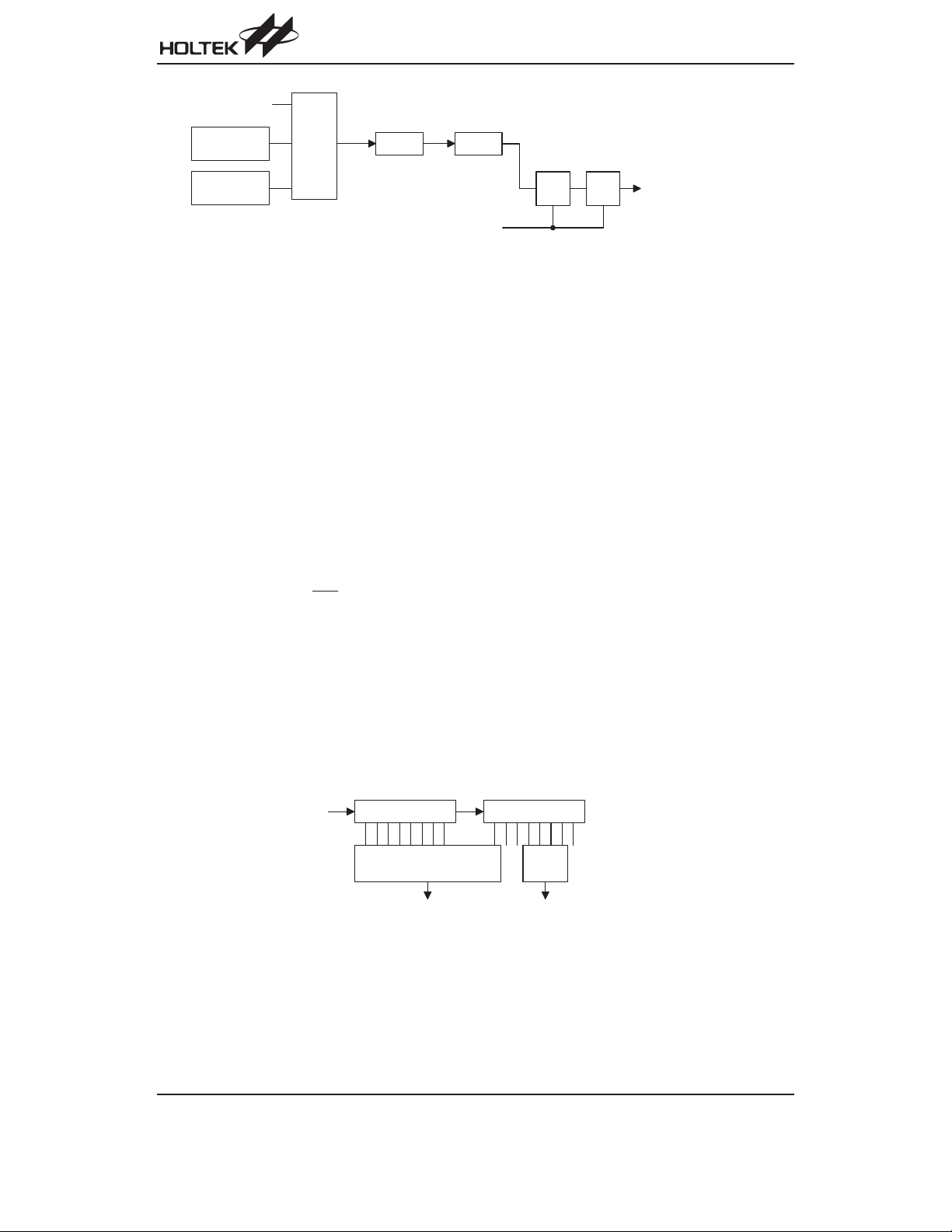
Data memory - RAM
The data memory (RAM) is designed with 245´8 bits,
and is divided into two functional groups, namely; special function registers and general purpose data memory, most of which are readable/writeable, although
some are read only.
Of the two types of functional groups, the special function registers consist of an Indirect addressing register 0
(00H), a Memory pointer register 0 (MP0;01H), an Indirect addressing register 1 (02H), a Memory pointer register 1 (MP1;03H), a Bank pointer (BP;04H), an
Accumulator (ACC;05H), a Program counter
lower-order byte register (PCL;06H), a Table pointer
(TBLP;07H), a Table higher-order byte register
(TBLH;08H), a Real time clock control register
(RTCC;09H), a Status register (STATUS;0AH), an Inter
rupt control register 0 (INTC0;0BH), a Timer/Event
Counter 0 (TMR0;0DH), a Timer/Event Counter 0 con
trol register (TMR0C;0EH), a Timer/Event Counter 1
(TMR1H:0FH;TMR1L:10H), a Timer/Event Counter 1
control register (TMR1C; 11H), I/O registers (PA;12H,
PB;14H, PC;16H), and Interrupt control register 1
(INTC1;1EH). On the other hand, the general purpose
data memory, addressed from 20H to FFH, is used for
data and control information under instruction com
mands.
The areas in the RAM can directly handle arithmetic,
logic, increment, decrement, and rotate operations. Ex
cept some dedicated bits, each bit in the RAM can be
set and reset by ²SET [m].i² and ²CLR [m].i² They are
also indirectly accessible through the Memory pointer
register 0 (MP0;01H) or the Memory pointer register 1
(MP1;03H).
I n d i r e c t A d d r e s s i n g R e g i s t e r 0
0 0 H
0 1 H
I n d i r e c t A d d r e s s i n g R e g i s t e r 1
0 2 H
0 3 H
0 4 H
-
0 5 H
-
0 6 H
0 7 H
0 8 H
-
0 9 H
0 A H
-
0 B H
0 C H
0 D H
0 E H
-
0 F H
-
1 0 H
1 1 H
-
1 2 H
1 3 H
1 4 H
1 5 H
1 6 H
1 7 H
1 8 H
1 9 H
1 A H
1 B H
1 C H
1 D H
1 E H
1 F H
2 0 H
F F H
M P 0
M P 1
B P
A C C
P C L
T B L P
T B L H
R T C C
S T A T U S
I N T C 0
T M R 0
T M R 0 C
T M R 1 H
T M R 1 L
T M R 1 C
P A
P B
P C
I N T C 1
G e n e r a l P u r p o s e
D A T A M E M O R Y
( 2 2 4 B y t e s )
RAM mapping
Indirect addressing register
Location 00H and 02H are indirect addressing registers
that are not physically implemented. Any read/write op
eration of [00H] and [02H] accesses the RAM pointed to
by MP0 (01H) and MP1(03H) respectively. Reading lo
cation 00H or 02H indirectly returns the result 00H.
While, writing it indirectly leads to no operation.
The function of data movement between two indirect ad
dressing registers is not supported. The memory pointer
-
registers, MP0andMP1,are both 8-bit registers used to
access the RAM by combining corresponding indirect
addressing registers. MP0 can only be applied to data
memory, while MP1 can be applied to data memory and
LCD display memory.
S p e c i a l P u r p o s e
D A T A M E M O R Y
: U n u s e d .
R e a d a s " 0 "
-
-
-
Rev. 1.00 9 December 4, 2001
Page 10

HT49R70A-1
Accumulator - ACC
The accumulator (ACC) is related to the ALU opera
tions. It is also mapped to location 05H of the RAM and
is capable of operating with immediate data. The data
movement between two data memory locations must
pass through the ACC.
Arithmetic and logic unit - ALU
This circuit performs 8-bit arithmetic and logic opera
tions and provides the following functions:
·
Arithmetic operations (ADD, ADC, SUB, SBC, DAA)
·
Logic operations (AND, OR, XOR, CPL)
·
Rotation (RL, RR, RLC, RRC)
·
Increment and Decrement (INC, DEC)
·
Branch decision (SZ, SNZ, SIZ, SDZ etc.)
The ALU not only saves the results of a data operation
but also changes the status register.
Status register - STATUS
The status register (0AH) is 8 bits wide and contains, a
carry flag (C), an auxiliary carry flag (AC), a zero flag (Z),
an overflow flag (OV), a power down flag (PD), and a
watchdog time-out flag (TO). It also records the status
information and controls the operation sequence.
Except for the TO and PD flags, bits in the status register can be altered by instructions similar to other registers. Data written into the status register does not alter
the TO or PD flags. Operations related to the status register, however, may yield different results from those intended. The TO and PD flags can only be changed by a
Watchdog Timer overflow, chip power-up, or clearing
the Watchdog Timer and executing the ²HALT² instruction. The Z, OV, AC, and C flags reflect the status of the
latest operations.
On entering the interrupt sequence or executing the
subroutine call, the status register will not be automati
cally pushed onto the stack. If the contents of the status
is important, and if the subroutine is likely to corrupt the
status register, the programmer should take precautions
and save it properly.
Interrupts
The HT49R70A-1 provides two external interrupts, two
internal timer/event counter interrupts, an internal time
base interrupt, and an internal real time clock interrupt.
The interrupt control register 0 (INTC0;0BH) and inter
rupt control register 1 (INTC1;1EH) both contain the in
terrupt control bits that are used to set the
enable/disable status and interrupt request flags.
Once an interrupt subroutine is serviced, other inter
rupts are all blocked (by clearing the EMI bit). This
scheme may prevent any further interrupt nesting.
Other interrupt requests may take place during this in
terval, but only the interrupt request flag will be re
corded. If a certain interrupt requires servicing within the
service routine, the EMI bit and the corresponding bit of
the INTC0 or of INTC1 may be set in order to allow in
terrupt nesting. Once the stack is full, the interrupt re
quest will not be acknowledged, even if the related
interrupt is enabled, until the SP is decremented. If immediate service is desired, the stack should be prevented from becoming full.
All these interrupts can support a wake-up function. As
an interrupt is serviced, a control transfer occurs by
pushing the contents of the PC onto the stack followed
by a branch to a subroutine at the specified location in
the ROM. Only the contents of the PC is pushed onto
the stack. If the contents of the register or of the status
register (STATUS) is altered by the interrupt service pro
-
-
-
-
-
-
-
-
-
Labels Bits Function
C is set if the operation results in a carry during an addition operation or if a borrow does not
C0
take place during a subtraction operation; otherwise C is cleared. C is also affected by a rotate
through carry instruction.
AC 1
AC is set if the operation results in a carry out of the low nibbles in addition or no borrow from
the high nibble into the low nibble in subtraction; otherwise AC is cleared.
Z 2 Z is set if the result of an arithmetic or logic operation is zero; otherwise Z is cleared.
OV 3
PD 4
TO 5
¾
¾
OV is set if the operation results in a carry into the highest-order bit but not a carry out of the
highest-order bit, or vice versa; otherwise OV is cleared.
PD is cleared by either a system power-up or executing the ²CLR WDT² instruction. PD is set
by executing the ²HALT² instruction.
TO is cleared by a system power-up or executing the ²CLR WDT² or ²HALT² instruction. TO is
set by a WDT time-out.
6
Unused bit, read as ²0²
7
Unused bit, read as ²0²
Status register
Rev. 1.00 10 December 4, 2001
Page 11

HT49R70A-1
gram which corrupts the desired control sequence, the
contents should be saved in advance.
External interrupts are triggered by a high to low transi
tion of INT0
flag (EIF0; bit 4 of INTC0, EIF1; bit 5 of INTC0) is set as
well. After the interrupt is enabled, the stack is not full,
and the external interrupt is active, a subroutine call to
location 04H or 08H occurs. The interrupt request flag
(EIF0 or EIF1) and EMI bits are all cleared to disable
other interrupts.
The internal Timer/Event Counter 0 interrupt is initial
ized by setting the Timer/Event Counter 0 interrupt re
quest flag (T0F; bit 6 of INTC0), which is normally
caused by a timer overflow. After the interrupt is en
abled, and the stack is not full, and the T0F bit is set, a
subroutine calltolocation 0CH occurs. The related inter
rupt request flag (T0F) is reset, and the EMI bit is
cleared to disable further interrupts. The Timer/Event
Counter 1 is operated in the same manner but its related
interrupt request flag is T1F (bit 4 of INTC1) and its sub
routine call location is 10H.
The time base interrupt is initialized by setting the time
base interrupt request flag (TBF; bit 5 of INTC1), that is
caused by a regular time base signal. After the interrupt
is enabled, and the stack is not full, and the TBF bit is
set, a subroutine call to location 14H occurs. The related
interrupt request flag (TBF) is reset and the EMI bit is
cleared to disable further interrupts.
The real time clock interrupt is initialized by setting the
real time clock interrupt request flag (RTF; bit 6 of
or INT1, and the related interrupt request
INTC1), that is caused by a regular real time clock sig
nal. After the interrupt is enabled, and the stack is not
full, and the RTF bit is set, a subroutine call to location
18H occurs. The related interrupt request flag (RTF) is
reset and the EMI bit is cleared to disable further inter
rupts.
During the execution of an interrupt subroutine, other in
terrupt acknowledgments are all held until the ²RETI²
instruction is executed or the EMI bit and the related in
terrupt control bit are set both to 1 (if the stack is not full).
To return from the interrupt subroutine, ²RET² or ²RETI²
may be invoked. RETI sets the EMI bit and enables an
interrupt service, but RET does not.
-
Interrupts occurring in the interval between the rising
edges of two consecutive T2 pulses are serviced on the
-
latter of the two T2 pulses if the corresponding interrupts
are enabled. In the case of simultaneous requests, the
priorities in the following table apply. These can be
masked by resetting the EMI bit.
-
No. Interrupt Source Priority Vector
a External interrupt 0 1 04H
b External interrupt 1 2 08H
c Timer/Event Counter0overflow 3 0CH
d Timer/Event Counter 1 overflow 4 10H
e Time base interrupt 5 14H
f Real time clock interrupt 6 18H
-
-
-
-
Register Bit No. Label Function
0 EMI Control the master (global) interrupt (1=enabled; 0=disabled)
1 EEI0 Control the external interrupt 0 (1=enabled; 0=disabled)
2 EEI1 Control the external interrupt 1 (1=enabled; 0=disabled)
INTC0
(0BH)
INTC1
(1EH)
Rev. 1.00 11 December 4, 2001
3 ET0I Control the Timer/Event Counter 0 interrupt (1=enabled; 0=disabled)
4 EIF0 External interrupt 0 request flag (1=active; 0=inactive)
5 EIF1 External interrupt 1 request flag (1=active; 0=inactive)
6 T0F Internal Timer/Event Counter 0 request flag (1=active; 0=inactive)
7
0 ET1I Control the Timer/Event Counter 1 interrupt (1=enabled; 0=disabled)
1 ETBI Control the time base interrupt (1=enabled; 0:disabled)
2 ERTI Control the real time clock interrupt (1=enabled; 0:disabled)
3
4 T1F Internal Timer/Event Counter 1 request flag (1=active; 0=inactive)
5 TBF Time base request flag (1=active; 0=inactive)
6 RTF Real time clock request flag (1=active; 0=inactive)
7
¾ Unused bit, read as ²0²
¾ Unused bit, read as ²0²
¾ Unused bit, read as ²0²
INTC register
Page 12

HT49R70A-1
The Timer/Event Counter 0 interrupt request flag (T0F),
external interrupt 1 request flag (EIF1), external inter
rupt 0 request flag (EIF0), enable Timer/Event Counter
0 interrupt bit (ET0I), enable external interrupt 1 bit
(EEI1), enable external interrupt 0 bit (EEI0), and en
able master interrupt bit (EMI) make up of the Interrupt
Control register 0 (INTC0) which is located at 0BH in the
RAM. The real time clock interrupt request flag (RTF),
time base interrupt request flag (TBF), Timer/Event
Counter 1 interrupt request flag (T1F), enable real time
clock interrupt bit (ERTI), and enable time base interrupt
bit (ETBI), enable Timer/Event Counter 1 interrupt bit
(ET1I) on the other hand, constitute the Interrupt Control
register 1 (INTC1) which is located at 1EH in the RAM.
EMI, EEI0, EEI1, ET0I, ET1I, ETBI, and ERTI are all
used to control the enable/disable status of interrupts.
These bits prevent the requested interrupt from being
serviced. Once the interrupt request flags (RTF, TBF, T0F,
T1F, EIF1, EIF0) are all set, they remain in the INTC1 or
INTC0 respectively until the interrupts are serviced or
cleared by a software instruction.
It is recommended that a program should not use the
²CALL subroutine²within the interrupt subroutine. It¢sbe
cause interrupts often occur in an unpredictable manner
or require to be serviced immediately in some applica
tions. During that period, if only one stack is left, and enabling theinterruptisnotwellcontrolled,operationofthe
²call² in the interrupt subroutine may damage the original control sequence.
Oscillator configuration
The HT49R70A-1 provides three oscillator circuits for
system clocks, i.e., RC oscillator, crystal oscillator and
32768Hz crystal oscillator, determined by options. No
matter what type of oscillator is selected, the signal is
used for the system clock. The HALT mode stops the
system oscillator (RC and crystal oscillator only) and ig
nores external signal in order to conserve power. The
32768Hz crystal oscillator (system oscillator) still runs at
HALT mode. If the 32768Hz crystal oscillator is selected
as the system oscillator, the system oscillator is not
stopped; but the instruction execution is stopped. Since
the system oscillator or oscillator) is also designed for
timing purposes, the internal timing (RTC, time base,
WDT) operation still runs even if the system enters the
HALT mode.
Of the three oscillators, if the RC oscillator is used, an
external resistor between OSC1 and VSS is required,
and the range of the resistance should be from 40kW to
680kW. The system clock, divided by 4, is available on
-
OSC2 with pull-high resistor, which can be used to syn
chronize external logic. The RC oscillator provides the
most cost effective solution. However, the frequency of
the oscillation may vary with VDD, temperature, and the
chip itself due to process variations. It is therefore, not
suitable for timing sensitive operations where accurate
oscillator frequency is desired.
On the other hand, if the crystal oscillator is selected, a
crystal across OSC1 and OSC2 is needed to provide
the feedback and phase shift required for the oscillator,
and no other external components are required. A reso
nator may be connected between OSC1 and OSC2 to
replace the crystal and to get a frequency reference, but
two external capacitors in OSC1 and OSC2 are re
quired.
There is another oscillator circuit designed for the real
time clock. In this case, only the 32.768kHz crystal oscil
lator can be applied. The crystal should be connected
between OSC3 and OSC4.
The RTC oscillator circuit can be controlled to oscillate
quickly by setting the ²QOSC² bit (bit 4 of RTCC). It is
recommended to turn on the quick oscillating function
upon power on, and then turn it off after 2 seconds.
The WDT oscillator is a free running on-chip RC oscillator, and no external components are required. Although
the system enters the power down mode, the system
clock stops, and the WDT oscillator still works with a period of approximately 78ms. The WDT oscillator can be
disabled by options to conserve power.
Watchdog Timer - WDT
The WDT clock source is implemented by a dedicated
RC oscillator (WDT oscillator) or an instruction clock
(system clock/4) or a real time clock oscillator (RTC os
cillator). The timer is designed to prevent a software
malfunction or sequence from jumping to an unknown
location with unpredictable results. The WDT can be
disabled by options. But if the WDT is disabled, all exe
cutions related to the WDT lead to no operation.
-
-
-
-
-
-
O S C 3
O S C 4
3 2 7 6 8 H z C r y s t a l / R T C O s c i l l a t o r
O S C 1
/ 4
f
O S C 2
C r y s t a l O s c i l l a t o r R C O s c i l l a t o r
S Y S
O S C 1
V
D D
O S C 2
System oscillator
Rev. 1.00 12 December 4, 2001
Page 13
S y s t e m C l o c k / 4
HT49R70A-1
R T C
O S C
W D T
O S C
3 2 7 6 8 H z
1 2 k H z
R O M
C o d e
O p t i o n
f
S
D i v i d e r
W D T C l e a r
Watchdog Timer
The WDT time-out period is fixed as fS/216.
If the WDT clock source chooses the internal WDT oscil
lator, the time-out period may vary with temperature,
VDD, and process variations. On the other hand, if the
clock source selects the instruction clock and the
²HALT² instruction is executed, WDT may stop counting
and lose its protecting purpose, and the logic can only
be restarted by an external logic.
When the device operates in a noisy environment, using
the on-chip RC oscillator (WDT OSC) is strongly recom
mended, since the HALT can stop the system clock.
The WDT overflow under normal operation initializes a
²chip reset² and sets the status bit ²TO². In the HALT
mode, the overflow initializes a ²warm reset², and only
the PC and SP are reset to zero. To clear the contents of
the WDT, there are three methods to be adopted, i.e.,
external reset (a low level to RES
), software instruction,
and a ²HALT² instruction. There are two types of software instructions; ²CLR WDT² and the other set -²CLR
WDT1² and ²CLR WDT2². Of these two types of instruction, only one type of instruction can be active at a time
depending on the options -²CLR WDT² times selection
option. If the ²CLR WDT² is selected (i.e., CLR WDT
times equal one), any execution of the ²CLR WDT² in
struction clears the WDT. In the case that ²CLR WDT1²
and ²CLR WDT2² are chosen (i.e., CLR WDT times
D i v i d e r
C K TRC K T
R
T i m e - o u t R e s e t fS/ 2
equal two), these two instructions have to be executed
to clear the WDT; otherwise, the WDT may reset the
chip due to time-out.
Multi-function timer
The HT49R70A-1 provides a multi-function timer for the
WDT , time base and RTC but with different time-out pe
riods. The multi-function timer consists of an 8-stage di
vider and a 7-bit prescaler, with the clock source coming
from the WDT OSC or RTC OSC or the instruction clock
(i.e.., system clock divided by 4). The multi-function
timer also provides a selectable frequency signal
(ranges from f
/22to fS/28) for LCD driver circuits, and a
S
selectable frequency signal (ranging from f
for the buzzer output by options. It is recommended to
select a nearly 4kHz signal for the LCD driver circuits to
have proper display.
Time base
The time base offers a periodic time-out period to generate a regular internal interrupt. Its time-out period
ranges from f
/212to fS/215selected by options. If time
S
base time-out occurs, the related interrupt request flag
(TBF; bit 5 of INTC1) is set. But if the interrupt is en
abled, and the stack is not full, a subroutine call to loca
tion 14H occurs. The time base time-out signal can also
be applied as a clock source of the Timer/Event Counter
1 so as to get a longer time-out period.
1 6
/22to fS/29)
S
-
-
-
-
f s
D i v i d e r P r e s c a l e r
R O M C o d e O p t i o n
L C D D r i v e r ( f
B u z z e r ( f
/ 22~ fS/ 28)
S
/ 22~ fS/ 29)
S
R O M
C o d e
O p t i o n
T i m e B a s e I n t e r r u p t
1 2
~ fS/ 2
1 5
fS/ 2
Time base
Rev. 1.00 13 December 4, 2001
Page 14

HT49R70A-1
Real time clock - RTC
The real time clock (RTC) is operated in the same man
ner as the time base that is used to supply a regular in
ternal interrupt. Its time-out period ranges from f
/215by software programming . Writing data to RT2,
f
S
/28to
S
RT1 and RT0 (bit 2, 1, 0 of RTCC;09H) yields various
time-out periods. If the RTC time-out occurs, the related
interrupt request flag (RTF; bit 6 of INTC1) is set. But if
the interrupt is enabled, and the stack is not full, a sub
routine call to location 18H occurs. The real time clock
time-out signal also can be applied as a clock source of
the Timer/Event Counter 0 in order to get a longer
time-out period.
RT2 RT1 RT0 RTC Clock Divided Factor
8
000 2
001 2
010 2
011 2
100 2
101 2
110 2
111 2
*
9
*
10
*
11
*
12
13
14
15
Note: ²*² not recommended to be used
Power down operation - HALT
The HALT mode is initialized by the ²HALT² instruction
and results in the following.
·
The system oscillator turns off but the WDT oscillator
keeps running (if the WDT oscillator or the real time
clock is selected).
·
The contents of the on-chip RAM and of the registers
remain unchanged.
·
The WDT is cleared and start recounting (if the WDT
clock sourceisfromtheWDToscillatorortherealtime
clock oscillator).
·
All I/O ports maintain their original status.
·
The PD flag is set but the TO flag is cleared.
·
LCD driver is still running (if the WDT OSC or RTC
OSC is selected).
The system quits the HALT mode by an external reset,
an interrupt, an external falling edge signal on port A, or
a WDT overflow. An external reset causes device initial
ization, and the WDT overflow performs a ²warm reset².
After examining the TO and PD flags, the reason for chip
reset can be determined. The PD flag is cleared by sys
tem power-up or by executing the ²CLR WDT² instruc
tion, and is set by executing the ²HALT² instruction. On
-
the other hand, the TO flag is set if WDT time-out occurs,
and causes a wake-up that only resets the PC (Program
Counter) and SP, and leaves the others at their original
state.
The port A wake-up and interrupt methods can be con
sidered as a continuation of normal execution. Each bit
in port A can be independently selected to wake up the
device by options. Awakening from an I/O port stimulus,
the program resumes execution of the next instruction.
On the other hand, awakening from an interrupt, two se
quence may occur. If the related interrupt is disabled or
the interrupt is enabled but the stack is full, the program
resumes execution at the next instruction. But if the in
terrupt is enabled, and the stack is not full, the regular in
terrupt response takes place.
When an interrupt request flag is set before entering the
²HALT² status, the system cannot be awakened using
that interrupt.
If wake-up events occur, it takes 1024 t
clock period) to resume normal operation. In other
words, a dummy period is inserted after the wake-up. If
the wake-up results from an interrupt acknowledgment,
the actual interrupt subroutine execution is delayed by
more than one cycle. However, if the Wake-up results in
the next instruction execution, the execution will be performed immediately after the dummy period is finished.
To minimize power consumption, all the I/O pins should
be carefully managed before entering the HALT status.
Reset
There are three ways in which reset may occur.
·
RES is reset during normal operation
·
RES is reset during HALT
·
WDT time-out is reset during normal operation
SYS
-
-
-
-
-
-
-
(system
f
S
D i v i d e r
R T 2
R T 1
R T 0
P r e s c a l e r
8 t o 1
M u x .
1 5
/ 28~ fS/ 2
f
S
R T C I n t e r r u p t
Real time clock
Rev. 1.00 14 December 4, 2001
Page 15

HT49R70A-1
The WDT time-out during HALT differs from other chip
reset conditions, for it can perform a ²warm reset² that
resets only the PC and SP and leaves the other circuits
at their original state. Some registers remain unaffected
during any other reset conditions. Most registers are re
set to the ²initial condition² once the reset conditions are
met. Examining the PD and TO flags, the program can
distinguish between different ²chip resets².
V
D D
R E S
Reset circuit
TO PD RESET Conditions
0 0 RES
u u RES
0 1 RES
reset during power-up
reset during normal operation
Wake-up HALT
1 u WDT time-out during normal operation
1 1 WDT Wake-up HALT
Note: ²u² stands for ²unchanged²
To guarantee that the system oscillator is started and
stabilized, the SST (System Start-up Timer) provides an
extra-delay of 1024 system clock pulses when the system awakes from the HALT state or during power up.
Awaking from the HALT state or system power-up, the
SST delay is added.
An extra SST delay is added during the power-up pe
riod, and any wake-up from the HALT may enable only
the SST delay.
The functional unit chip reset status is shown below.
PC 000H
Interrupt Disabled
-
Prescaler, Divider Cleared
WDT, RTC, Time Base
Cleared. After master reset,
WDT starts counting
Timer/event Counter Off
Input/output Ports Input mode
SP Points to the top of the stack
V D D
R E S
S S T T i m e - o u t
C h i p R e s e t
Reset timing chart
H A L T
R E S
O S C 1
W D T
W D T
T i m e - o u t
R e s e t
S S T
1 0 - b i t R i p p l e
C o u n t e r
P o w e r - o n D e t e c t i o n
E x t e r n a l
Reset configuration
-
t
S S T
W a r m R e s e t
C o l d
R e s e t
Rev. 1.00 15 December 4, 2001
Page 16

HT49R70A-1
The register states are summarized below:
Register Reset (Power On)
TMR xxxx xxxx uuuu uuuu uuuu uuuu uuuu uuuu uuuu uuuu
TMR0C 0000 1--- 0000 1--- 0000 1--- 0000 1--- uuuu u---
TMR1H xxxx xxxx uuuu uuuu uuuu uuuu uuuu uuuu uuuu uuuu
TMR1L xxxx xxxx uuuu uuuu uuuu uuuu uuuu uuuu uuuu uuuu
TMR1C 0000 1--- 0000 1--- 0000 1--- 0000 1--- uuuu u---
Program Counter 0000H 0000H 0000H 0000H 0000H
MP0 xxxx xxxx uuuu uuuu uuuu uuuu uuuu uuuu uuuu uuuu
MP1 xxxx xxxx uuuu uuuu uuuu uuuu uuuu uuuu uuuu uuuu
BP ---- ---0 ---- ---0 ---- ---0 ---- ---0 ---- ---u
ACC xxxx xxxx uuuu uuuu uuuu uuuu uuuu uuuu uuuu uuuu
TBLP xxxx xxxx uuuu uuuu uuuu uuuu uuuu uuuu uuuu uuuu
TBLH xxxx xxxx uuuu uuuu uuuu uuuu uuuu uuuu uuuu uuuu
STATUS --00 xxxx --1u uuuu --uu uuuu --01 uuuu --11 uuuu
INTC0 -000 0000 -000 0000 -000 0000 -000 0000 -uuu uuuu
INTC1 -000 -000 -000 -000 -000 -000 -000 -000 -uuu -uuu
RTCC --00 0111 --00 0111 --00 0111 --00 0111 --uu uuuu
PA 1111 1111 1111 1111 1111 1111 1111 1111 uuuu uuuu
PB 1111 1111 1111 1111 1111 1111 1111 1111 uuuu uuuu
PC 1111 1111 1111 1111 1111 1111 1111 1111 uuuu uuuu
Note:
²*² stands for ²warm reset²
²u² stands for ²unchanged²
²x² stands for ²unknown²
WDT Time-out
(Norma Operation)
(Normal Operation)
RES
Reset
RES Reset
(HALT)
WDT Time-out
(HALT)*
Timer/Event Counter
Two timer/event counters are implemented in the
HT49R70A-1. One of them contains an 8-bit programmable count-up counter, the other contains a 16-bit pro
grammable count-up counter.
The Timer/Event Counter 0 clock source may come
from thesystemclockorsystemclock/4orRTC time-out
signal or external source. System clock source or sys
tem clock/4 is selected by options.
The Timer/Event Counter 1 clock source may come
from TMR0 overflow or system clock or time base
time-out signal or system clock/4 or external source,
and the three former clock source is selected by options.
The external clock input allows the user to count exter
nal events, measure time intervals or pulse widths, or to
generate an accurate time base.
There are two registers related to the Timer/Event
Counter 0; TMR0 ([0DH]), TMR0C ([0EH]). Two physi
cal registers are mapped to TMR0 location; writing
TMR0 puts the starting value in the Timer/Event Coun
ter 0 register and reading TMR0 takes the contents of
the Timer/Event Counter 0. The TMR0C is a timer/event
counter control register, which defines some options.
There are three registers related to the Timer/Event
Counter 1; TMR1H (0FH), TMR1L (10H), TMR1C (11H).
Writing TMR1L will only put the written data to an internal lower-order byte buffer (8-bit) and writing TMR1H
will transfer the specified data and the contents of the
lower-order byte buffer to TMR1H and TMR1L regis
ters, respectively. The Timer/Event Counter 1 preload
register is changed by each writing TRM1H operations.
Reading TMR1H will latch the contents of TMR1H and
TMR1L counters to the destination and the lower-order
byte buffer, respectively. Reading the tMR1L will read
the contents of the lower-order byte buffer. The TMR1C
is the Timer/Event Counter 1 control register, which de
fines the operating mode, counting enable or disable
and an active edge.
-
The TN0 and TN1 bits define the operation mode. The
event count mode is used to count external events,
which means that the clock source is from an external
(TMR0, TMR1) pin. The timer mode functions as a nor
mal timer with the clock source coming from the internal
selected clock source. Finally, the pulse width measure
ment mode can be used to count the high or low level
duration of the external signal (TMR0, TMR1), and the
counting is based on the internal selected clock source.
-
-
-
-
Rev. 1.00 16 December 4, 2001
Page 17

HT49R70A-1
S y s t e m C l o c k
S y s t e m C l o c k / 4
Label
(TMR0C)
¾
Bits Function
0~2
TE 3
TON 4
TN2 5
TN0
TN1
R T C O u t
R O M
C o d e
O p t i o n
T M R 0
M
f
I N T
U
X
T N 2
T N 1
T N 0
T O N
T N 1
T N 0
T E
P u l s e W i d t h
M e a s u r e m e n t
M o d e C o n t r o l
T i m e r / E v e n t C o u n t e r 0
P r e l o a d R e g i s t e r
T i m e r / E v e n t
C c o u n t e r 0
P A 3 D a t a C T R L
D a t a B u s
R e l o a d
O v e r f l o w
t o I n t e r r u p t
T Q
Timer/Event Counter 0
Unused bit, read as ²0²
Defines the TMR0 active edge of timer/event counter
(0=active on low to high; 1=active on high to low)
Enable/disable timer counting
(0=disabled; 1=enabled)
2 to 1 multiplexer control inputs which selects the timer/event counter clock source
(0=RTC outputs; 1= system clock or system clock/4)
Defines the operating mode (TN1, TN0)
01= Event count mode (External clock)
6
10= Timer mode (Internal clock)
7
11= Pulse Width measurement mode (External clock)
00= Unused
P F D 0
TMR0C register
In the event count or timer mode, the timer/event counter starts counting at the current contents in the
timer/event counter and ends at FFH (FFFFH). Once an
overflow occurs, the counter is reloaded from the
timer/event counter preload register, and generates an
interrupt request flag (T0F; bit 6 of INTC0, T1F; bit 4 of
INTC1).
In the pulse width measurement mode with thevalues of
the TON and TE bits equal to 1, after the TMR0 (TMR1)
has received a transient from low to high (or high to low
if the TE bit is ²0²), it will start counting until the TMR0
(TMR1) returns to the original level and resets the TON.
The measured result remains in the timer/event counter
even if the activated transient occurs again. In other
words, only 1-cycle measurement can be made until the
TON is set. The cycle measurement will re-function as
long as it receives further transient pulse. In this opera
tion mode, the timer/event counter begins counting not
according to the logic level but to the transient edges. In
the case of counter overflows, the counter is reloaded
from the timer/event counter register and issues an in
terrupt request, as in the other two modes, i.e., event
and timer modes.
To enable the counting operation, the Timer ON bit
(TON; bit 4 of TMR0C or TMR1C) should be set to 1. In
the pulse width measurement mode, the TON is auto
matically cleared after the measurement cycle is com
pleted. But in the other two modes, the TON can only be
reset by instructions. The overflow of the Timer/Event
Counter 0/1 is one of the wake-up sources and can also
be applied to a PFD (Programmable Frequency Divider)
output at PA3 by options. Only one PFD (PFD0 or
PFD1) can be applied to PA3 by options . No matter
what the operation mode is, writing a 0 to ET0I or ET1I
disables the related interrupt service. When the PFD
function is selected, executing ²CLR [PA].3² instruction
to enable PFD output and executing ²SET [PA].3²
instruction to disable PFD output.
In the case of timer/event counter OFF condition, writing
-
data to the timer/event counter preload register also re
loads that data to the timer/event counter. But if the
timer/event counter is turn on, data written to the
timer/event counter is kept only in the timer/event coun
-
ter preload register. The timer/event counter still contin
ues its operation until an overflow occurs.
-
-
-
-
-
Rev. 1.00 17 December 4, 2001
Page 18

HT49R70A-1
S y s t e m C l o c k
T M R 0 O V
T i m e B a s e O u t
Label
(TMR1C)
¾
Bits Function
0~2
TE 3
TON 4
TN2 5
TN1
TN0
R O M
C o d e
O p t i o n
f
/ 4
S Y S
T M R 1
M
f
I N T
U
X
T N 2
T N 1
T N 0
T O N
T N 1
T N 0
T E
P u l s e W i d t h
M e a s u r e m e n t
M o d e C o n t r o l
1 6 - b i t T i m e r / E v e n t C o u n t e r
P r e l o a d R e g i s t e r
1 6 - b i t T i m e r / E v e n t C o u n t e r
( T M R 1 H / T M R 1 L )
P A 3 D a t a C T R L
D a t a B u s
Timer/Event Counter 1
Unused bit, read as ²0²
Defines the TMR1 active edge of the timer/event counter
(0= active on low to high; 1= active on high to low)
Enable/disable timer counting
(0= disabled; 1= enabled)
2 to 1 multiplexer control inputs to select the timer/event counter clock source
(0= option clock source; 1= system clock/4)
Defines the operating mode
01= Event count mode (External clock)
7
10= Timer mode (Internal clock)
6
11= Pulse Width measurement mode (External clock)
00= Unused
R e l o a d
O v e r f l o w
t o I n t e r r u p t
T Q
P F D 1
TMR1C register
When the timer/event counter (reading TMR0/TMR1) is
read, the clock is blocked to avoid errors, as this may results in a counting error. Blocking of the clock should be
taken into account by the programmer.
It is strongly recommended to load a desired value into
the TMR0/TMR1 register first, before turning on the re
lated timer/event counter, for proper operation since the
initial value of TMR0/TMR1 is unknown.
Due to the timer/event scheme, the programmer should
pay special attention on the instruction to enable then
disable the timer for the first time, whenever there is a
need to use the timer/event function, to avoid unpredict
able result. After this procedure, the timer/event function
can be operated normally. An example is given, using
one 8-bit and one 16-bit width Timer (timer 0; timer 1)
cascaded into 24-bit width.
START:
mov a,09h ; Set ET0I&EMI bits to
mov intc0,a ; enable timer 0 and
; global interrupt
mov a,01h ; Set ET1I bit to enable
mov intc1, a ; timer 1 interrupt
mov a, 80h ; Set operating mode as
mov tmr1c,a ; timer mode and select mask
; option clock source
mov a, 0a0h ; Set operating mode as timer
-
mov tmr0c, a ; mode and select system
; Clock/4
set tmr1c.4 ; Enable then disable timer 1
clr tmr1c.4 ; for the first time
mov a, 00h ; Load a desired value into
mov tmr0, a ; the TMR0/TMR1 register
mov a, 00h ;
mov tmr1l, a ;
mov tmr1h, a ;
set tmr0c.4 ; Normal operating
set tmr1c.4 ;
END
Rev. 1.00 18 December 4, 2001
Page 19

HT49R70A-1
Input/output ports
There are two 8-bit bidirectional input/output ports, PA
and PC and one 8-bit input port PB. PA, PB and PC are
mapped to [12H], [14H] and [16H] of the RAM, respec
tively. PA0~PA3 can be configured as CMOS (output) or
NMOS (input/output) with or without pull-high resistor by
options. PA4~PA7 are always pull-high and NMOS (in
put/output). If NMOS (input) is chosen, each bit on the
port (PA0~PA7) can be configured as a wake-up input.
PB can only be used for input operation. PC can be con
figured as CMOS output or NMOS input/output with or
without pull-high resistor by options. All the ports for the
input operation (PA, PB and PC), are non-latched, that
is, the inputs should be ready at the T2 rising edge of the
instruction MOVA,[m] (m=12H or 14H or 16H). For PA,
PC output operation, all data are latched and remain un
changed until the output latch is rewritten.
When the PA and PC structures are open drain NMOS
type, it should be noted that, before reading data from
the pads, a ²1² should be written to the related bits to
disable the NMOS device. That is, executing first the in
struction ²SET [m].i² (i=0~7 for PA) to disable related
NMOS device, and then ²MOV A, [m]² to get stable data.
After chipreset,theseinputlinesremain at the high level
or are left floating (by options). Each bit of these output
latches can be set or cleared by the ²MOV [m], A²
(m=12H or 16H) instruction.
Some instructions first input data and then follow the
output operations. For example, ²SET [m].i², ²CLR
[m].i², ²CPL [m]², ²CPLA [m]² read the entire port states
into the CPU, execute the defined operations
(bit-operation), and then write the results back to the
latches or to the accumulator. When a PA or PC line is
used as an I/O line, the related PA or PC line options
should be configured as NMOS with or without pull-high
resistor. Once a PA or PC line is selected as a CMOS
output, the I/O function cannot be used.
The input state of a PA or PC line is read fromthe related
PA or PC pad. When the PA or PC is configured as
NMOS with or without pull-high resistor, one should be
careful when applying a read-modify-write instruction to
PA or PC. Since the read-modify-write will read the en
tire port state (pads state) first, execute the specified in
struction and then write the result to the port data
register. When the read operation is executed, a fault
-
pad state (caused by the load effect or floating state)
may be read. Errors will then occur.
-
There are three function pins that share with the PA port:
PA0/BZ, PA1/BZ
The BZ and BZ
-
PFD is a programmable frequency divider output. If the
user wantstousetheBZ/BZ
PA port should be set as a CMOS output. The buzzer
output signals are controlled by PA0 and PA1 data regis
ters as defined in the following table.
-
-
PA1 Data
Register
0 0 PA0=BZ, PA1=BZ
1 0 PA0=BZ, PA1=0
X 1 PA0=0, PA1=0
Note: ²X² stands for ²unused²
The PFD output signal function is controlled by the PA3
data register and the timer/event counter state. The
PFD output signal frequency is also dependent on the
timer/event counter overflow period. The definitions of
PFD control signal and PFD output frequency are listed
in the following table.
Timer
OFF X 0 U X
OFF X 1 0 X
ON N 0 PFD
ON N 1 0 X
Note:
²X² stands for ²unused²
²U² stands for ²unknown²
²256² is for TMR0. If using TMR1 to generate
PFD, the number should be ²65536².
and PA3/PFD.
are buzzer driving output pair and the
or PFDfunction,therelated
Timer
Preload
Value
PA0 Data
Register
PA3 Data
Register
PA0/PA1 Pad State
PA3
Pad
State
PFD Fre-
quency
f
/
INT
[2´(256-N)]
-
-
-
Rev. 1.00 19 December 4, 2001
Page 20

D a t a B u s
W r i t e
C h i p R e s e t
R e a d I / O
S y s t e m
W a k e - u p
( P A o n l y )
V
D D
W e a k
P u l l - u p
O p t i o n
( P A 0 ~ P A 3 , P C )
P A 0 ~ P A 7
P C 0 ~ P C 7
D a t a b u s
R e a d I / O
D
C K
O p t i o n
V
D D
C / N M O S
O p t i o n
Q
Q
S
( P A 0 ~ P A 3 ,
P C )
Input/output ports Input ports
HT49R70A-1
V
D D
W e a k
P u l l - u p
P B 0 ~ P B 7
LCD display memory
The HT49R70A-1 provides an area of embedded data
memory for LCD display. This area is located from 40H
to 68H of the RAM at Bank 1. Bank pointer (BP; located
at 04H of the RAM) is the switch between the RAM and
the LCD display memory. When the BP is set as ²1², any
data written into 40H~68H will affect the LCD display.
When the BP is cleared to ²0², any data written into
40H~68H is meant to access the general purpose data
4 1 H 4 2 H 4 3 H 6 6 6 7 6 8 B i t
C O M
0
1
2
3
S E G M E N T
4 0 H
0 1 2 3 3 8 3 9 4 0
Display memory
memory. The LCD display memory can be read and
written to only by indirect addressing mode using MP1.
When data is written into the display data area, it is auto
matically read by the LCD driver which then generates
the corresponding LCD driving signals. To turn the dis
play on or off, a ²1² or a ²0² is written to the correspond
ing bit of the display memory, respectively. The figure
illustrates the mapping between the display memory
and LCD pattern for the HT49R70A-1.
0
1
2
3
-
-
-
Rev. 1.00 20 December 4, 2001
Page 21

HT49R70A-1
LCD driver output
The output number of the HT49R70A-1 LCD driver can
be 41´2or41´3or40´4 by option (i.e., 1/2duty, 1/3duty
or 1/4duty). The bias type LCD driver can be ²R² type or
²C² type. If the ²R² bias type is selected, no external ca
pacitor is required. If the ²C² bias type is selected, a ca
D u r i n g a R e s e t P u l s e :
C O M 0 , C O M 1 , C O M 2
A l l L C D d r i v e r o u t p u t s
N o r m a l O p e r a t i o n M o d e :
C O M 0
C O M 1
C O M 2
*
L C D s e g m e n t s o n C O M
0 , 1 , 2 s i d e s b e i n g u n l i t
O n l y L C D s e g m e n t s o n
C O M 0 s i d e b e i n g l i t
O n l y L C D s e g m e n t s o n
C O M 1 s i d e b e i n g l i t
O n l y L C D s e g m e n t s o n
C O M 2 s i d e b e i n g l i t
L C D s e g m e n t s o n
C O M 0 , 1 s i d e s b e i n g l i t
L C D s e g m e n t s o n
C O M 0 , 2 s i d e s b e i n g l i t
L C D s e g m e n t s o n
C O M 1 , 2 s i d e s b e i n g l i t
L C D s e g m e n t s o n
C O M 0 , 1 , 2 s i d e s b e i n g l i t
H a l t M o d e :
C O M 0 , C O M 1 , C O M 2
A l l L C D d r i v e r o u t p u t s
N o t e : "*" O m i t t h e C O M 2 s i g n a l , i f t h e 1 / 2 d u t y L C D i s u s e d .
pacitor mounted between C1 and C2 pins is needed.
The LCD driver bias voltage can be 1/2bias or 1/3bias
by option. If 1/2bias is selected, a capacitor mounted be
tween V2 pin and ground is required. If 1/3bias is se
lected, two capacitors are needed for V1 and V2 pins.
-
Refer to application diagram.
-
V L C D
1 / 2 V L C D
V S S
V L C D
1 / 2 V L C D
V S S
*
* *
V L C D
1 / 2 V L C D
V S S
V L C D
1 / 2 V L C D
V S S
V L C D
1 / 2 V L C D
V S S
V L C D
1 / 2 V L C D
V S S
V L C D
1 / 2 V L C D
V S S
V L C D
1 / 2 V L C D
V S S
V L C D
1 / 2 V L C D
V S S
V L C D
1 / 2 V L C D
V S S
V L C D
1 / 2 V L C D
V S S
V L C D
1 / 2 V L C D
V S S
V L C D
1 / 2 V L C D
V S S
V L C D
1 / 2 V L C D
V S S
V D D
1 / 2 V L C D
V S S
-
-
LCD driver output (1/3duty, 1/2bias, R/C type)
Rev. 1.00 21 December 4, 2001
Page 22

V A
V B
HT49R70A-1
C O M 0
C O M 1
C O M 2
C O M 3
L C D s e g m e n t s O N
C O M 2 s i d e l i g h t e d
V C
V S S
V A
V B
V C
V S S
V A
V B
V C
V S S
V A
V B
V C
V S S
V A
V B
V C
V S S
N o t e : 1 / 4 d u t y , 1 / 3 b i a s , C t y p e : " V A " 3 / 2 V L C D , " V B " V L C D , " V C " 1 / 2 V L C D
1 / 4 d u t y , 1 / 3 b i a s , R t y p e : " V A " V L C D , " V B " 2 / 3 V L C D , " V C " 1 / 3 V L C D
LCD driver output
Rev. 1.00 22 December 4, 2001
Page 23

HT49R70A-1
Low voltage reset/detector functions
There is a low voltage detector (LVD) and a low voltage reset circuit (LVR) implemented in the MCU. These two func
tions can be enabled/disabled by ROM code options. Once the LVD ROM code options isenabled, the user can use the
RTCC.3 to enable/disable (1/0) the LVDcircuit and read the LVD detector status (0/1) from RTCC.5; otherwise, the LVD
function is disabled.
The LVR has the same effect or function with the external RES
LVR is disabled.
The RTCC register definitions are listed in the table on the next page.
Register Bit No. Label
Read/
Write
Reset Function
0~2 RT0~RT2 R/W 0
3 LVDC* R/W 0 LVD enable/disable (1/0)
RTCC
(09H)
4 QOSC R/W 0
5 LVDO R/W 0
6~7
¾¾¾Unused bit, read as ²0²
signal which performs chip reset. During HALT state,
8 to 1 multiplexer control inputs to select the real clock
prescaler output
32768Hz OSC quick start-up oscillating
0/1: quickly/slowly start
LVD detection output (1/0)
1: low voltage detected
-
Note:
²*² Once the LVD function isenabled the reference generator should be enabled; otherwise the reference gen
erator is controlled by LVR ROM code option. The relationship between LVR and LVD options and LVDC are as
shown.
LVD LVR LVDC V
Generator LVR Comparator LVD Comparator
REF
EN EN ON EN EN EN
EN EN OFF EN EN DIS
EN DIS ON EN DIS EN
EN DIS OFF DIS DIS DIS
DIS EN X EN EN DIS
DIS DIS X DIS DIS DIS
Options
The following shows the mask options in the HT49R70A-1. All these options should be defined in order to ensure
proper functioning system.
Options
OSC type selection. This option is to decide if an RC or crystal or 32768Hz crystal oscillator is chosen as system
clock.
WDT Clock source selection. RTC and Time Base. There are three types of selections: system clock/4 or RTC OSC
or WDT OSC.
WDT enable/disable selection. WDT can be enabled or disabled by option.
CLR WDT times selection. This option defines the method to clear the WDT by instruction. ²One time² means that
the ²CLRWDT²can clear the WDT. ²Two times²means only if both of the ²CLR WDT1² and ²CLR WDT2² have been
executed, the WDT can be cleared.
Time Base time-out period selection. The Time Base time-out period ranges from clock/2
12
to clock/215²Clock²
means the clock source selected by options.
Buzzer output frequency selection. There are eight types of frequency signals for buzzer output: Clock/2
2
~Clock/29.
²Clock² means the clock source selected by options.
Wake-up selection. This option defines the wake-up capability. External I/O pins (PA only) all have the capability to
wake-up the chip from a HALT by a falling edge.
-
Rev. 1.00 23 December 4, 2001
Page 24

HT49R70A-1
Options
Pull-high selection.Thisoptionistodecidewhetherthepull-highresistanceisvisibleornoton the PA0~PA3 and PC.
(PB and PA4~PA7 are always pull-high)
PA0~PA3 and PC0~PC7 CMOS or NMOS selection.
The structure of PA0~PA3 and PC0~PC7 can be selected as CMOS or NMOS individually. When the CMOS is se
lected, the related pins only can be used for output operations. When the NMOS is selected, the related pins can be
used for input or output operations. (PA4~PA7 are always NMOS)
Clock source selection of Timer/Event Counter 0. There are two types of selections: system clock or system clock/4.
Clock source selection of Timer/Event Counter 1. There are three types of selections: TMR0 overflow, system clock
or Time Base overflow.
I/O pins share with other function selections.
PA0/BZ
, PA1/BZ: PA0 and PA1 can be set as I/O pins or buzzer outputs.
PA3/PFD: PA3 can be set as I/O pins or PFD output.
LCD common selection. There are three types of selections: 2 common (1/2duty) or 3 common (1/3duty) or 4 com
mon (1/4duty). If the 4 common is selected, the segment output pin ²SEG40² will be set as a common output.
LCD bias power supply selection
There are two types of selections: 1/2bias or 1/3bias
LCD bias type selection
This option is to determine what kind of bias is selected, R type or C type.
LCD driver clock selection. There are seven types of frequency signals for the LCD driver circuits: f
stands for the clock source selection by options.
LCD ON/OFF at HALT selection
LVR selection
LVR has enable or disable options
LVD selection
LVD has enable or disable options
PFD selection
If PA3 is set as PFD output, there are two types of selections; One is PFD0 as the PFD output, the other is PFD1 as
the PFD output. PFD0, PFD1 are the timer overflow signals of the Timer/Event Counter 0, Timer/Event Counter 1 respectively.
/22~fS/28. ²FS²
S
-
-
Rev. 1.00 24 December 4, 2001
Page 25

Application Circuits
R C o s c i l l a t o r a p p l i c a t i o n C r y s t a l o s c i l l a t o r a p p l i c a t i o n
HT49R70A-1
O S C 1
V
D D
f
/ 4
S Y S
O S C 2
V
D D
R E S
S E G 0 ~ 3 9
C O M 0 ~ 3
V L C D
H T 4 9 R 7 0 A - 1
O S C 3
O S C 4
I N T 0
I N T 1
T M R 0
T M R 1
3 2 7 6 8 H z C r y s t a l o s c i l l a t o r a p p l i c a t i o n
O S C 1
O S C 2
P A 0 ~ P A 7
P B 0 ~ P B 7
P C 0 ~ P C 7
S E G 0 ~ 3 9
C O M 0 ~ 3
L C D
P A N E L
L C D P o w e r
S u p p l y
C 1
0 . 1mF
C 2
V 1
0 . 1
F
m
V 2
0 . 1
L C D
P A N E L
F
m
O S C 1
O S C 2
V
D D
R E S
H T 4 9 R 7 0 A - 1
O S C 3
O S C 4
I N T 0
I N T 1
T M R 0
T M R 1
S E G 0 ~ 3 9
C O M 0 ~ 3
V L C D
P A 0 ~ P A 7
P B 0 ~ P B 7
P C 0 ~ P C 7
L C D
P A N E L
L C D P o w e r
S u p p l y
C 1
C 2
V 1
V 2
F
0 . 1
m
0 . 1
F
m
0 . 1
F
m
V
D D
R E S
V L C D
H T 4 9 R 7 0 A - 1
O S C 3
O S C 4
I N T 0
I N T 1
T M R 0
T M R 1
P A 0 ~ P A 7
P B 0 ~ P B 7
P C 0 ~ P C 7
L C D P o w e r
S u p p l y
C 1
0 . 1mF
C 2
V 1
0 . 1
F
m
V 2
F
0 . 1
m
Rev. 1.00 25 December 4, 2001
Page 26

Instruction Set Summary
Mnemonic Description
Arithmetic
ADD A,[m]
ADDM A,[m]
ADD A,x
ADC A,[m]
ADCM A,[m]
SUB A,x
SUB A,[m]
SUBM A,[m]
SBC A,[m]
SBCM A,[m]
DAA [m]
Logic Operation
AND A,[m]
OR A,[m]
XOR A,[m]
ANDM A,[m]
ORM A,[m]
XORM A,[m]
AND A,x
OR A,x
XOR A,x
CPL [m]
CPLA [m]
Increment & Decrement
INCA [m]
INC [m]
DECA [m]
DEC [m]
Rotate
RRA [m]
RR [m]
RRCA [m]
RRC [m]
RLA [m]
RL [m]
RLCA [m]
RLC [m]
Data Move
MOV A,[m]
MOV [m],A
MOV A,x
Bit Operation
CLR [m].i
SET [m].i
Add data memory to ACC
Add ACC to data memory
Add immediate data to ACC
Add data memory to ACC with carry
Add ACC to register with carry
Subtract immediate data from ACC
Subtract data memory from ACC
Subtract data memory from ACC with result in data memory
Subtract data memory from ACC with carry
Subtract data memory from ACC with carry and result in data memory
Decimal adjust ACC for addition with result in data memory
AND data memory to ACC
OR data memory to ACC
Exclusive-OR data memory to ACC
AND ACC to data memory
OR ACC to data memory
Exclusive-OR ACC to data memory
AND immediate data to ACC
OR immediate data to ACC
Exclusive-OR immediate data to ACC
Complement data memory
Complement data memory with result in ACC
Increment data memory with result in ACC
Increment data memory
Decrement data memory with result in ACC
Decrement data memory
Rotate data memory right with result in ACC
Rotate data memory right
Rotate data memory right through carry with result in ACC
Rotate data memory right through carry
Rotate data memory left with result in ACC
Rotate data memory left
Rotate data memory left through carry with result in ACC
Rotate data memory left through carry
Move data memory to ACC
Move ACC to data memory
Move immediate data to ACC
Clear bit of data memory
Set bit of data memory
HT49R70A-1
Flag
Affected
Z,C,AC,OV
Z,C,AC,OV
Z,C,AC,OV
Z,C,AC,OV
Z,C,AC,OV
Z,C,AC,OV
Z,C,AC,OV
Z,C,AC,OV
Z,C,AC,OV
Z,C,AC,OV
C
Z
Z
Z
Z
Z
Z
Z
Z
Z
Z
Z
Z
Z
Z
Z
None
None
C
C
None
None
C
C
None**
None
None
None
None
Rev. 1.00 26 December 4, 2001
Page 27

HT49R70A-1
Mnemonic Description
Branch
JMP addr
SZ [m]
SZA [m]
SZ [m].i
SNZ [m].i
SIZ [m]
SDZ [m]
SIZA [m]
SDZA [m]
CALL addr
RET
RET A,x
RETI
Table Read
TABRDC [m]
TABRDL [m]
Miscellaneous
NOP
CLR [m]
SET [m]
CLR WDT
CLR WDT1
CLR WDT2
SWAP [m]
SWAPA [m]
HALT
Jump unconditionally
Skip if data memory is zero
Skip if data memory is zero with data movement to ACC
Skip if bit i of data memory is zero
Skip if bit i of data memory is not zero
Skip if increment data memory is zero
Skip if decrement data memory is zero
Skip if increment data memory is zero with result in ACC
Skip if decrement data memory is zero with result in ACC
Subroutine call
Return from subroutine
Return from subroutine and load immediate data to ACC
Return from interrupt
Read ROM code (current page) to data memory and TBLH
Read ROM code (last page) to data memory and TBLH
No operation
Clear data memory
Set data memory
Clear Watchdog Timer
Pre-clear Watchdog Timer
Pre-clear Watchdog Timer
Swap nibbles of data memory
Swap nibbles of data memory with result in ACC
Enter power down mode
Flag
Affected
None
None
None
None
None
None
None
None
None
None
None
None
None
None
None
None
None
None
TO,PD
TO*,PD*
TO*,PD*
None
None
TO,PD
Note:
²x² 8-bit immediate data
²m² 7-bit data memory address
²A² accumulator
²i² 0~7 number of bits
²addr² 10-bit program memory address
²Ö² Flag(s) is affected
²- ² Flag(s) is not affected
²*² Flag(s) may be affected by the execution status
²**² For the old version of the E.V. chip, the zero flag (Z)
can be affected by executing the MOV A,[M] instruction.
For the new version of the E.V. chip, the zero flag cannot
be changed by executing the MOV A,[M] instruction.
Rev. 1.00 27 December 4, 2001
Page 28

HT49R70A-1
Instruction Definition
ADC A,[m] Add data memory and carry to the accumulator
Description The contents of the specified data memory, accumulator and the carry flag are added si
multaneously, leaving the result in the accumulator.
Operation
Affected flag(s)
ADCM A,[m] Add the accumulator and carry to data memory
Description The contents of the specified data memory, accumulator and the carry flag are added si
Operation
Affected flag(s)
ADD A,[m] Add data memory to the accumulator
Description The contents of the specified data memory and the accumulator are added. The result is
Operation
Affected flag(s)
ACC ¬ ACC+[m]+C
TC2 TC1 TO PD OV Z AC C
¾¾¾¾ÖÖÖÖ
multaneously, leaving the result in the specified data memory.
[m] ¬ ACC+[m]+C
TC2 TC1 TO PD OV Z AC C
¾¾¾¾ÖÖÖÖ
stored in the accumulator.
ACC ¬ ACC+[m]
TC2 TC1 TO PD OV Z AC C
¾¾¾¾ÖÖÖÖ
-
-
ADD A,x Add immediate data to the accumulator
Description The contents of the accumulator and the specified data are added, leaving the result in the
accumulator.
Operation
Affected flag(s)
ADDM A,[m] Add the accumulator to the data memory
Description The contents of the specified data memory and the accumulator are added. The result is
Operation
Affected flag(s)
Rev. 1.00 28 December 4, 2001
ACC ¬ ACC+x
TC2 TC1 TO PD OV Z AC C
¾¾¾¾ÖÖÖÖ
stored in the data memory.
[m] ¬ ACC+[m]
TC2 TC1 TO PD OV Z AC C
¾¾¾¾ÖÖÖÖ
Page 29

HT49R70A-1
AND A,[m] Logical AND accumulator with data memory
Description Data in the accumulator and the specified data memory perform a bitwise logical_AND op
eration. The result is stored in the accumulator.
Operation
Affected flag(s)
AND A,x Logical AND immediate data to the accumulator
Description Data in the accumulator and the specified data perform a bitwise logical_AND operation.
Operation
Affected flag(s)
ANDM A,[m] Logical AND data memory with the accumulator
Description Data in the specified data memory and the accumulator perform a bitwise logical_AND op
Operation
Affected flag(s)
ACC ¬ ACC ²AND² [m]
TC2 TC1 TO PD OV Z AC C
¾¾¾¾¾Ö¾¾
The result is stored in the accumulator.
ACC ¬ ACC ²AND² x
TC2 TC1 TO PD OV Z AC C
¾¾¾¾¾Ö¾¾
eration. The result is stored in the data memory.
[m] ¬ ACC ²AND² [m]
TC2 TC1 TO PD OV Z AC C
¾¾¾¾¾Ö¾¾
-
-
CALL addr Subroutine call
Description The instruction unconditionally calls a subroutine located at the indicated address. The
program counter increments once to obtain the address of the next instruction, and pushes
this onto the stack. The indicated address is then loaded. Program execution continues
with the instruction at this address.
Operation
Affected flag(s)
CLR [m] Clear data memory
Description The contents of the specified data memory are cleared to 0.
Operation
Affected flag(s)
Stack ¬ PC+1
PC ¬ addr
TC2 TC1 TO PD OV Z AC C
¾¾¾¾¾¾¾¾
[m] ¬ 00H
TC2 TC1 TO PD OV Z AC C
¾¾¾¾¾¾¾¾
Rev. 1.00 29 December 4, 2001
Page 30

HT49R70A-1
CLR [m].i Clear bit of data memory
Description The bit i of the specified data memory is cleared to 0.
Operation
Affected flag(s)
CLR WDT Clear Watchdog Timer
Description The WDT and the WDT Prescaler are cleared (re-counting from 0). The power down bit
Operation
Affected flag(s)
CLR WDT1 Preclear Watchdog Timer
Description The TO, PD flags, WDT and the WDT Prescaler has cleared (re-counting from 0), if the
Operation
Affected flag(s)
[m].i ¬ 0
TC2 TC1 TO PD OV Z AC C
¾¾¾¾¾¾¾¾
(PD) and time-out bit (TO) are cleared.
WDT and WDT Prescaler ¬ 00H
PD and TO ¬ 0
TC2 TC1 TO PD OV Z AC C
¾¾
other preclear WDT instruction has been executed. Only execution of this instruction with
out the other preclear instruction just sets the indicated flag which implies this instruction
has been executed and the TO and PD flags remain unchanged.
WDT and WDT Prescaler ¬ 00H*
PD and TO ¬ 0*
TC2 TC1 TO PD OV Z AC C
¾¾
00
0* 0*
¾¾¾¾
¾¾¾¾
-
CLR WDT2 Preclear Watchdog Timer
Description The TO, PD flags, WDT and the WDT Prescaler are cleared (re-counting from 0), if the
other preclear WDT instruction has been executed. Only execution of this instruction with
out the other preclear instruction, sets the indicated flag which implies this instruction has
been executed and the TO and PD flags remain unchanged.
Operation
Affected flag(s)
CPL [m] Complement data memory
Description
Operation
Affected flag(s)
Rev. 1.00 30 December 4, 2001
WDT and WDT Prescaler ¬ 00H*
PD and TO ¬ 0*
TC2 TC1 TO PD OV Z AC C
¾¾
Each bit of the specified data memory is logically complemented (1¢s complement). Bits
which previously contained a 1 are changed to 0 and vice-versa.
[m] ¬ [m
]
TC2 TC1 TO PD OV Z AC C
¾¾¾¾¾Ö¾¾
0* 0*
¾¾¾¾
-
Page 31

HT49R70A-1
CPLA [m] Complement data memory and place result in the accumulator
Description
Operation
Affected flag(s)
DAA [m] Decimal-Adjust accumulator for addition
Description The accumulator value is adjusted to the BCD (Binary Coded Decimal) code. The accumu
Operation If ACC.3~ACC.0 >9 or AC=1
Affected flag(s)
Each bit of the specified data memory is logically complemented (1¢s complement). Bits
which previously contained a 1 are changed to 0 and vice-versa. The complemented result
is stored in the accumulator and the contents of the data memory remain unchanged.
ACC ¬ [m
TC2 TC1 TO PD OV Z AC C
¾¾¾¾¾Ö¾¾
lator is divided into two nibbles. Each nibble is adjusted to the BCD code and an internal
carry (AC1) will be done if the low nibble of the accumulator is greater than 9. The BCD ad
justment is done by adding 6 to the original value if the original value is greater than 9 or a
carry (AC or C) is set; otherwise the original value remains unchanged. The result is stored
in the data memory and only the carry flag (C) may be affected.
then [m].3~[m].0 ¬ (ACC.3~ACC.0)+6, AC1=AC
else [m].3~[m].0 ¬ (ACC.3~ACC.0), AC1=0
and
If ACC.7~ACC.4+AC1 >9 or C=1
then [m].7~[m].4 ¬ ACC.7~ACC.4+6+AC1,C=1
else [m].7~[m].4 ¬ ACC.7~ACC.4+AC1,C=C
TC2 TC1 TO PD OV Z AC C
¾¾¾¾¾¾¾ Ö
]
-
-
DEC [m] Decrement data memory
Description Data in the specified data memory is decremented by 1.
Operation
Affected flag(s)
DECA [m] Decrement data memory and place result in the accumulator
Description Data in the specified data memory is decremented by 1, leaving the result in the accumula
Operation
Affected flag(s)
[m] ¬ [m]-1
TC2 TC1 TO PD OV Z AC C
¾¾¾¾¾Ö¾¾
tor. The contents of the data memory remain unchanged.
ACC ¬ [m]-1
TC2 TC1 TO PD OV Z AC C
¾¾¾¾¾Ö¾¾
-
Rev. 1.00 31 December 4, 2001
Page 32

HT49R70A-1
HALT Enter power down mode
Description This instruction stops program execution and turns off the system clock. The contents of
the RAM and registers are retained. The WDT and prescaler are cleared. The power down
bit (PD) is set and the WDT time-out bit (TO) is cleared.
Operation
Affected flag(s)
INC [m] Increment data memory
Description Data in the specified data memory is incremented by 1
Operation
Affected flag(s)
INCA [m] Increment data memory and place result in the accumulator
Description Data in the specified data memory is incremented by 1, leaving the result in the accumula
Operation
Affected flag(s)
PC ¬ PC+1
PD ¬ 1
TO ¬ 0
TC2 TC1 TO PD OV Z AC C
¾¾
[m] ¬ [m]+1
TC2 TC1 TO PD OV Z AC C
¾¾¾¾¾Ö¾¾
tor. The contents of the data memory remain unchanged.
ACC ¬ [m]+1
TC2 TC1 TO PD OV Z AC C
¾¾¾¾¾Ö¾¾
01
¾¾¾¾
-
JMP addr Directly jump
Description The program counter are replaced with the directly-specified address unconditionally, and
control is passed to this destination.
Operation
Affected flag(s)
MOV A,[m] Move data memory to the accumulator
Description The contents of the specified data memory are copied to the accumulator.
Operation
Affected flag(s)
PC ¬addr
TC2 TC1 TO PD OV Z AC C
¾¾¾¾¾¾¾¾
ACC ¬ [m]
TC2 TC1 TO PD OV Z AC C
¾¾¾¾¾¾¾¾
Rev. 1.00 32 December 4, 2001
Page 33

HT49R70A-1
MOV A,x Move immediate data to the accumulator
Description The 8-bit data specified by the code is loaded into the accumulator.
Operation
Affected flag(s)
MOV [m],A Move the accumulator to data memory
Description The contents of the accumulator are copied to the specified data memory (one of the data
Operation
Affected flag(s)
NOP No operation
Description No operation is performed. Execution continues with the next instruction.
Operation
Affected flag(s)
ACC ¬ x
TC2 TC1 TO PD OV Z AC C
¾¾¾¾¾¾¾¾
memories).
[m] ¬ACC
TC2 TC1 TO PD OV Z AC C
¾¾¾¾¾¾¾¾
PC ¬ PC+1
TC2 TC1 TO PD OV Z AC C
¾¾¾¾¾¾¾¾
OR A,[m] Logical OR accumulator with data memory
Description Data in the accumulator and the specified data memory (one of the data memories) per-
form a bitwise logical_OR operation. The result is stored in the accumulator.
Operation
Affected flag(s)
OR A,x Logical OR immediate data to the accumulator
Description Data in the accumulator and the specified data perform a bitwise logical_OR operation.
Operation
Affected flag(s)
ORM A,[m] Logical OR data memory with the accumulator
Description Data in the data memory (one of the data memories) and the accumulator perform a
Operation
Affected flag(s)
ACC ¬ ACC ²OR² [m]
TC2 TC1 TO PD OV Z AC C
¾¾¾¾¾Ö¾¾
The result is stored in the accumulator.
ACC ¬ ACC ²OR² x
TC2 TC1 TO PD OV Z AC C
¾¾¾¾¾Ö¾¾
bitwise logical_OR operation. The result is stored in the data memory.
[m] ¬ACC ²OR² [m]
TC2 TC1 TO PD OV Z AC C
¾¾¾¾¾Ö¾¾
Rev. 1.00 33 December 4, 2001
Page 34

HT49R70A-1
RET Return from subroutine
Description The program counter is restored from the stack. This is a 2-cycle instruction.
Operation
Affected flag(s)
RET A,x Return and place immediate data in the accumulator
Description The program counter is restored from the stack and the accumulator loaded with the speci
Operation
Affected flag(s)
RETI Return from interrupt
Description The program counter is restored from the stack, and interrupts are enabled by setting the
Operation
Affected flag(s)
PC ¬ Stack
TC2 TC1 TO PD OV Z AC C
¾¾¾¾¾¾¾¾
fied 8-bit immediate data.
PC ¬ Stack
ACC ¬ x
TC2 TC1 TO PD OV Z AC C
¾¾¾¾¾¾¾¾
EMI bit. EMI is the enable master (global) interrupt bit.
PC ¬ Stack
EMI ¬ 1
TC2 TC1 TO PD OV Z AC C
¾¾¾¾¾¾¾¾
-
RL [m] Rotate data memory left
Description Thecontentsofthespecifieddatamemoryarerotated1bitleftwithbit7rotatedintobit0.
Operation
Affected flag(s)
RLA [m] Rotate data memory left and place result in the accumulator
Description Data in the specified data memory is rotated 1 bit left with bit 7 rotated into bit 0, leaving the
Operation
Affected flag(s)
[m].(i+1) ¬ [m].i; [m].i:bit i of the data memory (i=0~6)
[m].0 ¬ [m].7
TC2 TC1 TO PD OV Z AC C
¾¾¾¾¾¾¾¾
rotated result in the accumulator. The contents of the data memory remain unchanged.
ACC.(i+1) ¬ [m].i; [m].i:bit i of the data memory (i=0~6)
ACC.0 ¬ [m].7
TC2 TC1 TO PD OV Z AC C
¾¾¾¾¾¾¾¾
Rev. 1.00 34 December 4, 2001
Page 35

HT49R70A-1
RLC [m] Rotate data memory left through carry
Description The contents of the specified data memory and the carry flag are rotated 1 bit left. Bit 7 re
places the carry bit; the original carry flag is rotated into the bit 0 position.
Operation
Affected flag(s)
RLCA [m] Rotate left through carry and place result in the accumulator
Description Data in the specified data memory and the carry flag are rotated 1 bit left. Bit 7 replaces the
Operation
Affected flag(s)
[m].(i+1) ¬ [m].i; [m].i:bit i of the data memory (i=0~6)
[m].0 ¬ C
C ¬ [m].7
TC2 TC1 TO PD OV Z AC C
¾¾¾¾¾¾¾ Ö
carry bit and the original carry flag is rotated into bit 0 position. The rotated result is stored
in the accumulator but the contents of the data memory remain unchanged.
ACC.(i+1) ¬ [m].i; [m].i:bit i of the data memory (i=0~6)
ACC.0 ¬ C
C ¬ [m].7
TC2 TC1 TO PD OV Z AC C
¾¾¾¾¾¾¾ Ö
-
RR [m] Rotate data memory right
Description Thecontentsofthespecifieddatamemoryarerotated1bitrightwithbit0rotatedtobit7.
Operation
Affected flag(s)
RRA [m] Rotate right and place result in the accumulator
Description Data in the specified data memory is rotated 1 bit right with bit 0 rotated into bit 7, leaving
Operation
Affected flag(s)
RRC [m] Rotate data memory right through carry
Description The contents of the specified data memory and the carry flag are together rotated 1 bit
Operation
Affected flag(s)
[m].i ¬ [m].(i+1); [m].i:bit i of the data memory (i=0~6)
[m].7 ¬ [m].0
TC2 TC1 TO PD OV Z AC C
¾¾¾¾¾¾¾¾
the rotated result in the accumulator. The contents of the data memory remain unchanged.
ACC.(i) ¬ [m].(i+1); [m].i:bit i of the data memory (i=0~6)
ACC.7 ¬ [m].0
TC2 TC1 TO PD OV Z AC C
¾¾¾¾¾¾¾¾
right. Bit 0 replaces the carry bit; the original carry flag is rotated into the bit 7 position.
[m].i ¬ [m].(i+1); [m].i:bit i of the data memory (i=0~6)
[m].7 ¬ C
C ¬ [m].0
TC2 TC1 TO PD OV Z AC C
¾¾¾¾¾¾¾ Ö
Rev. 1.00 35 December 4, 2001
Page 36

HT49R70A-1
RRCA [m] Rotate right through carry and place result in the accumulator
Description Data of the specified data memory and the carry flag are rotated 1 bit right. Bit 0 replaces
the carry bit and the original carry flag is rotated into the bit 7 position. The rotated result is
stored in the accumulator. The contents of the data memory remain unchanged.
Operation
Affected flag(s)
SBC A,[m] Subtract data memory and carry from the accumulator
Description The contents of the specified data memory and the complement of the carry flag are sub
Operation
Affected flag(s)
SBCM A,[m] Subtract data memory and carry from the accumulator
Description The contents of the specified data memory and the complement of the carry flag are sub
Operation
Affected flag(s)
ACC.i ¬ [m].(i+1); [m].i:bit i of the data memory (i=0~6)
ACC.7 ¬ C
C ¬ [m].0
TC2 TC1 TO PD OV Z AC C
¾¾¾¾¾¾¾ Ö
tracted from the accumulator, leaving the result in the accumulator.
ACC ¬ ACC+[m
TC2 TC1 TO PD OV Z AC C
¾¾¾¾ÖÖÖÖ
tracted from the accumulator, leaving the result in the data memory.
[m] ¬ ACC+[m
TC2 TC1 TO PD OV Z AC C
¾¾¾¾ÖÖÖÖ
]+C
]+C
-
-
SDZ [m] Skip if decrement data memory is 0
Description The contents of the specified data memory are decremented by 1. If the result is 0, the next
instruction is skipped. If the result is 0, the following instruction, fetched during the current
instruction execution,is discarded and a dummy cycle is replaced to get the proper instruc
tion (2 cycles). Otherwise proceed with the next instruction (1 cycle).
Operation
Affected flag(s)
SDZA [m] Decrement data memory and place result in ACC, skip if 0
Description The contents of the specified data memory are decremented by 1. If the result is 0, the next
Operation
Affected flag(s)
Rev. 1.00 36 December 4, 2001
Skip if ([m]-1)=0, [m] ¬ ([m]-1)
TC2 TC1 TO PD OV Z AC C
¾¾¾¾¾¾¾¾
instruction is skipped. The result is stored in the accumulator but the data memory remains
unchanged. If the result is 0, the following instruction, fetched during the current instruction
execution, is discarded and a dummy cycle is replaced to get the proper instruction (2 cy
cles). Otherwise proceed with the next instruction (1 cycle).
Skip if ([m]-1)=0, ACC ¬ ([m]-1)
TC2 TC1 TO PD OV Z AC C
¾¾¾¾¾¾¾¾
-
-
Page 37

HT49R70A-1
SET [m] Set data memory
Description Each bit of the specified data memory is set to 1.
Operation
Affected flag(s)
SET [m]. i Set bit of data memory
Description Bit i of the specified data memory is set to 1.
Operation
Affected flag(s)
SIZ [m] Skip if increment data memory is 0
Description The contents of the specified data memory are incremented by 1. If the result is 0, the fol
Operation
Affected flag(s)
[m] ¬ FFH
TC2 TC1 TO PD OV Z AC C
¾¾¾¾¾¾¾¾
[m].i ¬ 1
TC2 TC1 TO PD OV Z AC C
¾¾¾¾¾¾¾¾
lowing instruction, fetched during the current instruction execution, is discarded and a
dummy cycle is replaced to get the proper instruction (2 cycles). Otherwise proceed with
the next instruction (1 cycle).
Skip if ([m]+1)=0, [m] ¬ ([m]+1)
TC2 TC1 TO PD OV Z AC C
¾¾¾¾¾¾¾¾
-
SIZA [m] Increment data memory and place result in ACC, skip if 0
Description The contents of the specified data memory are incremented by 1. If the result is 0, the next
instruction is skipped and the result is stored in the accumulator. The data memory remains unchanged. If the result is 0, the following instruction, fetched during the current instruction execution, is discarded and a dummy cycle is replaced to get the proper
instruction (2 cycles). Otherwise proceed with the next instruction (1 cycle).
Operation
Affected flag(s)
SNZ [m].i Skip if bit i of the data memory is not 0
Description If bit i of the specified data memory is not 0, the next instruction is skipped. If bit i of the data
Operation
Affected flag(s)
Skip if ([m]+1)=0, ACC ¬ ([m]+1)
TC2 TC1 TO PD OV Z AC C
¾¾¾¾¾¾¾¾
memory is not 0, the following instruction, fetched during the current instruction execution,
is discarded and a dummy cycle is replaced to get the proper instruction (2 cycles). Other
wise proceed with the next instruction (1 cycle).
Skip if [m].i¹0
TC2 TC1 TO PD OV Z AC C
¾¾¾¾¾¾¾¾
-
Rev. 1.00 37 December 4, 2001
Page 38

HT49R70A-1
SUB A,[m] Subtract data memory from the accumulator
Description The specified data memory is subtracted from the contents of the accumulator, leaving the
result in the accumulator.
Operation
Affected flag(s)
SUBM A,[m] Subtract data memory from the accumulator
Description The specified data memory is subtracted from the contents of the accumulator, leaving the
Operation
Affected flag(s)
SUB A,x Subtract immediate data from the accumulator
Description The immediate data specified by the code is subtracted from the contents of the accumula
Operation
Affected flag(s)
ACC ¬ ACC+[m
TC2 TC1 TO PD OV Z AC C
¾¾¾¾ÖÖÖÖ
result in the data memory.
[m] ¬ ACC+[m
TC2 TC1 TO PD OV Z AC C
¾¾¾¾ÖÖÖÖ
tor, leaving the result in the accumulator.
ACC ¬ ACC+x
TC2 TC1 TO PD OV Z AC C
¾¾¾¾ÖÖÖÖ
]+1
]+1
+1
-
SWAP [m] Swap nibbles within the data memory
Description The low-order and high-order nibbles of the specified data memory (1 of the data memo-
ries) are interchanged.
Operation
Affected flag(s)
SWAPA [m] Swap data memory and place result in the accumulator
Description The low-order and high-order nibbles of the specified data memory are interchanged, writ
Operation
Affected flag(s)
[m].3~[m].0 « [m].7~[m].4
TC2 TC1 TO PD OV Z AC C
¾¾¾¾¾¾¾¾
ing the result to the accumulator. The contents of the data memory remain unchanged.
ACC.3~ACC.0 ¬ [m].7~[m].4
ACC.7~ACC.4 ¬ [m].3~[m].0
TC2 TC1 TO PD OV Z AC C
¾¾¾¾¾¾¾¾
-
Rev. 1.00 38 December 4, 2001
Page 39

HT49R70A-1
SZ [m] Skip if data memory is 0
Description If the contents of the specified data memory are 0, the following instruction, fetched during
the current instruction execution, is discarded and a dummy cycle is replaced to get the
proper instruction (2 cycles). Otherwise proceed with the next instruction (1 cycle).
Operation Skip if [m]=0
Affected flag(s)
TC2 TC1 TO PD OV Z AC C
¾¾¾¾¾¾¾¾
SZA [m] Move data memory to ACC, skip if 0
Description The contents of the specified data memory are copied to the accumulator. If the contents is
0, the following instruction, fetched during the current instruction execution, is discarded
and a dummy cycle is replaced to get the proper instruction (2 cycles). Otherwise proceed
with the next instruction (1 cycle).
Operation Skip if [m]=0
Affected flag(s)
TC2 TC1 TO PD OV Z AC C
¾¾¾¾¾¾¾¾
SZ [m].i Skip if bit i of the data memory is 0
Description If bit i of the specified data memory is 0, the following instruction, fetched during the current
instruction execution,is discarded and a dummy cycle is replaced to get the proper instruc
tion (2 cycles). Otherwise proceed with the next instruction (1 cycle).
Operation Skip if [m].i=0
Affected flag(s)
TC2 TC1 TO PD OV Z AC C
¾¾¾¾¾¾¾¾
-
TABRDC [m] Move the ROM code (current page) to TBLH and data memory
Description The low byte of ROM code (current page) addressed by the table pointer (TBLP) is moved
to the specified data memory and the high byte transferred to TBLH directly.
Operation
Affected flag(s)
TABRDL [m] Move the ROM code (last page) to TBLH and data memory
Description The low byte of ROM code (last page) addressed by the table pointer (TBLP) is moved to
Operation
Affected flag(s)
Rev. 1.00 39 December 4, 2001
[m] ¬ ROM code (low byte)
TBLH ¬ ROM code (high byte)
TC2 TC1 TO PD OV Z AC C
¾¾¾¾¾¾¾¾
the data memory and the high byte transferred to TBLH directly.
[m] ¬ ROM code (low byte)
TBLH ¬ ROM code (high byte)
TC2 TC1 TO PD OV Z AC C
¾¾¾¾¾¾¾¾
Page 40

HT49R70A-1
XOR A,[m] Logical XOR accumulator with data memory
Description Data in the accumulator and the indicated data memory perform a bitwise logical Exclu
sive_OR operation and the result is stored in the accumulator.
Operation
Affected flag(s)
XORM A,[m] Logical XOR data memory with the accumulator
Description Data in the indicated data memory and the accumulator perform a bitwise logical Exclu
Operation
Affected flag(s)
XOR A,x Logical XOR immediate data to the accumulator
Description Data in the accumulator and the specified data perform a bitwise logical Exclusive_OR op
Operation
Affected flag(s)
ACC ¬ ACC ²XOR² [m]
TC2 TC1 TO PD OV Z AC C
¾¾¾¾¾Ö¾¾
sive_OR operation. The result is stored in the data memory. The 0 flag is affected.
[m] ¬ ACC ²XOR² [m]
TC2 TC1 TO PD OV Z AC C
¾¾¾¾¾Ö¾¾
eration. The result is stored in the accumulator. The 0 flag is affected.
ACC ¬ ACC ²XOR² x
TC2 TC1 TO PD OV Z AC C
¾¾¾¾¾Ö¾¾
-
-
-
Rev. 1.00 40 December 4, 2001
Page 41

HT49R70A-1
Holtek Semiconductor Inc. (Headquarters)
No.3, Creation Rd. II, Science-based Industrial Park, Hsinchu, Taiwan
Tel: 886-3-563-1999
Fax: 886-3-563-1189
Holtek Semiconductor Inc. (Sales Office)
11F, No.576, Sec.7 Chung Hsiao E. Rd., Taipei, Taiwan
Tel: 886-2-2782-9635
Fax: 886-2-2782-9636
Fax: 886-2-2782-7128 (International sales hotline)
Holtek Semiconductor (Hong Kong) Ltd.
RM.711, Tower 2, Cheung Sha Wan Plaza, 833 Cheung Sha Wan Rd., Kowloon, Hong Kong
Tel: 852-2-745-8288
Fax: 852-2-742-8657
Holtek Semiconductor (Shanghai) Inc.
7th Floor, Building 2, No.889, Yi Shan Rd., Shanghai, China
Tel: 021-6485-5560
Fax: 021-6485-0313
Holmate Technology Corp.
48531 Warm Springs Boulevard, Suite 413, Fremont, CA 94539
Tel: 510-252-9880
Fax: 510-252-9885
Copyright Ó 2001 by HOLTEK SEMICONDUCTOR INC.
The information appearing in this Data Sheet is believed to be accurate at the time of publication. However, Holtek as
sumes no responsibility arising from the use of the specifications described. The applications mentioned herein are used
solely for the purpose of illustration and Holtek makes no warranty or representation that such applications will be suitable
without further modification, nor recommends the use of its products for application that may present a risk to human life
due to malfunction or otherwise. Holtek reserves the right to alter its products without prior notification. For the most
up-to-date information, please visit our web site at http://www.holtek.com.tw.
-
Rev. 1.00 41 December 4, 2001
 Loading...