

Page 1
CMOS 2K 2-Wire Serial EEPROM
Features
·
Operating voltage: 2.2V~5.5V
·
Low power consumption
-
Operation: 5mA max.
-
Standby: 5mA max.
·
Internal organization: 256´8
·
2-wire serial interface
·
Write cycle time: 5ms max.
·
Automatic erase-before-write operation
General Description
The HT24LC02 is a 2K-bit serial read/write non-volatile
memory device using the CMOS floating gate process.
Its 2048 bits of memory are organized into 256 words
and each word is 8 bits. The device is optimized for use
in many industrial and commercial applications where
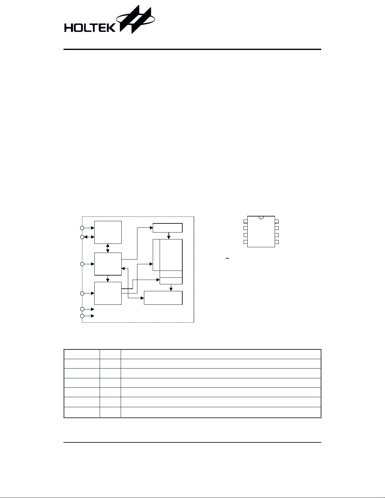
Block Diagram Pin Assignment
·
Partial page write allowed
·
8-byte Page write modes
·
Write operation with built-in timer
·
Hardware controlled write protection
·
40-year data retention
·
106erase/write cycles per word
·
Commerical temperature range (0°Cto+70°C)
·
8-pin DIP/SOP/TSSOP package
low power and low voltage operation are essential. Up
to eight HT24LC02 devices may be connected to the
same 2-wire bus. The HT24LC02 is guaranteed for 1M
erase/write cycles and 40-year data retention.
HT24LC02
S C L
S D A
W P
A 0 ~ A 2
V C C
V S S
I / O
C o n t r o l
L o g i c
M e m o r y
C o n t r o l
L o g i c
A d d r e s s
C o u n t e r
H V P u m p
X
D
E E P R O M
E
A r r a y
C
P a g e B u f
Y D E C
S e n s e A M P
R / W C o n t r o l
Pin Description
Pin Name I/O Description
A0~A2 I Address inputs
SDA I/O Serial data inputs/output
SCL I Serial clock data input
WP I Write protect
VSS
VCC
Negative power supply, ground
¾
Positive power supply
¾
V S S
A 0
1
A 1
2
A 2
3
4
V C C
8
W P
7
S C L
6
S D A
5
H T 2 4 L C 0 2
8 D I P - A / S O P - A / T S S O P - A
Rev. 1.10 1 November 5, 2002
Page 2
HT24LC02
Absolute Maximum Ratings
Operating Temperature (Commercial)..........................................................................................................0°Cto70°C
Storage Temperature.............................................................................................................................-50°Cto125°C
Applied VCC Voltage with Respect toVSS ................................................................................................-0.3V to 6.0V
Applied Voltage on any Pin withRespect to VSS ..............................................................................-0.3V to V
Note: These are stress ratings only. Stresses exceeding the range specified under ²Absolute Maximum Ratings² may
cause substantial damage to the device. Functional operation of this device at other conditions beyond those
listed in the specification is not implied and prolonged exposure to extreme conditions may affect device reliabil
ity.
CC
+0.3V
-
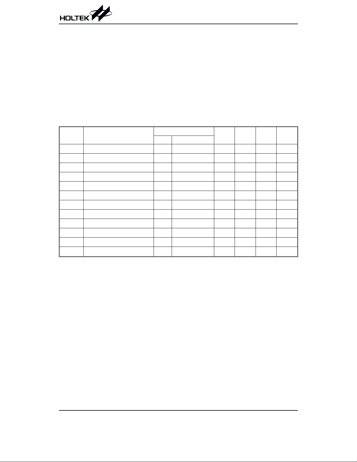
D.C. Characteristics
Symbol Parameter
V
I
CC1
I
CC2
V
V
V
I
LI
I
LO
I
STB1
I
STB2
C
C
CC
IL
IH
OL
IN
OUT
Operating Voltage
Operating Current 5V Read at 100kHz
Operating Current 5V Write at 100kHz
Input Low Voltage
Input High Voltage
Output Low Voltage 2.4V
Input Leakage Current 5V
Output Leakage Current 5V
Standby Current 5V
Standby Current 2.4V
Input Capacitance (See Note)
Output Capacitance (See Note)
Note: These parameters are periodically sampled but not 100% tested
Test Conditions
V
CC
Conditions
¾¾
¾¾ -1 ¾
¾¾
=2.1mA
I
OL
=0 or V
V
IN
V
OUT
V
IN
V
IN
=0 or V
=0 or V
=0 or V
CC
CC
CC
CC
¾ f=1MHz 25°C ¾¾
¾ f=1MHz 25°C ¾¾
Ta=0°Cto70°C
Min. Typ. Max. Unit
2.2
¾
¾¾
¾¾
0.7V
CC
¾
¾¾
¾¾
¾¾
¾¾
¾¾
5.5 V
2mA
5mA
0.3V
CC
V
+0.5
CC
0.4 V
1
1
5
4
6pF
8pF
V
V
mA
mA
mA
mA
Rev. 1.10 2 November 5, 2002
Page 3
HT24LC02
A.C. Characteristics
Symbol Parameter Remark
f
SK
t
HIGH
t
LOW
t
r
t
f
Clock Frequency
Clock High Time
Clock Low Time
SDA and SCL Rise Time Note
SDA and SCL Fall Time Note
¾¾
¾
¾
After this period the
t
HD:STA
START Condition Hold Time
first clock pulse is
generated
Only relevant for
t
SU:STA
START Condition Setup Time
repeated START
condition
t
HD:DAT
t
SU:DAT
t
SU:STO
t
AA
Data Input Hold Time
Data Input Setup Time
STOP Condition Setup Time
Output Valid from Clock
¾
¾
¾
¾¾
Time in which the bus
t
BUF
Bus Free Time
must be free before a
new transmission can
start
t
SP
t
WR
Input Filter Time Constant
(SDA and SCL Pins)
Write Cycle Time
Noise suppression
time
¾¾5¾
Note: These parameters are periodically sampled but not 100% tested
* The standard mode means V
=2.2V to 5.5V
CC
For relative timing, refer to timing diagrams
Standard Mode*
Ta=0°Cto70°C
V
=5V±10%
CC
Min. Max. Min. Max.
4000
4700
¾
¾
4000
4000
0
200
4000
4700
¾
100
¾
¾
1000
300
¾
¾
¾
¾
¾
3500
¾
100
¾
600
1200
¾
¾
600
600
100
600
¾
1200
¾
0
400 kHz
¾
¾
300 ns
300 ns
¾
¾
¾
¾
¾
900 ns
¾
50 ns
5ms
Unit
ns
ns
ns
ns
ns
ns
ns
ns
Rev. 1.10 3 November 5, 2002
Page 4
Functional Description
HT24LC02
·
Serial clock (SCL)
The SCL input is used for positive edge clock data into
each EEPROM device and negative edge clock data
out of each device.
·
Serial data (SDA)
The SDA pin is bidirectional for serial data transfer.
The pin is open-drain driven and may be wired-OR
with any number of other open-drain or open collector
devices.
·
A0, A1, A2
The A2, A1 and A0 pins are device address inputs that
are hard wired for the HT24LC02. As many as eight
2K devices may be addressed on a single bus system
(the device addressing is discussed in detail under the
Device Addressing section).
·
Write protect (WP)
The HT24LC02 has a write protect pin that provides
hardware data protection. The write protect pin allows
normal read/write operations when connected to the
V
. When the write protect pin is connected to Vcc,
SS
the write protection feature is enabled and operates
as shown in the following table.
WP Pin
Status
At V
CC
At V
SS
Full Array (2K)
Normal Read/Write Operations
Protect Array
Memory organization
·
HT24LC02, 2K Serial EEPROM
Internally organized with 256 8-bit words, the 2K requires an 8-bit data word address for random word ad
dressing.
Device operations
·
Clock and data transition
Data transfer may be initiated only when the bus is not
busy. During data transfer, the data line must remain
stable whenever the clock line is high. Changes in
data line while the clock line is high will be interpreted
as a START or STOP condition.
·
Start condition
A high-to-low transition of SDA with SCL high is a start
condition which must precede any other command
(refer to Start and Stop Definition Timing diagram).
·
Stop condition
A low-to-high transition of SDA with SCL high is a stop
condition. After a read sequence, the stop command
will place the EEPROM in a standby power mode (re
fer to Start and Stop Definition Timing Diagram).
·
Acknowledge
All addresses and data words are serially transmitted
to and from the EEPROM in 8-bit words. The
EEPROM sends a zero to acknowledge that it has re
ceived each word. This happens during the ninth clock
cycle.
D a t a a l l o w e d
t o c h a n g e
S D A
S C L
S t a r t
c o n d i t i o n
A d d r e s s o r
a c k n o w l e d g e
v a l i d
Device addressing
The 2K EEPROM devices all require an 8-bit device ad
dress word following a start condition to enable the chip
for a read or write operation. The device address word
consist of a mandatory one, zero sequence for the first
four most significant bits (refer to the diagram showing
the Device Address). This is common to all the
EEPROM device.
The next three bits are the A2, A1 and A0 device address bits for the 2K EEPROM. These three bits must
compare to their corresponding hard-wired input pins.
The 8th bit of device address is the read/write operation
select bit. A read operation is initiated if this bit is high
and a write operation is initiated if this bit is low.
If the comparison of the device address succeed the
EEPROM will output a zero at ACK bit. If not, the chip will
return to a standby state.
-
1 0
D e v i c e A d d r e s s
Write operations
·
Byte write
A write operation requires an 8-bit data word address
following the device address word and acknowledg
ment. Upon receipt of this address, the EEPROM will
again respond with a zero and then clock in the first
8-bit data word. After receiving the 8-bit data word, the
EEPROM will output a zero and the addressing de
vice, such as a microcontroller, must terminate the
write sequence with a stop condition. At this time the
EEPROM enters an internally-timed write cycle to the
non-volatile memory. All inputs are disabled during
-
this write cycle and EEPROM will not respond until the
write is completed (refer to Byte write timing).
S t o p
c o n d i t i o n
R / W1 0 A 2 A 1 A 0
-
-
-
-
Rev. 1.10 4 November 5, 2002
Page 5

·
Page write
The 2K EEPROM is capable of an 8-byte page write.
A page write is initiated the same as byte write, but the
microcontroller does not send a stop condition after
the first data word is clocked in. Instead, after the
EEPROM acknowledges the receipt of the first data
word, the microcontroller can transmit up to seven
more data words. The EEPROM will respond with a
zero after each data word received. The
microcontroller must terminate the page write se
quence with a stop condition.
The data word address lower three (2K) bits are inter
nally incremented following the receipt of each data
word. The higher data word address bits are not incre
mented, retaining the memory page row location (re
fer to Page write timing).
·
Acknowledge polling
Since the device will not acknowledge during a write
cycle, this can be used to determine when the cycle is
complete (this feature can be used to maximize bus
throughput). Once the stop condition for a write com
mand has been issued from the master, the device ini
tiates the internally timed write cycle. ACK polling can
be initiated immediately. This involves the master
sending a start condition followed by the control byte
for a write command (R/W=0). If the device is still busy
with the write cycle, then no ACK will be returned. If
the cycle is completed, then the device will return the
ACK and the master can then proceed with the next
read or write command.
·
Write protect
The HT24LC02 can be used as a serial ROM when
the WP pin is connected to VCC. Programming will be
inhibited and the entire memory will be
write-protected.
B y t e w r i t e t i m i n g
HT24LC02
S e n d W r i t e C o m m a n d
S e n d S t o p C o n d i t i o n
t o I n i t i a t e W r i t e C y c l e
S e n d S t a r t
S e n d C o t r o l l B y t e
-
-
-
-
·
Read operations
Read operations are initiated the same way as write
-
-
operations with the exception that the read/write se
lect bit in the device address word is set to one. There
are three read operations: current address read, ran
dom address read and sequential read.
·
Current address read
The internal data word address counter maintains the
last address accessed during the last read or write operation, incremented by one. This address stays valid
between operationsas long as the chip power is maintained. The address roll over during read from the last
byte of the last memory page to the first byte of the first
page. The address roll over during write from the last
byte of the current page to the first byte of the same
page. Once the device address with the read/write select bit set to one is clocked in and acknowledged by
the EEPROM, the current address data word is seri
w i t h R / W = 0
( A C K = 0 ) ?
N e x t O p e r a t i o n
N o
Y e s
Acknowledge polling flow
-
-
-
D e v i c e a d d r e s s W o r d a d d r e s s D A T A
S D A
S t a r t
A 1 A 0S P
A 2
R / W
A C K
A C K A C K
S t o p
P a g e w r i t e t i m i n g
D e v i c e a d d r e s s W o r d a d d r e s s D A T A n
S
S D A
S t a r t
A C K
A C K
D A T A n + 1 D A T A n + x
A C K
P
A C K
S t o p
C u r r e n t r e a d t i m i n g
D e v i c e a d d r e s s D A T A
S D A
S t a r t
A 1 A 0S P
A 2
A C K
Rev. 1.10 5 November 5, 2002
S t o p
N o A C K
Page 6

ally clocked out. The microcontroller does not respond
with an input zero but generates a following stop con
dition (refer to Current read timing).
·
Random read
A randomread requires a dummy byte write sequence
to load in the data word address which is then clocked
in and acknowledged by the EEPROM. The
microcontroller must then generate another start con
dition. The microcontroller now initiates a current ad
dress read by sending a device address with the
read/write select bit high. The EEPROM acknowl
edges the device address and serially clocks out the
data word. The microcontroller does not respond with
a zero but does generates a following stop condition
(refer to Random read timing).
R a n d o m r e a d t i m i n g
HT24LC02
·
Sequential read
-
-
-
-
Sequential reads are initiated by either a current ad
dress read or a random address read. After the
microcontroller receives a data word, it responds with an
acknowledgment. As long as the EEPROM receives an
acknowledgment, it will continue to increment the data
word address and serially clock out sequential data
words. When the memory address limit is reached, the
data word address will roll over and the sequential read
continues. The sequential read operation is terminated
when the microcontroller does not respond with a zero
but generates a following stop condition.
-
D e v i c e a d d r e s s W o r d a d d r e s s
S D A
S
S t a r t
A 2 A 1 A 0
S e q u e n t i a l r e a d t i m i n g
D e v i c e a d d r e s s D A T A n
S
S D A
S t a r t
Timing Diagrams
S C L
t
S U:S T A
t
S D A
S D A
O U T
S P
A C K
D A T A
t
S U:S T O
t
B U F
S t o p
P
N o A C K
P
A C K
S t o p
D e v i c e a d d r e s s
S
A C K
A C K
t
f
t
L O W
t
H D:S T A
t
A A
t
t
r
A C K
S t a r t
D A T A n + 1 D A T A n + x
A C K
H I G H
t
t
H D:D A T
V a l i d V a l i d
S U:D A T
S C L
S D A
Note:
8 t h b i t
W o r d n
A C K
The write cycle time t
t
W R
S t o p
C o n d i t i o n
is the time from a valid stop condition of a write sequence to the end of the valid start
WR
S t a r t
C o n d i t i o n
condition of sequential command.
Rev. 1.10 6 November 5, 2002
Page 7

Package Information
8-pin DIP (300mil) outline dimensions
B
C
D
HT24LC02
A
8
5
4
1
H
G
E
F
=
I
Symbol
Min. Nom. Max.
A 355
B 240
C 125
D 125
E16
F50
G
¾
H 295
I 335
Dimensions in mil
¾
¾
¾
¾
¾
¾
100
¾
¾
a 0°¾15°
375
260
135
145
20
70
¾
315
375
Rev. 1.10 7 November 5, 2002
Page 8

8-pin SOP (150mil) outline dimensions
5
8
A
1
B
4
C
HT24LC02
C '
D
E
F
Symbol
Min. Nom. Max.
A 228
B 149
C14
C¢
189
D53
E
¾
F4
G22
H4
G
H
=
Dimensions in mil
¾
¾
¾
¾
¾
50
¾
¾
¾
a 0°¾10°
244
157
20
197
69
¾
10
28
12
Rev. 1.10 8 November 5, 2002
Page 9

8-pin TSSOP outline dimensions
HT24LC02
58
E 1
1 4
E
L 1
Dimensions in mm
¾
¾
¾
0.25
¾
¾
¾
¾
0.65
¾
¾
G
A
e
R 0 . 1 0
( 4 C O R N E R S )
Symbol
A 1.05
A1 0.05
A2 0.95
B
C 0.11
D 2.90
E 6.20
E1 4.30
e
L 0.50
L1 0.90
y
D
A 2
A 1
B
y
L
C
Min. Nom. Max.
¾
¾
¾¾
q 0°¾8°
1.20
0.15
1.05
¾
0.15
3.10
6.60
4.50
¾
0.70
1.10
0.10
Rev. 1.10 9 November 5, 2002
Page 10

Product Tape and Reel Specifications
Reel dimensions
HT24LC02
T 2
A
B
T 1
D
SOP 8N
Symbol Description Dimensions in mm
A Reel Outer Diameter
B Reel Inner Diameter
C Spindle Hole Diameter
D Key Slit Width
T1 Space Between Flange
T2 Reel Thickness
330±1.0
62±1.5
13.0+0.5
2.0±0.15
12.8+0.3
18.2±0.2
C
-0.2
-0.2
TSSOP 8L
Symbol Description Dimensions in mm
A Reel Outer Diameter
B Reel Inner Diameter
C Spindle Hole Diameter
D Key Slit Width
T1 Space Between Flange
T2 Reel Thickness
330±1.0
62±1.5
13.0+0.5
-0.2
2.0±0.5
12.8+0.3
-0.2
18.2±0.2
Rev. 1.10 10 November 5, 2002
Page 11

Carrier tape dimensions
HT24LC02
D
E
F
PD 1
P 1P 0
W
A 0
B 0
C
SOP 8N
Symbol Description Dimensions in mm
W Carrier Tape Width
P Cavity Pitch
E Perforation Position
F Cavity to Perforation (Width Direction)
D Perforation Diameter
12.0+0.3
8.0±0.1
1.75±0.1
5.5±0.1
1.55±0.1
D1 Cavity Hole Diameter 1.5+0.25
P0 Perforation Pitch
P1 Cavity to Perforation (Length Direction)
A0 Cavity Length
B0 Cavity Width
K0 Cavity Depth
t Carrier Tape Thickness
4.0±0.1
2.0±0.1
6.4±0.1
5.20±0.1
2.1±0.1
0.3±0.05
C Cover Tape Width 9.3
t
K 0
-0.1
TSSOP 8L
Symbol Description Dimensions in mm
W Carrier Tape Width
P Cavity Pitch
E Perforation Position
F Cavity to Perforation (Width Direction)
12.0+0.3
-0.1
8.0±0.1
1.75±0.1
5.5±0.5
D Perforation Diameter 1.5+0.1
D1 Cavity Hole Diameter 1.5+0.1
P0 Perforation Pitch
P1 Cavity to Perforation (Length Direction)
A0 Cavity Length
B0 Cavity Width
K0 Cavity Depth
t Carrier Tape Thickness
4.0±0.1
2.0±0.1
7.0±0.1
3.6±0.1
1.6±0.1
0.3±0.013
C Cover Tape Width 9.3
Rev. 1.10 11 November 5, 2002
Page 12

HT24LC02
Holtek Semiconductor Inc. (Headquarters)
No.3, Creation Rd. II, Science-based Industrial Park, Hsinchu, Taiwan
Tel: 886-3-563-1999
Fax: 886-3-563-1189
http://www.holtek.com.tw
Holtek Semiconductor Inc. (Sales Office)
11F, No.576, Sec.7 Chung Hsiao E. Rd., Taipei, Taiwan
Tel: 886-2-2782-9635
Fax: 886-2-2782-9636
Fax: 886-2-2782-7128 (International sales hotline)
Holtek Semiconductor (Shanghai) Inc.
7th Floor, Building 2, No.889, Yi Shan Rd., Shanghai, China
Tel: 021-6485-5560
Fax: 021-6485-0313
http://www.holtek.com.cn
Holtek Semiconductor (Hong Kong) Ltd.
RM.711, Tower 2, Cheung Sha Wan Plaza, 833 Cheung Sha Wan Rd., Kowloon, Hong Kong
Tel: 852-2-745-8288
Fax: 852-2-742-8657
Holmate Semiconductor, Inc.
48531 Warm Springs Boulevard, Suite 413, Fremont, CA 94539
Tel: 510-252-9880
Fax: 510-252-9885
http://www.holmate.com
Copyright Ó 2002 by HOLTEK SEMICONDUCTOR INC.
The information appearing in this Data Sheet is believed to be accurate at the time of publication. However, Holtek as
sumes no responsibility arising from the use of the specifications described. The applications mentioned herein are used
solely for the purpose of illustration and Holtek makes no warranty or representation that such applications will be suitable
without further modification, nor recommends the use of its products for application that may present a risk to human life
due to malfunction or otherwise. Holtek reserves the right to alter its products without prior notification. For the most
up-to-date information, please visit our web site at http://www.holtek.com.tw.
-
Rev. 1.10 12 November 5, 2002
 Loading...