

Page 1
DS92LV222A
Two Channel Bus LVDS MUXed Repeater
DS92LV222A Two Channel Bus LVDS MUXed Repeater
May 1998
General Description
The DS92LV222Ais a repeater designed specifically for the
bridging of multiple backplanes in a rack. The DS92LV222A
utilizes low voltagedifferential signaling to deliver high speed
while consuming minimal power with reduced EMI. The
RSEL pin and DE pins allow maximum flexibility as to which
receiver/driver are used. The DS92LV222A repeats signals
between backplanes and accepts or drives signals onto the
local bus. It also features a flow through pin out which allows
easy PCB routing for short stubs between its pins and the
connector.
The driver is selectable between 3.5 mA(100Ω load) and 8.5
mA (27Ω load) output loop currents depending upon the
level applied to the ISEL pin. This allows for single termination (point-to-point) and also double termination (multipoint)
applications while maintain similar differential levels.
The receiver threshold is
common mode range.
±
100 mV, while providing±1V
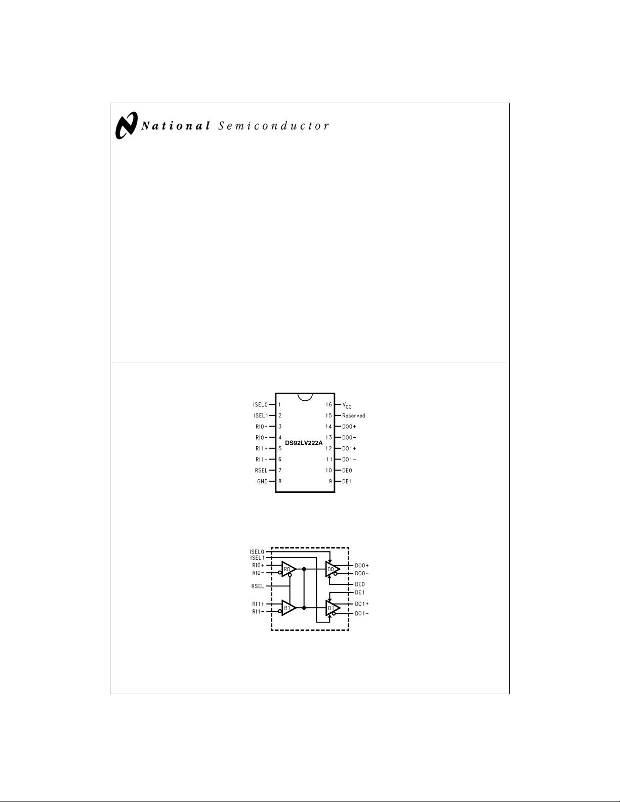
Connection Diagram
Features
n Bus LVDS Signaling (BLVDS)
n Designed for Double Termination Applications
n Low power CMOS design
n High Signaling Rate Capability (above 100 Mbps)
n Ultra Low Power Dissipation (13.2 mW quiescent)
n Balanced Output Impedance
n Lite Bus Loading 5 pF typical
n Selectable Drive Capability (3.5 mA or 8.5 mA)
n 3.3V operation
±
n
1V Common Mode Range
±
n
100 mV Receiver Sensitivity
n Available in 16 pin SOIC package.
DS100055-1
Order Number DS92LV222ATM
See NS Package Number M16A
Block Diagram
DS100055-2
TRI-STATE®is a registered trademark of National Semiconductor Corporation.
© 1998 National Semiconductor Corporation DS100055 www.national.com
Page 2
Absolute Maximum Ratings (Notes 1, 2)
If Military/Aerospace specified devices are required,
please contact the National Semiconductor Sales Office/
Distributors for availability and specifications.
Supply Voltage (V
Enable Input Voltage (DE) −0.3V to (V
Current Select Voltage
(ISEL) −0.3V to (V
Receiver Select Voltage
(RSEL) −0.3V to (V
Bus Pin Voltage (DO/RI
Driver Short Circuit Current Continuous
ESD (HBM 1.5 kΩ, 100 pF)
) 6.0V
CC
CC
CC
±
) −0.3V to +3.9V
CC
+ 0.3V)
+ 0.3V)
+ 0.3V)
>
2kV
Derate SOIC Package
above 25˚C 8mW/˚C
Storage Temperature Range −65˚C to +150˚C
Lead Temperature
(Soldering, 4 sec.) 260˚C
Recommended Operating
Conditions
Min Max Units
Supply Voltage (V
Receiver Input Voltage 0.0 2.9 V
Operating Free Air Temperature −40 +85 ˚C
) 3.0 3.6 V
CC
Maximum Package Power Dissipation at 25˚C
SOIC 970 mW
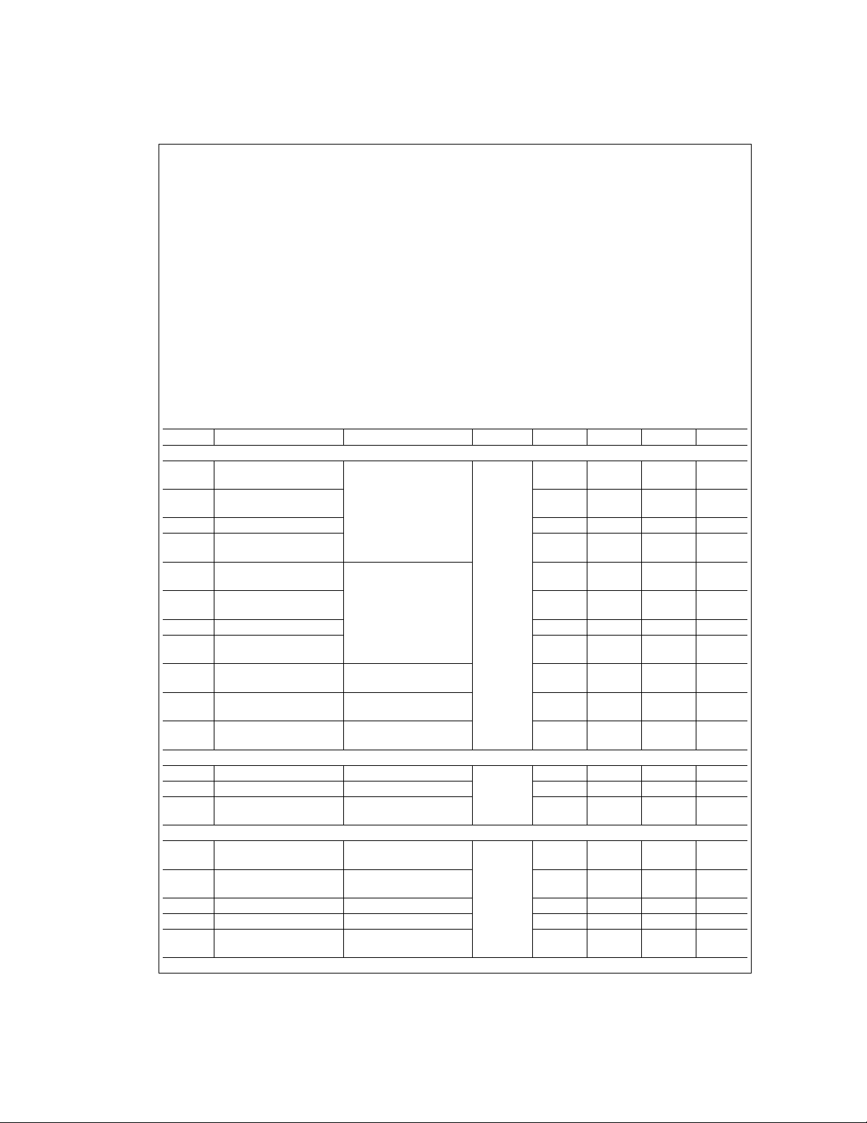
DC Electrical Characteristics
TA= −40˚C to +85˚C unless otherwise noted, VCC= 3.3V±0.3V (Notes 2, 3)
Symbol Parameter Conditions Pin Min Typ Max Units
DIFFERENTIAL DRIVER CHARACTERISTICS
V
OD
∆V
V
OS
∆V
V
OD
∆V
V
OS
∆V
I
OZD
I
OXD
I
OSD
OD
Output Differential
Voltage
VOD Magnitude
Change
RL=27Ω
Isel = 0V
Offset Voltage 1.0 1.25 1.6 V
Offset Magnitude
OS
Change
OD
Output Differential
Voltage
VOD Magnitude
Change
RL= 100Ω
Isel = 3.3V
Offset Voltage 0.9 1.25 1.6 V
Offset Magnitude
OS
Change
TRI-STATE®Leakage VO=VCCor GND,
DE=0
Power-Off Leakage VO= 2.9V or GND,
=0V
V
Output Short Circuit
Current
CC
ISEL = V
VO=0V
DIFFERENTIAL RECEIVER CHARACTERISTICS
V
TH
V
TL
I
IN
Input Threshold High RI+, RI− +100 mV
Input Threshold Low −100 mV
Input Current VIN= +2.9V, or 0V, V
=3.6Vor0V
DEVICE CHARACTERISTICS
V
IH
V
IL
I
IH
I
IL
V
CL
Minimum Input High
Voltage
Maximum Input Low
Voltage
Input High Current VIN=VCCor 2.4V
Input Low Current VIN= GND or 0.4V
Input Diode Clamp
Voltage
I
CLAMP
Figure 1
DO+,
DO−
Figure 1
CC
CC
DE0,
DE1,
RSEL,
ISEL0,
ISEL1
= −18 mA −1.5 −0.8 V
170 220 280 mV
210mV
10 20 mV
250 360 480 mV
210mV
10 20 mV
±
1
±
1
±
10 µA
±
10 µA
−11 −13 mA
−10
2.0 V
±
1 +10 µA
CC
GND 0.8 V
±
1
±
1
±
10 µA
±
10 µA
V
www.national.com 2
Page 3
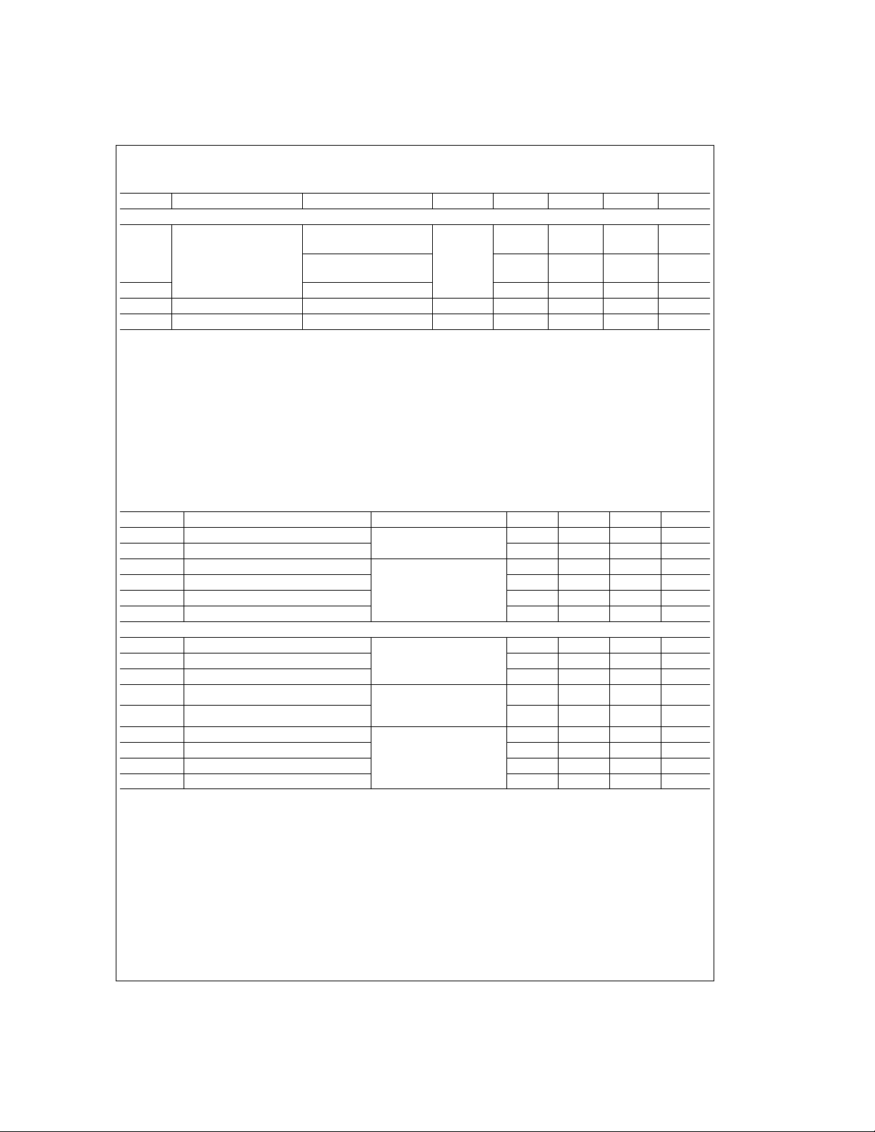
DC Electrical Characteristics (Continued)
TA= −40˚C to +85˚C unless otherwise noted, VCC= 3.3V±0.3V (Notes 2, 3)
Symbol Parameter Conditions Pin Min Typ Max Units
DEVICE CHARACTERISTICS
I
CCD
I
CCZ
C
input
C
output
Note 1: “Absolute Maximum Ratings” are these beyond which the safety of the device cannot be guaranteed. They are not meant to imply that the device should
be operated at these limits. The table of “Electrical Characteristics” provides conditions for actual device operation.
Note 2: All currents into device pins are positive; all currents out of device pins are negative.All voltages are referenced to device ground unless otherwise specified.
Note 3: All typicals are given for V
Note 4: ESD Rating: HBM (1.5 kΩ, 100 pF)
Note 5: CL includes probe and fixture capacitance.
Note 6: Generator waveforms for all tests unless otherwise specified: f = 1MHz, ZO = 50Ω,t
Note 7: The DS92LV222A is a current mode device and only functions datasheet specifications when a resistive load is applied to the drivers outputs.
Note 8: During receiver select transition(s), data must be held in a steady state 15 ns before and 15 ns after the RSEL pin changes state.
Note 9: Channel-to-channel skew is the measurement between outputs of D0 and D1.
Power Supply Current No Load; DE = RSEL =
Isel=0V
V
CC
=27Ω; DE = RSEL
R
L
Isel=0V
=V
CC
DE = 0V; RSEL = V
Capacitance at RO+/RO- 5 pF
Capacitance at DO+/DO- 5 pF
= +3.3V and TA= +25˚C, unless otherwise stated.
CC
>
2 kV EIAJ (0Ω, 200 pF)>200V
V
CC
25 45 mA
24 40 mA
CC
=<6.0 ns (0%–100%).
f
48mA
AC Electrical Characteristics
TA= −40˚C to +85˚C, VCC= 3.3V±0.3V (Note 6)
Symbol Parameter Conditions Min Typ Max Units
t
TLH
t
THL
t
PHZ
t
PLZ
t
PZH
t
PZL
Transition Time Low to High RL=27Ω
Transition Time High to Low 0.15 0.4 2.0 ns
CL=10pF
Disable Time High to Z RL=27Ω
Disable Time Low to Z 2.0 6.0 9.0 ns
CL=10pF
Enable Time Z to High 2.0 6.0 9.0 ns
Enable Time Z to Low 2.0 6.0 9.0 ns
DIFFERENTIAL RECEIVER TO DRIVER TIMING REQUIREMENTS
t
PHL_RD
t
PLH_RD
t
SK_RD
t
PHL_RS0
t
PLH_RS1
t
PHL_R0D
t
PLH_R0D
t
PHL_R1D
t
PLH_R1D
Differential Prop. Delay High to Low RL=27Ω
Differential Prop. Delay Low to High 3.0 8.0 13 ns
Pulse SKEW |t
| 0 0.3 2.0 ns
PHL–tPLH
CL=10pF
Prop. Delay High to Low RSEL to Driver Outputs
Prop. Delay Low to High 2.0 8.0 13 ns
Channel-to-Channel Skew R0to D
x
Channel-to-Channel Skew R0to D
x
Channel-to-Channel Skew R1to D
x
Channel-to-Channel Skew R1to D
x
R
CL= 10 pF (Note 8)
RL=27Ω
x
C
x
(Note 9)
x
x
=27Ω
L
=10pF
L
Figures 2, 3
Figures 2, 3
Figures 4, 5
Figures 4, 5
Figures 2, 3
Figures 2, 3
Figures 6, 7
0.15 0.4 2.0 ns
2.0 6.0 9.0 ns
3.0 7.7 13 ns
2.0 7.5 13 ns
0.3 0.8 ns
0.3 0.8 ns
0.3 0.8 ns
0.3 0.8 ns
3 www.national.com
Page 4

Test Circuits and Timing Waveforms
FIGURE 1. Differential Driver DC Test Circuit
FIGURE 2. Differential Receiver to Driver Propagation Delay and Driver Transition Time Test Circuit
DS100055-3
DS100055-4
FIGURE 3. Differential Receiver to Driver Propagation Delay and Driver Transition Time Waveforms
FIGURE 4. Driver TRI-STATE Delay Test Circuit
www.national.com 4
DS100055-5
DS100055-6
Page 5

Test Circuits and Timing Waveforms (Continued)
FIGURE 5. Driver TRI-STATE Delay Waveforms
FIGURE 6. Receiver Select to Driver Propagation Delay Test Circuit
DS100055-7
DS100055-8
Pin Description
Pin Name Number
±
RI
±
DO
RSEL 1 I Receiver Select TTL Input, (see Truth Tables)
DE 2 I Driver Enable TTL Input, Active High
ISEL 2 I IOL Control Pin (Select High = 3.5 mA (100Ω Load),
GND 1 NA Ground Reference
V
CC
Reserved 1 NA Reserved Pin
FIGURE 7. Receiver Select to Driver Propagation Delay Waveforms
of Pins
Input/
Output
Description
4 I Bus LVDS Receiver Inputs
4 O Bus LVDS Driver Outputs
Select Low = 8.5mA (27Ω Load))
1 NA Power Supply
5 www.national.com
DS100055-9
Page 6

Function Select Table
Receiver Zero ON, Driver Zero ON, Driver One OFF H L L
Receiver Zero ON, Driver Zero OFF, Driver One ON L H L
Receiver One ON, Driver Zero ON, Driver One OFF H L H
Receiver One ON, Driver Zero OFF, Driver One ON L H H
Receiver Zero ON, Driver Zero ON, Driver One ON H H L
Receiver One ON, Driver Zero ON, Driver One ON H H H
Driver Zero and Driver One TRI-STATE L L X
MODE SELECTED DE0 DE1 RSEL
Truth Table for Receiver Zero
INPUTS OUTPUTS
DE0 RSEL (RI0+)–(RI0−) DO+ DO−
HL L LH
HL H HL
H L 100 mV
LX X ZZ
X = High or low logic state
Z = High impedance state
L = Low state
>&>
−100 mV X X
Truth Table for Current Drive
Driver Current Drive ISEL0 ISEL1
Driver 0 3.5 mA H X
Driver 0 8.5 mA L X
Driver 1 3.5 mA X H
Driver 1 8.5 mA X L
Applications Information
There are few common practices which should be employed
when designing PCB for Bus LVDS signaling. Recommended practices are:
Use at least 4 PCB board layer (Bus LVDS signals,
•
ground, power and TTL signals).
Keep drivers and receivers as close to the (Bus LVDS
•
port side) connector as possible.
Bypass each Bus LVDS device and also use distributed
•
bulk capacitance. Surface mount capacitors placed close
to power and ground pins work best. Two or three multilayer ceramic (MLC) surface mount capacitors (0.1µ and
0.01 µF in parallel should be used between each V
ground. The capacitors should be as close as possible to
the V
pin.
CC
Use controlled impedance traces which match the differ-
•
ential impedance of your transmission medium (i.e.,
Cable) and termination resistor.
Use the termination resistor which best matches the dif-
•
ferential impedance of your transmission line.
Leave unused Bus LVDS receiver inputs open (floating).
•
Isolate TTL signals from Bus LVDS signals.
•
MEDIA (CABLE, CONNECTOR OR BACKPLANE)
SELECTION:
Use controlled impedance media. The cables and con-
•
nectors should have a matched differential impedance.
and
CC
Truth Table for Receiver One
INPUTS OUTPUTS
DE1 RSEL (RI1+)–(RI1−) DO+ DO−
HH L LH
HH H HL
H H 100 mV
LX X ZZ
X = High or low logic state
Z = High impedance state
L = Low state
Balanced cables (e.g., twisted pair) are usually better
•
than unbalanced cables (ribbon cable, simple coax) for
noise reduction and signal quality.
•
There are different types of failsafe situations to consider,
•
these are Open Input, Terminated Input, and other special cases. The first, Openinput failsafe occurs when only
one receiver is being used (R0 for example). The unused
receiver (R1) inputs should be left open for noise minimization. The second case is for terminated inputs. This occurs when theinputs have a low impedance (typically 100
Ohm) termination (R
plugged. For this case, and if the output state needs to
maintain a known state, two external bias resistors may
be used to provide a strong common mode bias point.
For this a 10K Ohm pull up and pull down resistor may be
used to set the output high. Note that R
be much larger ( 2 orders of magnitude) compared to R
to minimize loading effects to the Bus LVDS driver when
it is active.
>&>
−100 mV X X
) across them, and the cable is un-
T
and R2should
1
T
www.national.com 6
Page 7

Applications Information (Continued)
FIGURE 8. Terminated Input Failsafe Circuit
DS100055-10
7 www.national.com
Page 8

Physical Dimensions inches (millimeters) unless otherwise noted
Order Number DS92LV222ATM
NS Package Number M16A
DS92LV222A Two Channel Bus LVDS MUXed Repeater
LIFE SUPPORT POLICY
NATIONAL’S PRODUCTS ARE NOT AUTHORIZED FOR USE AS CRITICAL COMPONENTS IN LIFE SUPPORT DEVICES OR SYSTEMS WITHOUT THE EXPRESS WRITTEN APPROVAL OF THE PRESIDENT OF NATIONAL SEMICONDUCTOR CORPORATION. As used herein:
1. Life support devices or systems are devices or systems which, (a) are intended for surgical implant into
the body, or (b) support orsustain life, and whose failure to perform when properly used in accordance
with instructions for use provided in the labeling, can
be reasonably expected toresult in a significant injury
to the user.
National Semiconductor
Corporation
Americas
Tel: 1-800-272-9959
Fax: 1-800-737-7018
Email: support@nsc.com
www.national.com
National does not assume any responsibility for use of any circuitry described, no circuit patent licenses are implied and National reserves the right at any time without notice to change said circuitry and specifications.
National Semiconductor
Europe
Fax: +49 (0) 1 80-530 85 86
Email: europe.support@nsc.com
Deutsch Tel: +49 (0) 1 80-530 85 85
English Tel: +49 (0) 1 80-532 78 32
Français Tel: +49 (0) 1 80-532 93 58
Italiano Tel: +49 (0) 1 80-534 16 80
2. A critical component in any component of a life support
device or system whose failure to perform can be reasonably expected to cause the failure of the life support
device or system, orto affect its safety or effectiveness.
National Semiconductor
Asia Pacific Customer
Response Group
Tel: 65-2544466
Fax: 65-2504466
Email: sea.support@nsc.com
National Semiconductor
Japan Ltd.
Tel: 81-3-5620-6175
Fax: 81-3-5620-6179
 Loading...