

Page 1
DS92LV040A
4 Channel Bus LVDS Transceiver
DS92LV040A 4 Channel Bus LVDS Transceiver
August 2002
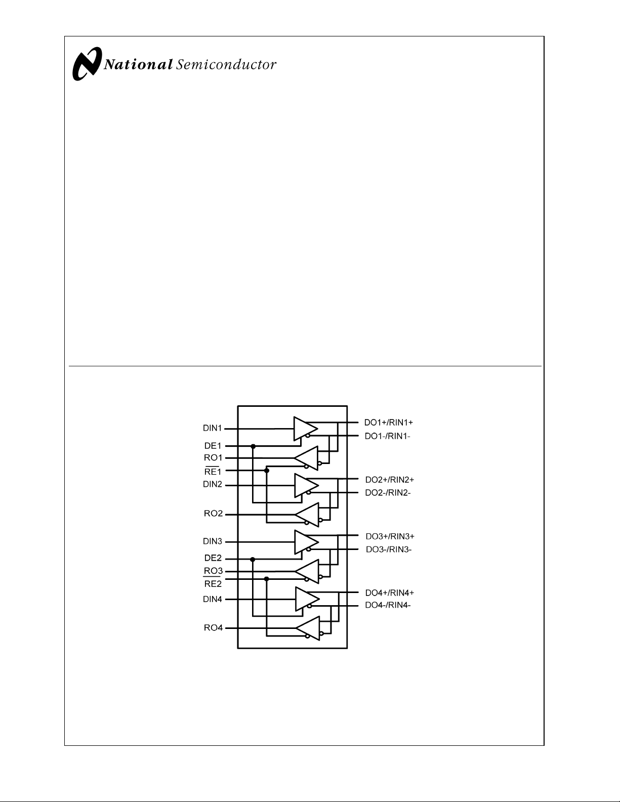
General Description
The DS92LV040A is one in a series of Bus LVDS transceivers designed specifically for high speed, low power backplane or cable interfaces. The device operates from a single
3.3V power supply and includes four differential line drivers
and four receivers. To minimize bus loading, the driver outputs and receiver inputs are internally connected. The device
also features a flow through pin out which allows easy PCB
routing for short stubs between its pins and the connector.
The driver translates 3V LVTTL levels (single-ended) to differential Bus LVDS (BLVDS) output levels. This allows for
high speed operation while consuming minimal power and
reducing EMI. In addition, the differential signaling provides
common mode noise rejection greater than
The receiver threshold is less than +0/−70 mV. The receiver
translates the differential Bus LVDS to standard (LVTTL/
LVCMOS) levels. (See Applications Information Section for
more details.)
±
1V.
Simplified Functional Diagram
Features
n Bus LVDS Signaling
n Propagation delay: Driver 2.3ns max, Receiver 3.2ns
max
n Low power CMOS design
n 100% Transition time 1ns driver typical, 1.3ns receiver
typical
n High Signaling Rate Capability (above 155 Mbps)
n 0.1V to 2.3V Common Mode Range for V
n 70 mV Receiver Sensitivity
n Supports open and terminated failsafe on port pins
n 3.3V operation
n Glitch free power up/down (Driver & Receiver disabled)
n Light Bus Loading (5 pF typical) per Bus LVDS load
n Designed for Double Termination Applications
n Balanced Output Impedance
n Product offered in 44 pin LLP (Leadless Leadframe
Package) package
n High impedance Bus pins on power off (V
= 200mV
ID
= 0V)
CC
10133601
© 2002 National Semiconductor Corporation DS101336 www.national.com
Page 2
Absolute Maximum Ratings (Notes 1,
2)
If Military/Aerospace specified devices are required,
please contact the National Semiconductor Sales Office/
DS92LV040A
Distributors for availability and specifications.
Supply Voltage (V
Enable Input Voltage
(DE, RE)
Driver Input Voltage (D
Receiver Output Voltage
(R
) −0.3V to (VCC+0.3V)
OUT
Bus Pin Voltage (DO/RI
ESD (Note 4)
(HBM 1.5 kΩ, 100 pF)
Machine Model
Maximum Package Power Dissipation at 25˚C
LLP(Note 3) 4.8 W
) 4.0V
CC
−0.3V to (VCC+0.3V)
) −0.3V to (VCC+0.3V)
IN
±
) −0.3V to +3.9V
>
>
4kV
250V
θ
(Note 3) 25.8˚C/W
ja
θ
jc
25.5˚C/W
Storage Temperature Range −65˚C to +150˚C
Lead Temperature
(Soldering, 4 sec.) 260˚C
Recommended Operating Conditions
Min Max Units
Supply Voltage (V
Receiver Input Voltage 0.0 2.4 V
Operating Free Air Temperature −40 +85 ˚C
Slowest Input Edge Rate
(Note 7)(20% to 80%) ∆t/∆V
Data 1.0 ns/V
Control 3.0 ns/V
) 3.0 3.6 V
CC
Derate LLP Package 38.8mW/˚C
DC Electrical Characteristics
Over recommended operating supply voltage and temperature ranges unless otherwise specified (Notes 2, 4)
Symbol Parameter Conditions Pin Min Typ Max Units
V
∆V
V
∆V
V
V
I
OSD
V
V
I
OD
V
V
V
I
IN
OD
OS
OHD
OLD
OHR
OLR
TH
TL
CMR
Output Differential
Voltage
VODMagnitude Change 527mV
OD
RL=27Ω, Figure 1 DO+/RI+,
DO−/RI−
200 300 460 mV
Offset Voltage 1.1 1.3 1.5 V
Offset Magnitude Change 5 10 mV
OS
Driver Output High
Voltage
Driver Output Low
Voltage
Driver Output Short
Circuit Current (Note 11)
Receiver Voltage Output
High (Note 12)
Receiver Voltage Output
Low
Receiver Output Dynamic
Current (Note 11)
Input Threshold High
(Note 9)
Input Threshold Low
(Note 9)
Receiver Common Mode
Range
Input Current DE = 0V, RE = 2.4V,
RL=27Ω
RL=27Ω
VOD= 0V, DE = VCC, Driver outputs
shorted together
VID= +300 mV IOH=−4mA R
OUT
Inputs Open V
Inputs Terminated,
RL=27Ω
IOL= 4.0 mA, VID= −300 mV
VID= 300mV, V
V
= −300mV, V
ID
OUT=VCC
OUT
−1.0V −50 |33| mA
= 1.0V |36| 60 mA
DE = 0V, Over common mode range DO+/RI+,
DO−/RI−
VIN= +2.4V or 0V
V
= 0V, VIN= +2.4V or 0V −20
CC
1.4 1.65 V
0.95 1.1 V
|30| | 45| mA
VCC−0.2 V
−0.2 V
CC
V
−0.2 V
CC
0.05 0.100 V
−40 0 mV
−70 −40 mV
|VID|/2 2.4 −
|/2
|V
ID
−20
±
1 +20 µA
±
1 +20 µA
V
www.national.com 2
Page 3
DC Electrical Characteristics (Continued)
Over recommended operating supply voltage and temperature ranges unless otherwise specified (Notes 2, 4)
Symbol Parameter Conditions Pin Min Typ Max Units
V
IH
V
IL
I
IH
I
IL
V
CL
I
CCD
I
CCR
I
CCZ
I
CC
I
OFF
C
OUTPUT
c
OUTPUT
Minimum Input High
Voltage
Maximum Input Low
Voltage
DIN, DE,
RE
2.0 V
GND 0.8 V
Input High Current VIN=VCCor 2.4V −20
Input Low Current VIN= GND or 0.4V −20
Input Diode Clamp
Voltage
Power Supply Current
Drivers Enabled,
I
= −18 mA
CLAMP
No Load, DE = RE = V
DIN=VCCor GND
−1.5 −0.8 V
,
CC
V
CC
Receivers Disabled
Power Supply Current
DE=RE=0V,V
=±300mV
ID
Drivers Disabled,
Receivers Enabled
Power Supply Current,
Drivers and Receivers
DE = 0V; RE = V
DIN=VCCor GND 28 40 mA
,
CC
TRI-STATE
Power Supply Current,
Drivers and Receivers
Enabled
Power Off Leakage
Current
DE=V
DIN=VCCor GND,
R
L
VCC= 0V or OPEN,
D
IN
V
APPLIED
;RE=0V,
CC
=27Ω
, DE, RE = 0V or OPEN,
= 3.6V (Port Pins)
DO+/RI+,
DO−/RI− −20 +20 µA
Capacitance@Bus Pins DO+/RI+,
DO−/RI−
Capacitance@R
OUT
R
OUT
CC
±
2.5 +20 µA
±
2.5 +20 µA
V
20 40 mA
27 40 mA
70 100 mA
5pF
5pF
DS92LV040A
AC Electrical Characteristics
Over recommended operating supply voltage and temperature ranges unless otherwise specified (Note 7)
Symbol Parameter Conditions Min Typ Max Units
DIFFERENTIAL DRIVER TIMING REQUIREMENTS
t
PHLD
t
PLHD
t
SKD1
t
CCSK
t
TLH
t
THL
t
PHZ
t
PLZ
t
PZH
t
PZL
f
MAXD
Differential Prop. Delay High to Low (Note 9) RL=27Ω,
Differential Prop. Delay Low to High (Note 9) 1.0 1.5 2.3 ns
Differential Skew |t
PHLD–tPLHD
| (duty cycle)(Note 10),
Figures 2, 3,
=10pF
C
L
(Note 9)
1.0 1.5 2.3 ns
80 160 ps
Channel to Channel Skew (all 4 channels), (Note 9) 220 400 ps
Transition Time Low to High (20% to 80%) 0.4 0.75 1.3 ns
Transition Time High to Low (80% to 20%) 0.4 0.75 1.3 ns
Disable Time High to Z RL=27Ω,
Disable Time Low to Z 5.0 10 ns
Enable Time Z to High 5.0 10 ns
Figures 4, 5,
=10pF
C
L
5.0 10 ns
Enable Time Z to Low 5.0 10 ns
Guaranteed operation per data sheet up to the Min.
Duty Cycle 45/55%,Transition time ≤ 25% of period
85 125 MHz
(Note 9)
www.national.com3
Page 4
AC Electrical Characteristics (Continued)
Over recommended operating supply voltage and temperature ranges unless otherwise specified (Note 7)
Symbol Parameter Conditions Min Typ Max Units
DIFFERENTIAL RECEIVER TIMING REQUIREMENTS
DS92LV040A
t
PHLDR
t
PLHDR
t
SDK1R
Differential Prop. Delay High to Low (Note 9) Figures 6, 7,
=15pF
Differential Prop Delay Low to High (Note 9) 1.6 2.4 3.2 ns
Differential Skew |t
PHLD–tPLHD
| (duty cycle)(Note 10),
C
L
(Note 9)
t
CCSKR
t
TLHR
t
THLR
t
PHZ
t
PLZ
t
PZH
t
PZL
f
MAXR
Channel to Channel Skew (all 4 channels)(Note 9) 140 300 ps
Transition Time Low to High (10% to 90%) (Note 9) 0.850 1.250 2.0 ns
Transition Time High to Low (90% to 10%) (Note 9) 0.850 1.030 2.0 ns
Disable Time High to Z RL= 500Ω,
Disable Time Low to Z 3.0 10 ns
Enable Time Z to High 3.0 10 ns
Figures 8, 9,
=15pF
C
L
Enable Time Z to Low 3.0 10 ns
Guaranteed operation per data sheet up to the Min.
Duty Cycle 45/55%,Transition time ≤ 25% of period
(Note 9)
Note 1: “Absolute Maximum Ratings” are those values beyond which the safety of the device cannot be guaranteed. They are not meant to imply that the devices
should be operated at these limits. The table of “Electrical Characteristics” provides conditions for actual device operation.
Note 2: All currents into device pins are positive; all currents out of device pins are negative.All voltages are referenced to ground unless otherwise specified except
V
, ∆VODand VID.
OD
Note 3: Package must be mounted to pc board in accordance with AN-1187 to achieve thermals.
Note 4: All typicals are given for V
Note 5: ESD Rating: HBM (1.5 kΩ, 100 pF)
Note 6: C
Note 7: Generator waveforms for all tests unless otherwise specified:f=25MHz, Z
minimum skew, data input edge rates should be equal to or faster than 1ns/V; control signals equal to or faster than 3ns/V. In general, the faster the input edge rate,
the better the AC performance.
Note 8: The DS92LV040A functions within datasheet specification when a resistive load is applied to the driver outputs.
Note 9: Propagation delays, transition times, and receiver threshold are guaranteed by design and characterization.
Note 10: t
Note 11: Only one output at a time should be shorted, do not exceed maximum package power dissipation capacity.
Note 12: V
Note 13: Chip to Chip skew is the difference in differential propagation delay between any channels of any devices, either edge.
includes probe and fixture capacitance.
L
SKD1|tPHLD–tPLHD
fail-safe terminated test performed with 27Ω connected between RI+ and RI− inputs. No external voltage is applied.
OH
= +3.3V and TA= +25˚C, unless otherwise stated.
CC
| is the worst case pulse skew (measure of duty cycle) over recommended operation conditions.
>
4 kV EIAJ (0Ω, 200 pF)>250.
=50Ω,tr,tf=<1.0 ns (0%–100%). To ensure fastest propagation delay and
O
1.6 2.4 3.2 ns
85 160 ps
3.0 10 ns
85 125
MHz
Applications Information
General application guidelines and hints may be found in the
following application notes: AN-808, AN-977, AN-971, and
AN-903.
BLVDS drivers and receivers are intended to be used in a
differential backplane configuration. Transceivers or receivers are connected to the driver through a balanced media
such as differential PCB traces. Typically, the characteristic
differential impedance of the media (Zo) is in the range of
50Ω to 100Ω. Two termination resistors of ZoΩ each are
placed at the ends of the transmission line backplane. The
termination resistor converts the current sourced by the
driver into a voltage that is detected by the receiver. The
effects of mid-stream connector(s), cable stub(s), and other
impedance discontinuity as well as ground shifting, noise
margin limits, and total termination loading must be taken
into account. The DS92LV040A differential line driver is a
balanced current mode design. A current mode driver, generally speaking has a high output impedance (100 ohms)
and supplies a reasonably constant current for a range of
loads (a voltage mode driver on the other hand supplies a
constant voltage for a range of loads). Current is switched
through the load in one direction to produce a logic state and
in the other direction to produce the other logic state. The
output current is typically 12 mA. The current changes as a
www.national.com 4
function of load resistor. The current mode requires (as
discussed above) that a resistive termination be employed to
terminate the signal and to complete the loop. Unterminated
configurations are not allowed. The 12 mA loop current will
develop a differential voltage of about 300mV across a 27Ω
(double terminated 54Ω differential transmission backplane)
effective resistance, which the receiver detects with a 230
mV minimum differential noise margin neglecting resistive
line losses (driven signal minus receiver threshold (300 mV
– 70 mV = 230 mV)). The signal is centered around +1.2V
(Driver Offset, VOS ) with respect to ground. Note that the
steady-state voltage (VSS ) peak-to-peak swing is twice the
differential voltage (VOD ) and is typically 600 mV. The
current mode driver provides substantial benefits over voltage mode drivers, such as an RS-422 driver. Its quiescent
current remains relatively flat versus switching frequency.
Whereas the RS-422 voltage mode driver increases exponentially in most case between 20 MHz–50 MHz. This is due
to the overlap current that flows between the rails of the
device when the internal gates switch. Whereas the current
mode driver switches a fixed current between its output
without any substantial overlap current. This is similar to
some ECL and PECL devices, but without the heavy static
ICC requirements of the ECL/PECL designs. LVDS requires
80% less current than similar PECL devices. AC specifications for the driver are a tenfold improvement over other
Page 5

Applications Information (Continued)
existing RS-422 drivers. The TRI-STATE function allows the
driver outputs to be disabled, thus obtaining an even lower
power state when the transmission of data is not required.
There are a few common practices which should be implied
when designing PCB for Bus LVDS signaling. Recommended practices are:
Use at least 4 PCB board layer (Bus LVDS signals,
•
ground, power and TTL signals).
Keep drivers and receivers as close to the (Bus LVDS
•
port side) connector as possible.
Bypass each Bus LVDS device and also use distributed
•
bulk capacitance between power planes. Surface mount
capacitors placed close to power and ground pins work
best. Three or more high frequency, multi-layer ceramic
(MLC) surface mount (0.1 µF, 0.01 µF, 0.001 µF) in
parallel should be used between each V
Multiple vias should be used to connect V
planes to the pads of the by-pass capacitors.
In addition, it may be necessary to randomly distribute
by-pass capacitors of different values (200pF to 1000pF)
to achieve different resonant frequencies.
Use the termination resistor which best matches the dif-
•
ferential impedance of your transmission line.
Leave unused Bus LVDS receiver inputs open (floating).
•
Limit traces on unused inputs to
Isolate TTL signals from Bus LVDS signals
•
MEDIA (CONNECTOR or BACKPLANE) SELECTION:
The backplane and connectors should have a matched
•
differential impedance. Use controlled impedance traces
which match the differential impedance of your transmission medium (ie. backplane or cable) and termination
resistor(s). Run the differential pair trace lines as close
together as possible as soon as they leave the IC . This
will help eliminate reflections and ensure noise is coupled
as common-mode. In fact, we have seen that differential
signals which are 1mm apart radiate far less noise than
<
0.5 inches.
and ground.
CC
and Ground
CC
traces 3mm apart since magnetic field cancellation is
much better with the closer traces. Plus, noise induced
on the differential lines is much more likely to appear as
common-mode which is rejected by the receiver. Match
electrical lengths between traces to reduce skew. Skew
between the signals of a pair means a phase difference
between signals which destroys the magnetic field cancellation benefits of differential signals and EMI will result. (Note the velocity of propagation, v = c/Er where c
(the speed of light) = 0.2997mm/ps or 0.0118 in/ps). Do
not rely solely on the autoroute function for differential
traces. Carefully review dimensions to match differential
impedance and provide isolation for the differential lines.
Minimize the number of vias and other discontinuity on
the line. Avoid 90˚ turns (these cause impedance discontinuity). Use arcs or 45˚ bevels. Within a pair of traces,
the distance between the two traces should be minimized
to maintain common-mode rejection of the receivers. On
the printed circuit board, this distance should remain
constant to avoid discontinuity in differential impedance.
Minor violations at connection points are allowable.
Stub Length: Stub lengths should be kept to a minimum.
•
The typical transition time of the DS92LV040A BLVDS
output is 0.75ns (20% to 80%). The extrapolated 100
percent time is 0.75/0.6 or 1.25ns. For a general approximation, if the electrical length of a trace is greater than
1/5 of the transition edge, then the trace is considered a
transmission line. For example, 1.25ns/5 is 250 picoseconds. Let velocity equal 160ps per inch for a typical
loaded backplane. Then maximum stub length is 250ps/
160ps/in or 1.56 inches. To determine the maximum stub
for your backplane, you need to know the propagation
velocity for the actual conditions (refer to application
notes AN 905 and AN 808).
PACKAGE and SOLDERING INFORMATION:
Refer to packaging application note AN-1187. This appli-
•
cation note details the package attachment methods to
achieve the correct solderability and thermal results.
DS92LV040A
www.national.com5
Page 6

Applications Information (Continued)
DS92LV040A
TRI-STATE
LOOP BACK MODE H L
DE D
HL LH
HH HL
H 0.8V
LXZZ
RE
LL(
LH(
L −70 mV
HX Z
X = High or Low logic state
L = Low state
Z = High impedance state
H = High state
TABLE 1. Functional Table
MODE SELECTED DE RE
DRIVER MODE H H
RECEIVER MODE L L
™
MODE L H
TABLE 2. Transmitter Mode
INPUTS OUTPUTS
IN
<
<
D
2.0V X X
IN
TABLE 3. Receiver Mode
INPUTS
(RI+) – (RI−)
<
−70 mV) L
>
0 mV) H
<
<
V
ID
DO+ DO−
OUTPUT
0mV X
Test Circuits and Timing Waveforms
FIGURE 1. Differential Driver DC Test Circuit
10133603
www.national.com 6
Page 7

Test Circuits and Timing Waveforms (Continued)
FIGURE 2. Differential Driver Propagation Delay and Transition Time Test Circuit
DS92LV040A
10133604
10133605
FIGURE 3. Differential Driver Propagation Delay and Transition Time Waveforms
10133606
FIGURE 4. Driver TRI-STATE Delay Test Circuit
www.national.com7
Page 8

Test Circuits and Timing Waveforms (Continued)
DS92LV040A
FIGURE 5. Driver TRI-STATE Delay Waveforms
FIGURE 6. Receiver Propagation Delay and Transition Time Test Circuit
10133607
10133608
FIGURE 7. Receiver Propagation Delay and Transition Time Waveforms
FIGURE 8. Receiver TRI-STATE Delay Test Circuit
www.national.com 8
10133609
10133610
Page 9

Test Circuits and Timing Waveforms (Continued)
FIGURE 9. Receiver TRI-STATE Delay Waveforms
Typical Bus Application Configurations
DS92LV040A
10133611
Bidirectional Half-Duplex Point-to-Point Applications
Multi-Point Bus Applications
10133612
10133613
www.national.com9
Page 10

Connection Diagram
DS92LV040A
Top View
Order Number DS92LV040ATLQA
See NS Package Number LQA44A
10133602
www.national.com 10
Page 11

Pinout Description
Pin Name Pin # Input/Output Descriptions
DO+/RI+ 14, 16, 19, 21 I/O True Bus LVDS Driver Outputs and Receiver Inputs.
DO−/RI− 13, 15, 18, 20 I/O Complimentary Bus LVDS Driver Outputs and Receiver Inputs.
D
IN
RO 36, 38, 41, 43 O LVTTL Receiver Output.
RE12
RE34
DE12 26 I Driver Enable LVTTL Input (Active High). This pin, when high,
DE34 8 I Driver Enable LVTTL Input (Active High). This pin, when high,
GND 4, 28, 31, 39 Ground Ground for digital circuitry (must connect to GND on PC board). These
V
CC
AGND 9, 17, 25 Ground Ground for analog circuitry (must connect to GND on PC board).
AV
CC
NC 1, 2, 11, 12, 23, 24,
DAP GND Must connect to GND plane through vias to achieve the theta ja
35, 37, 40, 42 I LVTTL Driver Input. No pull up or pull down is attached to this pin
29 I Receiver Enable LVTTL Input (Active Low). This pin, when low,
configures receiver outputs, RO1 and RO2 active. When this pin is
high, RO1 and RO2 are TRI-STATE. If this pin is floating, a weak
current source to V
causes RO1 and RO2 to be TRI-STATE
CC
5 I Receiver Enable LVTTL Input (Active Low). This pin, when low,
configures receiver outputs, RO3 and RO4 active. When this pin is
high, RO3 and RO4 are TRI-STATE. If this pin is floating, a weak
current source to V
causes RO3 and RO4 to be TRI-STATE
CC
configures driver outputs, DO1+/RIN1+, DO1−/RIN1− and
DO2+/RIN2+, DO2−/RIN2− active. When this pin is low, driver outputs
1 and 2 are TRI-STATE. If this pin is floating, a weak current source
causes driver outputs 1 and 2 to be active
to V
CC
configures driver outputs, DO3+/RIN3+, DO3−/RIN3− and
DO4+/RIN4+, DO4−/RIN4− active. When this pin is low, driver outputs
3 and 4 are TRI-STATE. If this pin is floating, a weak current source
causes driver outputs 3 and 4 to be active
to V
CC
pins connected internally.
3, 6, 30 Power VCCfor digital circuitry (must connect to VCCon PC board). These
pins connected internally.
These pins connected internally.
7, 10, 22, 27 Power Analog VCC(must connect to VCCon PC board). These pins
connected internally.
N/A Reserved for future use, leave open circuit.
32, 33, 34, 44
specified under Absolute Maximum Ratings. The DAP (die attach pad)
is the heat transfer material that is centered on the bottom of the LLP
package. Refer to application note AN-1187 for attachment details.
DS92LV040A
www.national.com11
Page 12

Physical Dimensions All dimensions are in millimeters
Physical Dimensions inches (millimeters) unless otherwise noted
DS92LV040A 4 Channel Bus LVDS Transceiver
44 pin Plastic LLP Package
Order Number DS92LV040ATLQA
NS Package Number LQA44A
LIFE SUPPORT POLICY
NATIONAL’S PRODUCTS ARE NOT AUTHORIZED FOR USE AS CRITICAL COMPONENTS IN LIFE SUPPORT
DEVICES OR SYSTEMS WITHOUT THE EXPRESS WRITTEN APPROVAL OF THE PRESIDENT AND GENERAL
COUNSEL OF NATIONAL SEMICONDUCTOR CORPORATION. As used herein:
1. Life support devices or systems are devices or
systems which, (a) are intended for surgical implant
into the body, or (b) support or sustain life, and
whose failure to perform when properly used in
accordance with instructions for use provided in the
labeling, can be reasonably expected to result in a
significant injury to the user.
2. A critical component is any component of a life
support device or system whose failure to perform
can be reasonably expected to cause the failure of
the life support device or system, or to affect its
safety or effectiveness.
National Semiconductor
Corporation
Americas
Email: support@nsc.com
www.national.com
National does not assume any responsibility for use of any circuitry described, no circuit patent licenses are implied and National reserves the right at any time without notice to change said circuitry and specifications.
National Semiconductor
Europe
Fax: +49 (0) 180-530 85 86
Email: europe.support@nsc.com
Deutsch Tel: +49 (0) 69 9508 6208
English Tel: +44 (0) 870 24 0 2171
Français Tel: +33 (0) 1 41 91 8790
National Semiconductor
Asia Pacific Customer
Response Group
Tel: 65-2544466
Fax: 65-2504466
Email: ap.support@nsc.com
National Semiconductor
Japan Ltd.
Tel: 81-3-5639-7560
Fax: 81-3-5639-7507
 Loading...