

Page 1
DS92LV010A
Bus LVDS 3.3/5.0V Single Transceiver
General Description
The DS92LV010Ais one in a series of transceivers designed
specifically for the high speed, low power proprietary bus
backplane interfaces. The device operates from a single
3.3V or 5.0V power supply and includes one differential line
driver and one receiver. To minimize bus loading the driver
outputs and receiver inputs are internally connected. The
logic interface provides maximum flexibility as 4 separate
lines are provided (DIN, DE, RE, and ROUT). The device
also features flow through which allows easy PCB routing for
short stubs between the bus pins and the connector. The
driver has 10 mA drive capability, allowing it to drive heavily
loaded backplanes, with impedance as low as 27 Ohms.
The driver translates between TTL levels (single-ended) to
Low VoltageDifferential Signaling levels. This allows for high
speed operation, while consuming minimal power with reduced EMI. In addition the differential signaling provides
common mode noise rejection of
±
1V.
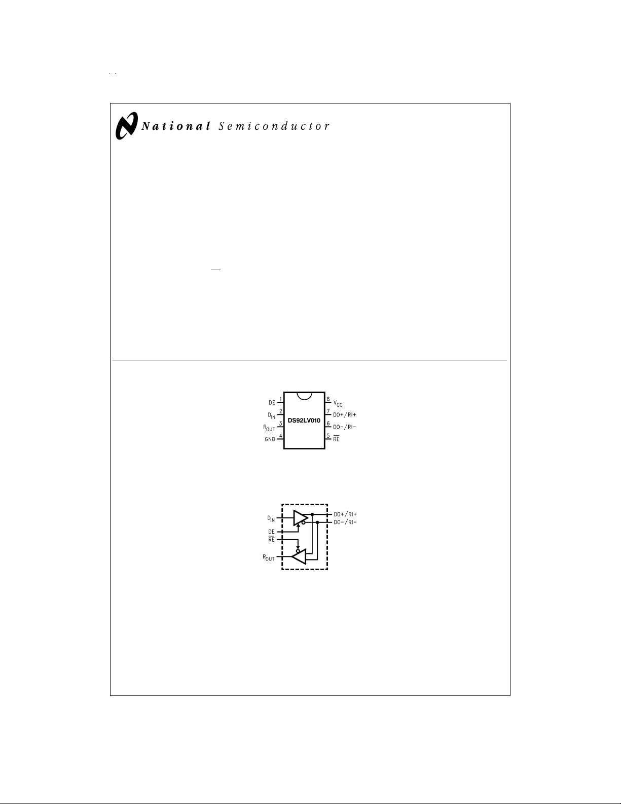
Connection Diagram
The receiver threshold is
mode range and translates the low voltage differential levels
to standard (CMOS/TTL) levels.
Features
n Bus LVDS Signaling (BLVDS)
n Designed for Double Termination Applications
n Balanced Output Impedance
n Lite Bus Loading 5pF typical
n Glitch free power up/down (Driver disabled)
n 3.3V or 5.0V Operation
±
n
1V Common Mode Range
±
n
100mV Receiver Sensitivity
n High Signaling Rate Capability (above 100 Mbps)
n Low Power CMOS design
n Product offered in 8 lead SOIC package
n Industrial Temperature Range Operation
May 1998
±
100mV over a±1V common
DS92LV010A Bus LVDS 3.3/5.0V Single Transceiver
DS100052-1
Order Number DS92LV010ATM
See NS Package Number M08A
Block Diagram
DS100052-2
TRI-STATE®is a registered trademark of National Semiconductor Corporation.
© 1998 National Semiconductor Corporation DS100052 www.national.com
Page 2
Absolute Maximum Ratings (Notes 1, 2)
If Military/Aerospace specified devices are required,
please contact the National Semiconductor Sales Office/
Distributors for availability and specifications.
Supply Voltage (V
Enable Input Voltage (DE,
RE)
Driver Input Voltage (DIN) −0.3V to (V
Receiver Output Voltage
)
(R
OUT
Bus Pin Voltage (DO/RI
Driver Short Circuit
Current
ESD (HBM 1.5 kΩ, 100
pF)
) 6.0V
CC
−0.3V to (VCC+
−0.3V to (V
±
) −0.3V to + 3.9V
Continuous
>
0.3V)
CC
0.3V)
CC
0.3V)
2.0 kV
+
+
SOIC 1025 mW
Derate SOIC Package 8.2 mW/˚C
Storage Temperature
Range
−65˚C to +150˚C
Lead Temperature
(Soldering, 4 sec.) 260˚C
Recommended Operating
Conditions
Min Max Units
Supply Voltage (V
Supply Voltage (V
Receiver Input Voltage 0.0 2.9 V
Operating Free Air
Temperature
), or 3.0 3.6 V
CC
) 4.5 5.5 V
CC
−40 +85 ˚C
Maximum Package Power Dissipation at 25˚C
DC Electrical Characteristics (Notes 2, 3)
TA= −40˚C to +85˚C unless otherwise noted, VCC= 3.3V±0.3V
Symbol Parameter Conditions Pin Min Typ Max Units
V
OD
∆V
OD
V
OS
∆V
OS
I
OSD
V
OH
V
OL
I
OS
V
TH
V
TL
I
IN
V
IH
V
IL
I
IH
I
IL
V
CL
I
CCD
I
CCR
I
CCZ
I
CC
Output Differential
Voltage
VODMagnitude Change 330mV
Offset Voltage 1 1.25 1.65 V
Offset Magnitude
Change
Output Short Circuit
Current
Voltage Output High VID= +100 mV IOH= −400 µA R
Voltage Output Low IOL= 2.0 mA, VID= −100 mV 0.1 0.4 V
Output Short Circuit
Current
Input Threshold High DE = 0V DO+/RI+,
Input Threshold Low −100 mV
Input Current DE = 0V, VIN= +2.4V, or 0V −20
Minimum Input High
Voltage
Maximum Input Low
Voltage
Input High Current VIN=VCCor 2.4V
Input Low Current VIN= GND or 0.4V
Input Diode Clamp
Voltage
Power Supply Current DE = RE = VCC,RL=27Ω V
RL=27Ω,
Figure 1
DO+/RI+,
140 250 360 mV
DO−/RI−
550mV
VO= 0V, DE = V
CC
OUT
−12 −20 mA
2.8 3 V
Inputs Open 2.8 3 V
Inputs Shorted 2.8 3 V
Inputs Terminated,
R
=27Ω
L
V
= 0V, VID= +100 mV −5 −35 −85 mA
OUT
2.8 3 V
+100 mV
DO−/RI−
±
1 +20 µA
V
= 0V, VIN= +2.4V, or 0V −20
CC
DIN, DE,RE2.0 V
±
1 +20 µA
CC
GND 0.8 V
±1±
10 µA
±1±
10 µA
I
= −18 mA −1.5 −0.8 V
CLAMP
CC
13 20 mA
DE=RE=0V 58mA
DE = 0V, RE = V
CC
3 7.5 mA
DE=VCC,RE=0V,RL=27Ω 16 22 mA
V
www.national.com 2
Page 3
DC Electrical Characteristics (Notes 2, 3) (Continued)
TA= −40˚C to +85˚C unless otherwise noted, VCC= 3.3V±0.3V
Symbol Parameter Conditions Pin Min Typ Max Units
C
output
Capacitance@BUS
Pins
DO+/RI+,
DO−/RI−
5pF
DC Electrical Characteristics (Notes 2, 3)
TA= −40˚C to +85˚C unless otherwise noted, VCC= 5.0V±0.5V
Symbol Parameter Conditions Pin Min Typ Max Units
V
OD
∆V
V
OS
∆V
I
OSD
V
OH
V
I
V
V
V
V
I
CCD
I
CCR
I
I
C
output
Note 1: “Absolute Maximum Ratings” are these beyond which the safety of the device cannot be guaranteed. They are not meant to imply that the device should
be operated at these limits. The table of “Electrical Characteristics” provides conditions for actual device operation.
Note 2: All currents into device pins are positive; all currents out of device pins are negative.All voltages are referenced to device ground except V
V
Note 3: All typicals are given for V
Note 4: ESD Rating: HBM (1.5 kΩ, 100 pF)
Note 5: C
Note 6: Generator waveforms for all tests unless otherwise specified: f = 1MHz, ZO = 50Ω,tr,tf≤6.0ns (0%–100%) on control pins and ≤ 1.0ns for RI inputs.
Note 7: The DS92LV010A is a current mode device and only function with datasheet specification when a resistive load is applied between the driver outputs.
Note 8: For receiver TRI-STATE
Output Differential
Voltage
VODMagnitude Change 330mV
OD
Offset Voltage 1 1.35 1.65 V
Offset Magnitude
OS
Change
Output Short Circuit
Current
Voltage Output High VID= +100 mV IOH= −400 µA R
Voltage Output Low IOL= 2.0 mA, VID= −100 mV 0.1 0.4 V
OL
Output Short Circuit
OS
Current
Input Threshold High DE = 0V DO+/RI+,
TH
Input Threshold Low −100 mV
TL
I
Input Current DE = 0V, VIN= +2.4V, or 0V −20
IN
Minimum Input High
IH
Voltage
V
Maximum Input Low
IL
Voltage
Input High Current VIN=VCCor 2.4V
I
IH
I
Input Low Current VIN= GND or 0.4V
IL
Input Diode Clamp
CL
Voltage
Power Supply Current DE = RE = VCC,RL=27Ω V
CCZ
CC
Capacitance@BUS
Pins
unless otherwise specified.
TL
includes probe and fixture capacitance.
L
= +3.3V or 5.0 V and TA= +25˚C, unless otherwise stated.
CC
®
delays, the switch is set to VCCfor t
RL=27Ω,
Figure 1
DO+/RI+,
145 270 390 mV
DO−/RI−
550mV
VO= 0V, DE = V
CC
OUT
−12 −20 mA
4.3 5.0 V
Inputs Open 4.3 5.0 V
Inputs Shorted 4.3 5.0 V
Inputs
Terminated, R
V
= 0V, VID= +100 mV −35 −90 −130 mA
OUT
=27Ω
L
4.3 5.0 V
+100 mV
DO−/RI−
±
1 +20 µA
V
= 0V, VIN= +2.4V, or 0V −20
CC
DIN,
DE,
RE
I
= −18 mA −1.5 −0.8 V
CLAMP
GND 0.8 V
CC
±
1 +20 µA
2.0 V
±1±
±1±
17 25 mA
CC
10 µA
10 µA
DE=RE=0V 610mA
DE = 0V, RE = V
CC
38mA
DE=VCC,RE=0V,RL=27Ω 20 25 mA
DO+/RI+,
5pF
DO−/RI−
OD,VID,VTH
>
2.0 kV EAT (0Ω, 200 pF)>300V.
, and t
PZL
and to GND for t
PLZ
PZH
, and t
PHZ
.
and
V
www.national.com3
Page 4

AC Electrical Characteristics (Note 6)
TA= −40˚C to +85˚C, VCC= 3.3V±0.3V
Symbol Parameter Conditions Min Typ Max Units
DIFFERENTIAL DRIVER TIMING REQUIREMENTS
t
PHLD
t
PLHD
t
SKD
t
TLH
t
THL
t
PHZ
t
PLZ
t
PZH
t
PZL
Differential Prop. Delay High to
Low
RL=27Ω,
CL=10pF
Differential Prop. Delay Low to
High
Differential SKEW |t
PHLD-tPLHD
| 0.2 1.0 ns
Transition Time Low to High 0.3 2.0 ns
Transition Time High to Low 0.3 2.0 ns
Disable Time High to Z RL=27Ω,
Disable Time Low to Z 0.5 5.0 10.0 ns
CL=10pF
Enable Time Z to High 2.0 5.0 7.0 ns
Enable Time Z to Low 1.0 4.5 9.0 ns
DIFFERENTIAL RECEIVER TIMING REQUIREMENTS
t
PHLD
t
PLHD
t
SKD
t
r
t
f
t
PHZ
t
PLZ
t
PZH
t
PZL
Differential Prop. Delay High to
Low
Figures 6, 7
CL=10pF
Differential Prop. Delay Low to
High
Differential SKEW |t
PHLD-tPLHD
| 0.5 2.0 ns
Rise Time 1.5 4.0 ns
Fall Time 1.5 4.0 ns
Disable Time High to Z RL= 500Ω,
Disable Time Low to Z 2.0 5.0 7.0 ns
CL= 10 pF (Note 8)
Enable Time Z to High 2.0 7.0 13.0 ns
Enable Time Z to Low 2.0 6.0 10.0 ns
Figures 2, 3
Figures 4, 5
Figures 8, 9
1.0 3.0 5.0 ns
1.0 2.8 5.0 ns
0.5 4.5 9.0 ns
2.5 5.0 12.0 ns
2.5 5.5 10.0 ns
2.0 4.0 6.0 ns
AC Electrical Characteristics (Note 6)
TA= −40˚C to +85˚C, VCC= 5.0V±0.5V
Symbol Parameter Conditions Min Typ Max Units
DIFFERENTIAL DRIVER TIMING REQUIREMENTS
t
PHLD
t
PLHD
t
SKD
t
TLH
t
THL
t
PHZ
t
PLZ
t
PZH
t
PZL
Differential Prop. Delay High to
Low
RL=27Ω,
CL=10pF
Differential Prop. Delay Low to
High
Differential SKEW |t
PHLD-tPLHD
| 0.2 1.0 ns
Transition Time Low to High 0.3 2.0 ns
Transition Time High to Low 0.3 2.0 ns
Disable Time High to Z RL=27Ω,
Disable Time Low to Z 0.5 5.0 10.0 ns
CL=10pF
Enable Time Z to High 2.0 4.0 7.0 ns
Enable Time Z to Low 1.0 4.0 9.0 ns
DIFFERENTIAL RECEIVER TIMING REQUIREMENTS
t
PHLD
t
PLHD
t
SKD
t
r
t
f
www.national.com 4
Differential Prop. Delay High to
Low
Figures 6, 7
CL=10pF
Differential Prop. Delay Low to
High
Differential SKEW |t
PHLD-tPLHD
| 0.4 2.0 ns
Rise Time 1.2 2.5 ns
Fall Time 1.2 2.5 ns
Figures 2, 3
Figures 4, 5
0.5 2.7 4.5 ns
0.5 2.5 4.5 ns
0.5 3.0 7.0 ns
2.5 5.0 12.0 ns
2.5 4.6 10.0 ns
Page 5

AC Electrical Characteristics (Note 6) (Continued)
TA= −40˚C to +85˚C, VCC= 5.0V±0.5V
Symbol Parameter Conditions Min Typ Max Units
DIFFERENTIAL RECEIVER TIMING REQUIREMENTS
t
PHZ
t
PLZ
t
PZH
t
PZL
Disable Time High to Z RL= 500Ω,
Disable Time Low to Z 2.0 4.0 6.0 ns
CL= 10 pF (Note 8)
Figures 8, 9
Enable Time Z to High 2.0 5.0 9.0 ns
Enable Time Z to Low 2.0 5.0 7.0 ns
2.0 4.0 6.0 ns
Test Circuits and Timing Waveforms
DS100052-3
FIGURE 1. Differential Driver DC Test Circuit
DS100052-4
FIGURE 2. Differential Driver Propagation Delay and Transition Time Test Circuit
DS100052-5
FIGURE 3. Differential Driver Propagation Delay and Transition Time Waveforms
www.national.com5
Page 6

Test Circuits and Timing Waveforms (Continued)
FIGURE 4. Driver TRI-STATE Delay Test Circuit
FIGURE 5. Driver TRI-STATE Delay Waveforms
DS100052-6
DS100052-7
FIGURE 6. Receiver Propagation Delay and Transition Time Test Circuit
FIGURE 7. Receiver Propagation Delay and Transition Time Waveforms
www.national.com 6
DS100052-8
DS100052-9
Page 7

Test Circuits and Timing Waveforms (Continued)
FIGURE 8. Receiver TRI-STATE Delay Test Circuit
FIGURE 9. Receiver TRI-STATE Delay Waveforms TRI-STATE Delay Waveforms
Typical Bus Application Configurations
DS100052-10
DS100052-11
Bi-Directional Half-Duplex Point-to-Point Applications
Multi-Point Bus Applications
Application Information
There are a few common practices which should be implied
when designing PCB for BLVDS signaling. Recommended
practices are:
Use at least 4 layer PCB board (BLVDS signals, ground,
•
power and TTL signals).
DS100052-12
DS100052-13
Keep drivers and receivers as close to the (BLVDS port
•
side) connector as possible.
www.national.com7
Page 8

Use the termination resistor which best matches the dif-
Application Information (Continued)
Bypass each BLVDSdevice and also use distributed bulk
•
capacitance. Surface mount capacitors placed close to
•
ferential impedance of your transmission line.
Leave unused LVDS receiver inputs open (floating)
•
power and ground pins work best. Two or three multilayer ceramic (MLC) surface mount capacitors (0.1 µF,
and 0.01 µFin parallel should be used between each V
and ground. The capacitors should be as close as possible to the V
pin.
CC
CC
TABLE 1. Functional Table
MODE SELECTED DE RE
DRIVER MODE H H
RECEIVER MODE L L
TRI-STATE MODE L H
LOOP BACK MODE H L
TABLE 2. Transmitter Mode
INPUTS OUTPUTS
DE DI DO+ DO−
HL LH
HH HL
>
H2
>
&
0.8 X X
LX ZZ
L = Low state
H = High state
RE
LL(
LH(
L 100 mV
HXZ
X = High or Low logic state
Z = High impedance state
L = Low state
H = High state
TABLE 4. Device Pin Description
Pin Name Pin # Input/Output Description
DIN 2 I TTL Driver Input
±
±
DO
/RI
R
OUT
RE
6, 7 I/O LVDS Driver Outputs/LVDS Receiver Inputs
3 O TTL Receiver Output
5 I Receiver Enable TTL Input (Active Low)
DE 1 I Driver Enable TTL Input (Active High)
GND 4 NA Ground
V
CC
8 NA Power Supply
TABLE 3. Receiver Mode
INPUTS OUTPUT
(RI+)-(RI−)
<
−100 mV) L
>
+100 mV) H
>&>
−100 mV X
www.national.com 8
Page 9

9
Page 10

Physical Dimensions inches (millimeters) unless otherwise noted
Order Number DS92LV010ATM
See NS Package Number M08A
DS92LV010A Bus LVDS 3.3/5.0V Single Transceiver
LIFE SUPPORT POLICY
NATIONAL’S PRODUCTS ARE NOT AUTHORIZED FOR USE AS CRITICAL COMPONENTS IN LIFE SUPPORT DEVICES OR SYSTEMS WITHOUT THE EXPRESS WRITTEN APPROVAL OF THE PRESIDENT OF NATIONAL SEMICONDUCTOR CORPORATION. As used herein:
1. Life support devices or systems are devices or systems which, (a) are intended for surgical implant into
the body, or (b) support or sustain life, and whose failure to perform when properly used in accordance
2. A critical component in any component of a life support
device or system whose failure to perform can be reasonably expected to cause the failure of the life support
device or system, or to affect its safety or effectiveness.
with instructions for use provided in the labeling, can
be reasonably expected to result in a significant injury
to the user.
National Semiconductor
Corporation
Americas
Tel: 1-800-272-9959
Fax: 1-800-737-7018
Email: support@nsc.com
www.national.com
National does not assume any responsibility for use of any circuitry described, no circuit patent licenses are implied and National reserves the right at any time without notice to change said circuitry and specifications.
National Semiconductor
Europe
Fax: +49 (0) 1 80-530 85 86
Email: europe.support@nsc.com
Deutsch Tel: +49 (0) 1 80-530 85 85
English Tel: +49 (0) 1 80-532 78 32
Français Tel: +49 (0) 1 80-532 93 58
Italiano Tel: +49 (0) 1 80-534 16 80
National Semiconductor
Asia Pacific Customer
Response Group
Tel: 65-2544466
Fax: 65-2504466
Email: sea.support@nsc.com
National Semiconductor
Japan Ltd.
Tel: 81-3-5620-6175
Fax: 81-3-5620-6179
 Loading...