

Page 1
Ultra-High-Speed Flash Microcontrollers
DS89C430/DS89C440/DS89C450
www.maxim-ic.com
GENERAL DESCRIPTION
The DS89C430, DS89C440, and DS89C450 offer the
highest performance available in 8051-compatible
microcontrollers. They feature newly designed
processor cores that execute instructions up to 12
times faster than the original 8051 at the same
crystal speed. Typical applications will experience a
speed improvement up to 10x. At 1 million
instructions per second (MIPS) per megahertz, the
microcontrollers achieve 33 MIPS performance from
a maximum 33MHz clock rate.
The Ultra-High-Speed Flash Microcontroller User’s Guide should
be used in conjunction with this data sheet. Download it at
www.maxim-ic.com/microcontrollers
.
FEATURES
§ High-Speed 8051 Architecture
One Clock-Per-Machine Cycle
DC to 33MHz Operation
Single Cycle Instruction in 30ns
Optional Variable Length MOVX to Access
Fast/Slow Peripherals
Dual Data Pointers with Automatic
Increment/Decrement and Toggle Select
Supports Four Paged Memory-Access Modes
§ On-Chip Memory
16kB/32kB/64kB Flash Memory
In-Application Programmable
In-System Programmable Through Serial Port
1kB SRAM for MOVX
APPLICATIONS
Data Logging Vending
Automotive Test Equipment Motor Control
Magstripe Reader/Scanner Consumer Electronics
Gaming Equipment Telephones
HVAC Programmable Logic
Uninterruptible Power
Supplies
Building Energy Control and
Management
White Goods (Washers,
Microwaves, etc.)
Controllers
Building Security and
Door Access Control
Industrial Control and
Automation
ORDERING INFORMATION
PART
DS89C430-MNL
DS89C430-QNL 16kB x 8 44 PLCC
DS89C430-ENL 16kB x 8 44 TQFP
DS89C440-MNL
DS89C440-QNL 32kB x 8 44 PLCC
DS89C440-ENL 32kB x 8 44 TQFP
DS89C450-MNL
DS89C450-QNL 64kB x 8 44 PLCC
DS89C450-ENL 64kB x 8 44 TQFP
Complete Selector Guide appears at end of data sheet.
Pin Configurations appear at end of data sheet.
FLASH
MEMORY SIZE
16kB x 8 40 PDIP
32kB x 8 40 PDIP
64kB x 8 40 PDIP
PIN-PACKAGE
§ 80C52 Compatible
8051 Pin and Instruction Set Compatible
Four Bidirectional, 8-Bit I/O Ports
Three 16-Bit Timer Counters
256 Bytes Scratchpad RAM
§ Power-Management Mode
Programmable Clock Divider
Automatic Hardware and Software Exit
§ ROMSIZE Feature
Selects Internal Program Memory Size from
0 to 64kB
Allows Access to Entire External Memory Map
Dynamically Adjustable by Software
§ Peripheral Features
Two Full-Duplex Serial Ports
Programmable Watchdog Timer
13 Interrupt Sources (Six External)
Five Levels of Interrupt Priority
Power-Fail Reset
Early Warning Power-Fail Interrupt
Electromagnetic Interference (EMI) Reduction
Note: Some revisions of this device may incorporate deviations from published specifications known as errata. Multiple revisions of any device
may be simultaneously available through various sales channels. For information about device errata, click here: www.maxim-ic.com/errata
1 of 48
REV: 111003
.
Page 2

DS89C430/DS89C44/DS89C450 Ultra-High-Speed Flash Microcontrollers
ABSOLUTE MAXIMUM RATINGS
Voltage Range on Any Pin Relative to Ground -0.3V to (VCC + 0.5V)
Voltage Range on V
Relative to Ground -0.3V to +6.0V
CC
Ambient Temperature Range (under bias) -40°C to +85°C
Storage Temperature Range -55°C to +125°C
Soldering Temperature See IPC/JEDEC J-STD-020A
Stresses beyond those listed under “Absolute Maximum Ratings” may cause permanent damage to the device. These are stress ratings only,
and functional operation of the device at these or any other conditions beyond those indicated in the operational sections of the specifications is
not implied. Exposure to the absolute maximum rating conditions for extended periods may affect device reliability.
DC ELECTRICAL CHARACTERISTICS
(VCC = 4.5V to 5.5V, TO = -40°C to +85°C.) (Note 1)
PARAMETER SYMBOL MIN TYP MAX UNITS
Supply Voltage (Notes 2, 3) V
Power-Fail Warning (Notes 2, 4) V
Reset Trip Point (Min Operating Voltage) (Notes 2, 3, 4) V
CC
4.2 4.375 4.6 V
PFW
3.95 4.125 4.35 V
RST
4.5 5.0 5.5 V
Supply Current, Active Mode (Note 5) ICC 75 110 mA
Supply Current, Idle Mode at 33MHz (Note 6) I
Supply Current, Stop Mode, Bandgap Disabled (Note 7) I
Supply Current, Stop Mode, Bandgap Enabled (Note 7) I
40 50 mA
IDLE
1 100 mA
STOP
150 300 mA
SPBG
Input Low Level (Note 2) VIL -0.3 +0.8 V
Input High Level (Note 2) VIH 2.0 VCC + 0.3 V
Input High Level XTAL and RST (Note 2) V
Output Low Voltage, Port 1 and 3 at IOL = 1.6mA (Note 2) V
Output Low Voltage, Port 0 and 2, ALE, PSEN at IOL = 3.2mA
(Note 2)
Output High Voltage, Port 1, 2, and 3, at IOH = -50mA
(Notes 2, 8)
Output High Voltage, Port 1, 2, and 3 at IOH = -1.5mA (Notes 2, 9) V
Output High Voltage, Port 0, 1, 2, ALE, PSEN, RD, WR in Bus
Mode at I
= -8mA (Notes 2, 10)
OH
Output High Voltage, RST at IOL = -0.4mA (Note 2, 11) V
3.5 VCC + 0.3 V
IH2
0.15 0.45 V
OL1
V
0.15 0.45 V
OL2
V
2.4 V
OH1
2.4 V
OH2
V
2.4 V
OH3
2.4 V
OH4
Input Low Current, Port 1, 2, and 3 at 0.4V IIL -50 mA
Transition Current from 1 to 0, Port 1, 2, and 3 at 2V (Note 12) ITL -650 mA
Input Leakage Current, Port 0 in I/O Mode and EA (Note 13) IL -10 +10 mA
Input Current, Port 0 in Bus Mode (Note 14) IL -300 +300 mA
RST Pulldown Resistance (Note 13) R
RST
50 120 200 kW
2 of 48
Page 3

Note 1:
Note 2:
Note 3:
Note 4:
Note 5:
Note 6:
Note 7:
Note 8:
Note 9:
Note 10:
Note 11:
Note 12:
Note 13:
Note 14:
DS89C430/DS89C440/DS89C450 Ultra-High-Speed Flash Microcontrollers
Specifications to -40°C are guaranteed by design and not production tested.
All voltages are referenced to ground.
The user should note that this part is tested and guaranteed to operate down to 4.5V (10%) and that V
that point. This indicates that there is a range of voltages [(V
MIN
to V
(min)] where the processor's operation is not guaranteed, but
RST
the reset trip point has not been reached. This should not be an issue in most applications, but should be considered when proper
operation must be maintained at all times. For these applications, it may be desirable to use a more accurate external reset.
While the specifications for V
PFW
and V
overlap, the design of the hardware makes it so this is not possible. Within the ranges
RST
given, there is guaranteed separation between these two voltages.
Active current is measured with a 33MHz clock source driving XTAL1, V
Idle mode current is measured with a 33MHz clock source driving XTAL1, V
= RST = 5.5V. All other pins are disconnected.
CC
= 5.5V, RST at ground. All other pins are
CC
disconnected.
Stop mode is measured with XTAL and RST grounded, V
= 5.5V. All other pins are disconnected.
CC
RST = 5.5V. This condition mimics the operation of pins in I/O mode.
During a 0-to-1 transition, a one shot drives the ports hard for two clock cycles. This measurement reflects a port pin in transition
mode.
When addressing external memory.
Guaranteed by design.
Ports 1, 2, and 3 source transition current when pulled down externally. The current reaches its maximum at approximately 2V.
RST = 5.5V. Port 0 is floating during reset and when in the logic-high state during I/O mode.
This port is a weak address holding latch in bus mode. Peak current occurs near the input transition point of the holding latch at
approximately 2V.
(min) is specified below
RST
3 of 48
Page 4

AC CHARACTERISTICS
(VCC = 4.5V to 5.5V, TO = -40°C to +85°C.) (See Figure 1, Figure 2, and Figure 3.)
DS89C430/DS89C440/DS89C450
PARAMETER SYMBOL
System Clock External
Oscillator (Note 15)
System Clock External Crystal
(Note 15)
ALE Pulse Width (Note 16) t
Port 0 Instruction Address Valid
to ALE Low
Port 2 Instruction Address Valid
to ALE Low
Port 0 Data AddressValid to
ALE Low
Program Address Hold After
ALE Low
Address Hold after ALE Low
MOVX Write
1-CYCLE
PAGE MODE 1
2-CYCLE
PAGE MODE 1
4-CYCLE
PAGE MODE 1
PAGE MODE 2 NONPAGE MODE
MIN MAX MIN MAX MIN MAX MIN MAX MIN MAX
1/t
0 33 0 33 0 33 0 33 0 33
CLCL
1/t
1 33 1 33 1 33 1 33 1 33
CLCL
0.5t
- 2
LHLL
t
t
AVLL
t
0.5t
AVLL2
t
AVLL3
t
0.5t
LLAX
t
LLAX2
CLCL
+ t
STC3
- 4 0.5t
CLCL
- 8 1.5t
CLCL
0.5t
- 8
CLCL
+ t
STC4
t
- 2
CLCL
+ t
STC3
- 4 1.5t
CLCL
- 8 2.5t
CLCL
1.5t
- 8
CLCL
+ t
STC4
2t
- 4
CLCL
+ t
STC3
- 4 0.5t
CLCL
- 8 1t
CLCL
2.5t
- 8
CLCL
+ t
STC3
1.5t
- 5
CLCL
+ t
STC3
- 3 0.5t
CLCL
- 4 t
CLCL
t
- 3 +
CLCL
t
STC3
- 10 1t
CLCL
0.5t
- 8
CLCL
+ t
STC2
1.5t
CLCL
+ t
STC3
CLCL
- 4
CLCL
0.5t
CLCL
+ t
STC3
- 10
CLCL
0.5t
CLCL
+ t
STC2
- 5
- 3
- 3
- 8
UNITS
MHz
ns
ns
ns
ns
ns
ns
Address Hold after ALE Low
MOVX Read
ALE Low to Valid Instruction In t
ALE Low to PSEN Low t
PSEN Pulse Width for Program
Fetch
0.5t
- 8
t
LLAX3
2t
LLIV
1.5t
LLPL
t
t
PLPH
CLCL
+ t
STC4
- 5 t
CLCL
1.5t
- 8
CLCL
+ t
STC4
- 5 2t
CLCL
2.5t
- 8
CLCL
+ t
STC3
- 5 t
CLCL
0.5t
- 8
CLCL
+ t
STC3
CLCL
- 6 0.5t
CLCL
- 5 2t
CLCL
4 of 48
0.5t
- 8
+ t
CLCL
STC2
- 6 2t
- 2
CLCL
- 5
CLCL
CLCL
- 6
ns
ns
ns
ns
Page 5

AC CHARACTERISTICS (continued)
(VCC = 4.5V to 5.5V, TO = -40°C to +85°C.) (See Figure 1, Figure 2, and Figure 3.)
DS89C430/DS89C440/DS89C450 Ultra-High-Speed Flash Microcontrollers
PARAMETER SYMBOL
PSEN Low to Valid Instruction
In
Input Instruction Hold After
PSEN
Input Instruction Float After
PSEN
Port 0 Address to Valid
Instruction In
Port 2 Address to Valid
Instruction In
PSEN Low to Port 0 Address
Float
RD Pulse Width (P3.7)
(Note 16)
WR Pulse Width (P3.6)
(Note 16)
1-CYCLE
PAGE MODE 1
2-CYCLE
PAGE MODE 1
4-CYCLE
PAGE MODE 1
PAGE MODE 2 NONPAGE MODE
MIN MAX MIN MAX MIN MAX MIN MAX MIN MAX
t
t
PLIV
t
0 0 0 0 0
PXIX
t
t
PXIZ
t
1.5t
AVIV0
t
t
AVIV2
t
0 0
PLAZ
t
- 5
t
RLRH
t
WLWH
CLCL
+ t
STC1
t
- 5
CLCL
+ t
STC1
- 20 t
CLCL
- 20 1.5t
CLCL
t
- 5
+ t
t
+ t
CLCL
CLCL
STC1
- 5
STC1
- 20 2t
CLCL
- 20 2.5t
CLCL
2t
- 5
2t
CLCL
+ t
CLCL
+ t
STC1
STC1
- 5
- 20 t
CLCL
- 20 3t
CLCL
2t
- 5
CLCL
+ t
STC1
2t
- 5
CLCL
+ t
STC1
- 20 2t
CLCL
- 5 t
CLCL
- 22 3t
CLCL
- 20 3.5t
CLCL
2t
- 5
CLCL
+ t
STC1
2t
- 5
CLCL
+ t
STC1
CLCL
CLCL
CLCL
CLCL
- 20
- 5
- 22
- 20
UNITS
ns
ns
ns
ns
ns
ns
ns
ns
RD (P3.7) Low to Valid Data In
(Note 16)
Data Hold After RD (P3.7) t
Data Float After RD (P3.7) t
MOVX ALE Low to Input Data
Valid (Note 16)
t
- 18
t
RLDV
0 0 0 0 0
RHDX
t
RHDZ
t
LLDV
CLCL
+ t
STC1
t
CLCL
+ t
- 18
STC1
2t
- 18
CLCL
+ t
STC1
2t
- 18
CLCL
+ t
STC1
- 5 t
CLCL
2t
- 8
CLCL
+ t
STC1
2t
- 18
2t
CLCL
+ t
CLCL
CLCL
+ t
STC1
- 5
- 5
STC1
5 of 48
ns
ns
ns
ns
Page 6
AC CHARACTERISTICS (continued)
(VCC = 4.5V to 5.5V, TO = -40°C to +85°C.) (See Figure 1, Figure 2, and Figure 3.)
DS89C430/DS89C440/DS89C450 Ultra-High-Speed Flash Microcontrollers
PARAMETER SYMBOL
PAGE MODE 1
1-CYCLE
2-CYCLE
PAGE MODE 1
4-CYCLE
PAGE MODE 1
PAGE MODE 2 NONPAGE MODE
MIN MAX MIN MAX MIN MAX MIN MAX MIN MAX
- 8
- 5
STC2
- 2 t
3t
CLCL
+ t
3.5t
20 + t
0.5t
+ t
STC2
STC1
CLCL
CLCL
STC2
- 20
STC1
+ 5
+ 4
-
Port 0 Address to Valid Data
In (Note 16)
Port 2 Address to Valid Data
In (Note 16)
ALE Low to RD or WR Low
(Note 16)
Port 0 Address Valid to RD or
WR Low (Note 16)
Port 2 Address Valid to RD or
WR Low (Note 16)
Data Out Valid to WR
Transition (Note 15)
Data Hold After WR
(Note 15)
RD or WR High to ALE High
(Note 15)
3t
- 20
t
AVDV0
- 8
- 5
STC2
1.5t
-
CLCL
20 + t
2t
+ 6
CLCL
+ t
STC2
+ 4 t
STC2
STC1
4t
1.5t
t
CLCL
CLCL
+ t
+ t
STC2
STC2
CLCL
STC5
+ t
- 10
- 8
- 2 t
t
- 20
t
AVDV2
t
LLRL
t
LLWL)
(
t
AVRL0
t
AVWL0)
(
t
AVRL2
(t
AVWL2)
t
-5 -5 -5 -5 -5
QVWX
t
WHQX
t
RHLH
t
WHLH)
(
- 8 +
0.5t
CLCL
t
STC2
0 + t
STC5
t
+ t
CLCL
- 10
t
- 2 t
STC2
CLCL
+ t
0.5t
6 + t
- 5
STC2
STC2
STC1
+
CLCL
STC2
+ 4 t
2t
0.5t
t
CLCL
CLCL
+ t
+ t
STC2
STC2
CLCL
STC5
+ t
- 10
- 2 t
- 5
STC2
3.5t
-
CLCL
20 + t
4t
CLCL
t
STC2
STC1
+ 6 +
+ 4 t
STC2
0.5t
1.5t
t
t
CLCL
CLCL
CLCL
+ t
STC2
CLCL
+ t
STC2
- 5 +
t
STC5
+ t
STC2
- 10
- 2 t
STC2
- 8
- 5
CLCL
+ t
STC1
3.0t
- 20
CLCL
+ t
STC1
+ 4
0.5t
CLCL
+ t
STC2
+ 4 t
STC2
0.5t
t
1.5t
t
CLCL
+ t
CLCL
+ t
STC2
CLCL
STC2
- 5 +
t
STC2
CLCL
STC5
+ t
- 10
Note: Specifications to -40°C are guaranteed by design and are not production tested. AC electrical characteristics assume 50% duty cycle for the oscillator and are not 100% tested, but are
guaranteed by design.
UNITS
ns
ns
ns
ns
ns
ns
ns
ns
6 of 48
Page 7
P
R
W
Note 15:
The clock divide and crystal multiplier control bits in the PMR register determine the system clock frequency and the minimum/
maximum external clock speed. The term “1/t
following table. The minimum/maximum external clock speed columns clarify that [(external clock speed) x (multipliers)] cannot
exceed the rated speed of the device. In addition, the use of the crystal multiplier feature establishes a minimum external speed.
4X/2X
CD1 CD0
1 0 0 1 10MHz 8.25MHz
0 0 0 2 5MHz 16.5MHz
X 0 1 Reserved — —
X 1 0 4 See AC Characteristics See AC Characteristics
X 1 1 1/1024 See AC Characteristics See AC Characteristics
Note 16:
Note 17:
External MOVX instruction times are dependent upon the setting of the MD2, MD1, and MD0 bits in the clock control register. The
, t
, t
terms “t
STC1
STC2
” used in the variable timing table above are calculated through the use of the table given below.
STC3
MD2 MD1 MD0 MOVX Instruction Time t
0 0 0 2 Machine Cycles 0 t
0 0 1 3 Machine Cycles 2 t
0 1 0 4 Machine Cycles 6 t
0 1 1 5 Machine Cycles 10 t
1 0 0 6 Machine Cycles 14 t
1 0 1 7 Machine Cycles 18 t
1 1 0 8 Machine Cycles 22 t
1 1 1 9 Machine Cycles 26 t
Maximum load capacitance (to meet the above timing) for Port 0, ALE, PSEN, WR, and RD is limited to 60pF. XTAL1 and XTAL2 load
capacitance are dependent upon the frequency of the selected crystal.
Figure 1. Nonpage Mode Timing
XTAL1
t
CLCL
ALE
t
AVLL2
t
SEN
AVLL
” used in the AC Characteristics variable timing table is determined from the
CLCL
Number of External Clock
Cycles per System Clock
(1/t
)
CLCL
t
LHLL
t
AVLL3
t
t
STC1
0 t
CLCL
1 t
CLCL
1 t
CLCL
1 t
CLCL
5 t
CLCL
5 t
CLCL
5 t
CLCL
5 t
CLCL
LLAX3
DS89C430/DS89C440/DS89C450
External Clock Speed
Min Max
t
STC2
0 t
CLCL
0 t
CLCL
0 t
CLCL
0 t
CLCL
4 t
CLCL
4 t
CLCL
4 t
CLCL
4 t
CLCL
t
STC3
0 t
CLCL
0 t
CLCL
0 t
CLCL
0 t
CLCL
1 t
CLCL
1 t
CLCL
1 t
CLCL
1 t
CLCL
t
STC4
0 t
CLCL
1 t
CLCL
1 t
CLCL
1 t
CLCL
1 t
CLCL
1 t
CLCL
1 t
CLCL
1 t
CLCL
t
LLAX2
STC5
CLCL
CLCL
CLCL
CLCL
CLCL
CLCL
CLCL
CLCL
D
R
Port 0
Port 2
LSB
t
LLIV
t
LLPL
t
PXIX
t
LLAX
MOVX MOVX
t
PXIZ
t
AVIV0
t
PLPH
t
AVWL2
t
PLIV
t
RLRH
t
LLDV
t
AVDV0
t
RLDV
LSBLSB LSB LSB
t
AVDV2
DATA
t
RHDX
t
t
AVIV2
RHDZ
t
PLAZ
t
AVWL0
OPCODE
t
t
WHQX
MSB MSBMSBMSB MSB
7 of 48
WHLH
t
LLWL
t
WLWH
t
QVWX
DATA
Page 8
Figure 2. Page Mode 1 Timing
P
R
W
P
R
W
XTAL1
CLCL
t
ALE
AVLL2
t
SEN
D
R
AVIV2
t
Port 0
OPCODE
MOVX
MOVX
DS89C430/DS89C440/DS89C450 Ultra-High-Speed Flash Microcontrollers
LHLL
t
PLPH
t
LLAX2
LLAX3
t
LLWL
t
RLRH
t
RHDX
t
RLDV
t
DATA
AVDV2
t
LLAX
t
PXIX
t
PLIV
t
OPCODE
t
QVWX
t
AVWL2
t
DATA
WHLH
t
WHQX
t
WLWH
t
Port 2
LSB
LSB LSB LSB
Figure 3. Page Mode 2 Timing
XTAL1
t
CLCL
ALE
t
AVLL
t
AVLL2
SEN
D
R
Port 0
Port 2
MSB
t
LLPL
t
PLIV
t
AVIV0
t
PXIX
t
LLIV
t
t
LLAX
OPCODE DATA
MOVX MOVX
PXIZ
t
PLPH
MSB LSB MSBMSB MSB LSB
t
LHLL
t
t
AVLL3
LLAX2
t
t
t
AVDV0
t
AVDV2
t
LLDV
t
RLRH
AVWL2
LLAX3
t
RLDV
t
PLAZ
t
RHDX
t
RHDZ
MSB
t
AVIV2
LSBLSB LSB LSBLSB
t
AVWL0
OPCODE
t
WLWH
t
WHLH
t
LLWL
t
WHQX
LSB
t
QVWX
MSB MSB
DATA
8 of 48
Page 9

DS89C430/DS89C440/DS89C450 Ultra-High-Speed Flash Microcontrollers
EXTERNAL CLOCK CHARACTERISTICS
(V
= 4.5V to 5.5V, TO = -40°C to +85°C.)
CC
PARAMETER SYMBOL MIN MAX UNITS
Clock High Time t
Clock Low Time t
Clock Rise Time t
Clock Fall Time t
10 ns
CHCX
10 ns
CLCX
5 ns
CLCH
5 ns
CHCL
SERIAL PORT MODE 0 TIMING CHARACTERISTICS
(V
= 4.5V to 5.5V, TO = -40°C to +85°C.) (Figure 4)
CC
PARAMETER SYMBOL CONDITIONS
SM2 = 0 360 12t
Clock Cycle Time t
XLXL
SM2 = 1 120 4t
Output Data Setup to Clock
Rising
t
QVXH
SM2 = 0 200
SM2 = 1 40 3t
Output Data Hold to Clock
Rising
t
XHQX
SM2 = 0 50 2t
SM2 = 1 20 t
33MHz VARIABLE
MIN MAX MIN MAX
ns
CLCL
ns
CLCL
10t
-
CLCL
100
- 10 ns
CLCL
- 10 ns
CLCL
- 100
CLCL
UNITS
ns
Input Data Hold After Clock
Rising
Clock Rising Edge to Input
Data Valid
Note: SM2 is the serial port 0 mode bit 2. When serial port 0 is operating in mode 0 (SM0 = SM1 = 0), SM2 determines the number of crystal
clocks in a serial port clock cycle.
t
XHDX
t
XHDV
SM2 = 0 0 0 ns
SM2 = 1 0 0
SM2 = 0 200 10t
- 100 ns
CLCL
SM2 = 1 40 3t
- 50 ns
CLCL
9 of 48
Page 10
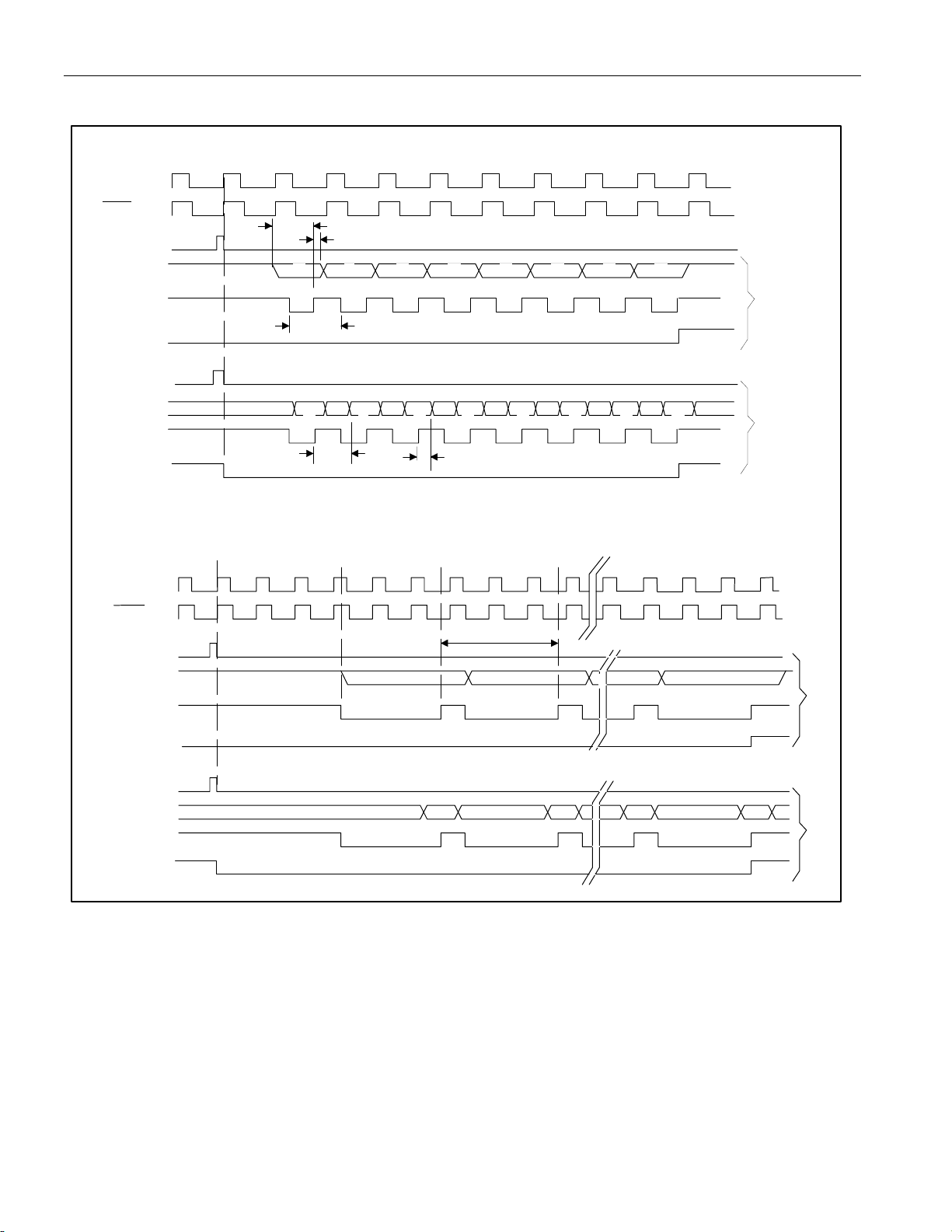
Figure 4. Serial Port Timing
SERIAL PORT (SYNCHRONOUS MODE)
SM2 = 1 TDX CLOCK = XTAL FREQ/4
ALE
DS89C430/DS89C440/DS89C450 Ultra-High-Speed Flash Microcontrollers
PSEN
WRITE TO SBUF
RXD DATA OUT
TXD CLOCK
TI
WRITE TO SCON
TO CLEAR RI
RXD DATA IN
TXD CLOCK
R1
t
QVXH
D0 DI D3 D4D2 D5 D6 D7
t
XLXL
t
XHDV
SERIAL PORT (SYNCHRONOUS MODE)
SM2 = 0 TDX CLOCK = XTAL FREQ/12
ALE
PSEN
WRITE TO SBUF
RXD DATA OUT
TXD CLOCK
t
XHQX
D7D6D5D4D3D2DID0
t
XHDX
1/(XTAL FREQ/12)
D0 DI D6 D7
TRANSMIT
RECEIVE
T
R
A
N
S
M
I
T
WRITE TO SCON
TXD CLOCK
TO CLEAR RI
RXD DATA IN
TXD CLOCK
TI
R1
D0 DI D6 D7
10 of 48
R
E
C
E
I
V
E
Page 11
DS89C430/DS89C440/DS89C450 Ultra-High-Speed Flash Microcontrollers
POWER-CYCLE TIMING CHARACTERISTICS
(VCC = 4.5V to 5.5V, TO = -40°C to +85°C.)
PARAMETER SYMBOL MIN TYP MAX UNITS
Crystal Startup Time (Note 18) t
Power-On Reset Delay (Note 19)
Note 18: Startup time for a crystal varies with load capacitance and manufacturer. The time shown is for an 11.0592MHz crystal manufactured
Note 19: Reset delay is a synchronous counter of crystal oscillations after crystal startup. Counting begins when the level on the XTAL1 pin
by Fox Electronics.
meets the V
criteria. At 33MHz, this time is 1.99ms.
IH2
8 ms
CSU
65,536 t
t
POR
CLCL
FLASH MEMORY PROGRAMMING CHARACTERISTICS
(VCC = 4.5V to 5.5V)
PARAMETER SYMBOL MIN TYP MAX UNITS
Data Retention (Note 20) tDR 100 years
Write/Erase Endurance t
Program/Time t
Erase Time t
Note 20: At room temperature.
20,000 cycles
ENDURE
40 ms
PROG
4 ms
ERASE
11 of 48
Page 12
PIN DESCRIPTION
DS89C430/DS89C440/DS89C450 Ultra-High-Speed Flash Microcontrollers
PIN
PDIP PLCC TQFP
40 12, 44 6, 38 VCC
1, 22, 23,
20
9 10 4 RST
19 21 15 XTAL1
18 20 14 XTAL2
29 32 26
30 33 27
39 43 37 P0.0 (AD0)
38 42 36 P0.1 (AD1)
37 41 35 P0.2 (AD2)
36 40 34 P0.3 (AD3)
35 39 33 P0.4 (AD4)
34 38 32 P0.5 (AD5)
33 37 31
32 36 30
34
16, 17, 28,
39
NAME FUNCTION
GND
PSEN
ALE/PROG
P0.6 (AD6)
P0.7 (AD7)
+5V
Logic Ground
External Reset. The RST input pin is bidirectional and contains a Schmitt Trigger to
recognize external active-high reset inputs. The pin also employs an internal pulldown
resistor to allow for a combination of wire-ORed external reset sources. An RC is not
required for power-up, as the device provides this function internally.
Crystal Oscillators. These pins provide support for fundamental-mode parallel-resonant
AT-cut crystals. XTAL1 also acts as an input if there is an external clock source in place of
a crystal. XTAL2 serves as the output of the crystal amplifier.
Program Store Enable. This signal is commonly connected to optional external program
memory as a chip enable. PSEN provides an active-low pulse and is driven high when
external program memory is not being accessed. In one-cycle page mode 1, PSEN
remains low for consecutive page hits.
Address Latch Enable. This signal functions as a clock to latch the external address LSB
from the multiplexed address/data bus on Port 0. This signal is commonly connected to the
latch enable of an external 373-family transparent latch. In default mode, ALE has a pulse
width of 1.5 XTAL1 cycles and a period of four XTAL1 cycles. In page mode, the ALE
pulse width is altered according to the page mode selection. In traditional 8051 mode, ALE
is high when using the EMI reduction mode and during a reset condition. ALE can be
enabled by writing ALEON = 1 (PMR.2). Note that ALE operates independently of ALEON
during external memory accesses. As an alternate mode, this pin (PROG) is used to
execute the parallel program function.
Port 0 (AD0–AD7), I/O. Port 0 is an open-drain, 8-bit, bidirectional I/O port. As an
alternate function, Port 0 can function as the multiplexed address/data bus to access offchip memory. During the time when ALE is high, the LSB of a memory address is
presented. When ALE falls to logic 0, the port transitions to a bidirectional data bus. This
bus is used to read external program memory and read/write external RAM or peripherals.
When used as a memory bus, the port provides weak pullups for logic 1 outputs. The reset
condition of port 0 is tri-state. Pullup resistors are required only when using port 0 as an
I/O port.
12 of 48
Page 13

DS89C430/DS89C440/DS89C450 Ultra-High-Speed Flash Microcontrollers
PIN DESCRIPTION (continued)
PIN
PDIP PLCC TQFP
1 2 40 P1.0
2 3 41 P1.1
3 4 42 P1.2
4 5 43 P1.3
5 6 44 P1.4
6 7 1 P1.5
7 8 2 P1.6
8 9 3 P1.7
21 24 18 P2.0 (A8)
22 25 19 P2.1 (A9)
23 26 20 P2.2(A10)
24 27 21 P2.3(A11)
25 28 22 P2.4(A12)
26 29 23 P2.5(A13)
27 30 24 P2.6(A14)
28 31 25 P2.7(A15)
10 11 5 P3.0
11 13 7 P3.1
12 14 8 P3.2
13 15 9 P3.3
14 16 10 P3.4
15 17 11 P3.5
16 18 12 P3.6
17 19 13 P3.7
NAME FUNCTION
Port 1, I/O. Port 1 functions as both an 8-bit, bidirectional I/O port and an alternate
functional interface for timer 2 I/O, new external interrupts, and new serial port 1. The
reset condition of port 1 is with all bits at logic 1. In this state, a weak pullup holds the port
high. This condition also serves as an input state, since any external circuit that writes to
the port overcomes the weak pullup. When software writes a 0 to any port pin, the
DS89C430/DS89C440/DS89C450 activate a strong pulldown that remains on until either
a 1 is written or a reset occurs. Writing a 1 after the port has been at 0 causes a strong
transition driver to turn on, followed by a weaker sustaining pullup. Once the momentary
strong driver turns off, the port again becomes the output high (and input) state. The
alternate functions of port 1 are as follows:
PORT ALTERNATE FUNCTION
P1.0 T2 External I/O for Timer/Counter2
P1.1 T2EX Timer 2 Capture/Reload Trigger
P1.2 RXD1 Serial Port 1 Receive
P1.3 TXD1 Serial Port 1 Transmit
P1.4 INT2 External Interrupt 2 (Positive Edge Detect)
P1.5 INT3 External Interrupt 3 (Negative Edge Detect)
P1.6 INT4 External Interrupt 4 (Positive Edge Detect)
P1.7 INT5 External Interrupt 5 (Negative Edge Detect)
Port 2 (A8–A15), I/O. Port 2 is an 8-bit, bidirectional I/O port. The reset condition of port 2
is logic high. In this state, a weak pullup holds the port high. This condition also serves as
an input mode, since any external circuit that writes to the port overcomes the weak
pullup. When software writes a 0 to any port pin, the DS89C430/DS89C440/DS89C450
activate a strong pulldown that remains on until either a 1 is written or a reset occurs.
Writing a 1 after the port has been at 0 causes a strong transition driver to turn on,
followed by a weaker sustaining pullup. Once the momentary strong driver turns off, the
port again becomes both the output high and input state. As an alternate function, port 2
can function as the MSB of the external address bus when reading external program
memory and read/write external RAM or peripherals. In page mode 1, port 2 provides both
the MSB and LSB of the external address bus. In page mode 2, it provides the MSB and
data.
Port 3, I/O. Port 3 functions as both an 8-bit, bidirectional I/O port and an alternate
functional interface for external interrupts, serial port 0, timer 0 and 1 inputs, and RD and
WR strobes. The reset condition of port 3 is with all bits at a logic 1. In this state, a weak
pullup holds the port high. This condition also serves as an input mode, since any external
circuit that writes to the port overcomes the weak pullup. When software writes a 0 to any
port pin, the DS89C430/DS89C440/DS89C450 activate a strong pulldown that remains on
until either a 1 is written or a reset occurs. Writing a 1 after the port has been at 0 causes
a strong transition driver to turn on, followed by a weaker sustaining pullup. Once the
momentary strong driver turns off, the port again becomes both the output high and input
state. The alternate modes of port 3 are as follows:
PORT ALTERNATE FUNCTION
P3.0 RXD0 Serial Port 0 Receive
P3.1 TXD0 Serial Port 0 Transmit
P3.2 INT0 External Interrupt 0
P3.3 INT1 External Interrupt 1
P3.4 T0 Timer 0 External Input
P3.5 T1 Timer 1 External Input
P3.6 WR External Data Memory Write Strobe
P3.7 RD External Data Memory Read Strobe
31 35 29
EA
External Access. Allows selection of internal or external program memory. Connect to
ground to force the DS89C430/DS89C440/DS89C450 to use an external memory program
memory. The internal RAM is still accessible as determined by register settings. Connect
to use internal flash memory.
to V
CC
13 of 48
Page 14
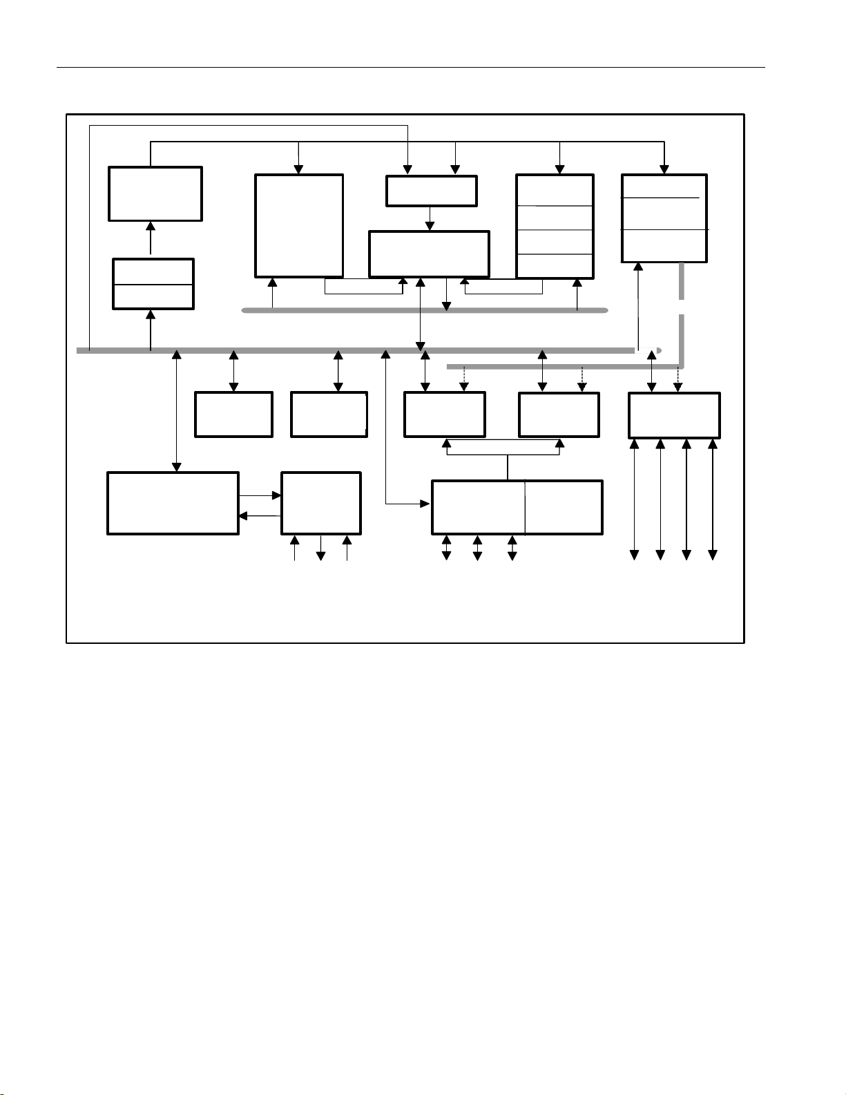
Figure 5. Functional Diagram
P
E
DS89C430/DS89C440/DS89C450 Ultra-High-Speed Flash Microcontrollers
CONTROL
AND
SEQUENCER
DECODER
IR
INTERNAL CONTROL BUS
SERIAL I/O
WATCHDOG TIMER
AND
POWER MANAGER
Dallas Semiconductor
DS89C430/DS89C440/
DS89C450
INTERNAL
REGISTERS
TIMER/
COUNTERS
CLOCK
AND
RESET
XTAL2
XTAL1
INTERRUPT
CPU
1kB x 8
RAM
MEMORY
CONTROL
A
RST
SEN
SFRs
DPTR
DPTR1
SP
16kB/32kB
64kB x 8
FLASH
ROM
LOADER
PROG
PC
AR INC
AR
ADDRESS BUS
I/O PORTS
P0 P1
P2 P3
ALE/
DETAILED DESCRIPTION
The DS89C430, DS89C440, and DS89C450 are pin compatible with all three packages of the standard 8051 and
include standard resources such as three timer/counters, serial port, and four 8-bit I/O ports. The three part
numbers vary only by the amount of internal flash memory (DS89C430 = 16kB, DS89C440 = 32kB, DS89C450 =
64kB), which can be in-system/in-application programmed from a serial port using ROM-resident or user-defined
loader software. For volume deployments, the flash can also be loaded externally using standard commercially
available parallel programmers.
Besides greater speed, the DS89C430/DS89C440/DS89C450 include 1kB of data RAM, a second full hardware
serial port, seven additional interrupts, two extra levels of interrupt priority, programmable watchdog timer,
brownout monitor, and power-fail reset. Dual data pointers (DPTRs) are included to speed up block data-memory
moves with further enhancements coming from selectable automatic increment/decrement and toggle select
operation. The speed of MOVX data memory access can be adjusted by adding stretch values up to 10 machine
cycles for flexibility in selecting external memory and peripherals.
A power management mode consumes significantly lower power by slowing the CPU execution rate from one clock
period per cycle to 1024 clock periods per cycle. A selectable switchback feature can automatically cancel this
mode to enable normal speed responses to interrupts.
For EMI-sensitive applications, the microcontroller can disable the ALE signal when the processor is not accessing
external memory.
14 of 48
Page 15

DS89C430/DS89C440/DS89C450 Ultra-High-Speed Flash Microcontrollers
Terminology
The term DS89C430 is used in the remainder of the document to refer to the DS89C430, DS89C440, and
DS89C450, unless otherwise specified.
Compatibility
The DS89C430 is a fully static CMOS 8051-compatible microcontroller similar in functional features to the
DS87C520, but it offers much higher performance. In most cases, the DS89C430 can drop into an existing socket
for the 8xC51 family, immediately improving the operation. While remaining familiar to 8051 family users, the
DS89C430 has many new features. In general, software written for existing 8051-based systems works without
modification on the DS89C430, with the exception of critical timing routines, as the DS89C430 performs its
instructions much faster for any given crystal selection.
The DS89C430 provides three 16-bit timer/counters, two full-duplex serial ports, and 256 bytes of direct RAM plus
1kB of extra MOVX RAM. I/O ports can operate as in standard 8051 products. Timers default to 12 clocks-percycle operation to keep their timing compatible with a legacy 8051 family systems. However, timers are individually
programmable to run at the new one clock per cycle if desired. The DS89C430 provides several new hardware
features, described in subsequent sections, implemented by new special-function registers (SFRs).
Performance Overview
Featuring a completely redesigned high-speed 8051-compatible core, the DS89C430 allows operation at a higher
clock frequency. This updated core does not have the wasted memory cycles that are present in a standard 8051.
A conventional 8051 generates machine cycles using the clock frequency divided by 12. The same machine cycle
takes one clock in the DS89C430. Thus, the fastest instructions execute 12 times faster for the same crystal
frequency (and actually 24 times faster for the INC data pointer instruction). It should be noted that this speed
improvement is reduced when using external memory access modes that require more than one clock per cycle.
Individual program improvement depends on the instructions used. Speed-sensitive applications would make the
most use of instructions that are 12 times faster. However, the sheer number of 12-to-1 improved op codes makes
dramatic speed improvements likely for any code. These architectural improvements produce instruction cycle
times as low as 30ns. The dual data pointer feature also allows the user to eliminate wasted instructions when
moving blocks of memory. The new page modes allow for increased efficiency in external memory accesses.
Instruction Set Summary
All instructions have the same functionality as their 8051 counterparts, including their affect on bits, flags, and other
status functions. However, the timing of each instruction is different, in both absolute and relative number of clocks.
For absolute timing of real-time events, the duration of software loops can be calculated using information given in
the Instruction Set table in the Ultra-High-Speed Flash Microcontroller User’s Guide. However, counter/timers
default to run at the older 12 clocks per increment. In this way, timer-based events occur at the standard intervals
with software executing at higher speed. Timers optionally can run at a reduced number of clocks per increment to
take advantage of faster processor operation.
The relative time of some instructions may be different in the new architecture. For example, in the original
architecture, the “MOVX A, @DPTR” instruction and the “MOV direct, direct” instruction used two machine cycles
or 24 oscillator cycles. Therefore, they required the same amount of time. In the DS89C430, the MOVX instruction
takes as little as two machine cycles or two oscillator cycles, but the “MOV direct, direct” uses three machine cycles
or three oscillator cycles. While both are faster than their original counterparts, they now have different execution
times. This is because the DS89C430 usually uses one machine cycle for each instruction byte and requires one
cycle for execution. The user concerned with precise program timing should examine the timing of each instruction
to become familiar with the changes.
Special-Function Registers (SFRs)
All peripherals and operations that are not explicit instructions in the DS89C430 are controlled through SFRs. The
most common features basic to the architecture are mapped to the SFRs. These include the CPU registers (ACC,
B, and PSW), data pointers, stack pointer, I/O ports, timer/counters, and serial ports. In many cases, an SFR
controls an individual function or reports the function’s status. The SFRs reside in register locations 80h–FFh and
are only accessible by direct addressing. SFRs with addresses ending in 0h or 8h are bit addressable.
15 of 48
Page 16

DS89C430/DS89C440/DS89C450 Ultra-High-Speed Flash Microcontrollers
All standard SFR locations from the 8051 are duplicated in the DS89C430, and several SFRs have been added for
the unique features of the DS89C430. Most of these features are controlled by bits in SFRs located in unused
locations in the 8051 SFR map, allowing for increased functionality while maintaining complete instruction set
compatibility. Table 1
shows the SFRs and their locations. Table 2 specifies the default reset condition for all SFR
bits.
Data Pointers
The data pointers (DPTR and DPTR1) are used to assign a memory address for the MOVX instructions. This
address can point to a MOVX RAM location (on-chip or off-chip) or a memory-mapped peripheral. Two pointers are
useful when moving data from one memory area to another, or when using a memory-mapped peripheral for both
source and destination addresses. The user can select the active pointer through a dedicated SFR bit (SEL =
DPS.0), or can activate an automatic toggling feature for altering the pointer selection (TSL = DPS.5). An additional
feature, if selected, provides automatic incrementing or decrementing of the current DPTR.
Stack Pointer
The stack pointer denotes the register location at the top of the stack, which is the last used value. The user can
place the stack anywhere in the scratchpad RAM by setting the stack pointer to the desired location, although the
lower bytes are normally used for working registers.
I/O Ports
The DS89C430 offers four 8-bit I/O ports. Each I/O port is represented by an SFR location and can be written or
read. The I/O port has a latch that contains the value written by software.
Counter/Timers
Three 16-bit timer/counters are available in the DS89C430. Each timer is contained in two SFR locations that can
be read or written by software. The timers are controlled by other SFRs, described in the SFR Bit Description
section of the Ultra-High-Speed Flash Microcontroller User’s Guide.
Serial Ports
The DS89C430 provides two UARTs that are controlled and accessed by SFRs. Each UART has an address that
is used to read and write the value contained in the UART. The same address is used for both read and write
operations, and the read and write operations are distinguished by the instruction. Its own SFR control register
controls each UART.
Table 1. SFR Register Map
REGISTER ADDRESS BIT 7 BIT 6 BIT 5 BIT 4 BIT 3 BIT 2 BIT 1 BIT 0
P0 80h P0.7 P0.6 P0.5 P0.4 P0.3 P0.2 P0.1 P0.0
SP 81h
DPL 82h
DPH 83h
DPL1 84h
DPH1 85h
DPS 86h ID1 ID0 TSL AID — — — SEL
PCON 87h SMOD_0 SMOD0 OFDF OFDE GF1 GF0 STOP IDLE
TCON 88h TF1 TR1 TF0 TR0 IE1 IT1 IE0 IT0
TMOD 89h GATE C/T M1 M0 GATE C/T M1 M0
TL0 8Ah
TL1 8Bh
TH0 8Ch
16 of 48
Page 17

DS89C430/DS89C440/DS89C450 Ultra-High-Speed Flash Microcontrollers
Table 1. SFR Register Map (continued)
REGISTER ADDRESS BIT 7 BIT 6 BIT 5 BIT 4 BIT 3 BIT 2 BIT 1 BIT 0
TH1 8Dh
CKCON 8Eh WD1 WD0 T2M T1M T0M MD2 MD1 MD0
P1 90h P1.7/INT5 P1.6/INT4 P1.5/INT3 P1.4/INT2 P1.3/TXD1 P1.2/RXD1 P1.1/T2EX P1.0/T2
EXIF 91h IE5 IE4 IE3 IE2 CKRY RGMD RGSL BGS
CKMOD 96h T2MH T1MH T0MH — — —
SCON0 98h SM0/FE_0 SM1_0 SM2_0 REN_0 TB8_0 RB8_0 TI_0 RI_0
SBUF0 99h
ACON 9Dh PAGEE PAGES1 PAGES0 —
P2 A0h P2.7 P2.6 P2.5 P2.4 P2.3 P2.2 P2.1 P2.0
IE A8h EA ES1 ET2 ES0 ET1 EX1 ET0 EX0
SADDR0 A9h
SADDR1 AAh
P3 B0h P3.7/RD P3.6/WR P3.5/T1 P3.4/T0 P3.3/INT1 P3.2/INT0 P3.1/TXD0 P3.0/RXD0
IP1 B1h — MPS1 MPT2 MPS0 MPT1 MPX1 MPT0 MPX0
IP0 B8h — LPS1 LPT2 LPS0 LPT1 LPX1 LPT0 LPX0
SADEN0 B9h
SADEN1 BAh
SCON1 C0h SM0/FE_1 SM1_1 SM2_1 REN_1 TB8_1 RB8_1 TI_1 RI_1
SBUF1 C1h
ROMSIZE C2h PRAME RMS2 RMS1 RMS0
PMR C4h CD1 CD0 SWB CTM 4X/2X ALEON DME1 DME0
STATUS C5h PIS2 PIS1 PIS0 — SPTA1 SPRA1 SPTA0 SPRA0
TA C7h
T2CON C8h TF2 EXF2 RCLK TCLK EXEN2 TR2 C/T2 CP/RL2
T2MOD C9h T2OE DCEN
RCAP2L CAh
RCAP2H CBh
TL2 CCh
TH2 CDh
PSW D0h CY AC F0 RS1 RS0 OV F1 P
FCNTL D5h FBUSY FERR FC3 FC2 FC1 FC0
FDATA D6h
WDCON D8h SMOD_1 POR EPFI PFI WDIF WTRF EWT RWT
ACC E0h
EIE E8h — — — EWDI EX5 EX4 EX3 EX2
B F0h
EIP1 F1h — — — MPWDI MPX5 MPX4 MPX3 MPX2
EIP0 F8h — — — LPWDI LPX5 LPX4 LPX3 LPX2
Note: Shaded bits are timed-access protected.
— — — —
17 of 48
Page 18

DS89C430/DS89C440/DS89C450 Ultra-High-Speed Flash Microcontrollers
Table 2. SFR Reset Value
REGISTER ADDRESS BIT 7 BIT 6 BIT 5 BIT 4 BIT 3 BIT 2 BIT 1 BIT 0
P0 80h 1 1 1 1 1 1 1 1
SP 81h 0 0 0 0 0 1 1 1
DPL 82h 0 0 0 0 0 0 0 0
DPH 83h 0 0 0 0 0 0 0 0
DPL1 84h 0 0 0 0 0 0 0 0
DPH1 85h 0 0 0 0 0 0 0 0
DPS 86h 0 0 0 0 0 1 0 0
PCON 87h 0 0 Special Special 0 0 0 0
TCON 88h 0 0 0 0 0 0 0 0
TMOD 89h 0 0 0 0 0 0 0 0
TL0 8Ah 0 0 0 0 0 0 0 0
TL1 8Bh 0 0 0 0 0 0 0 0
TH0 8Ch 0 0 0 0 0 0 0 0
TH1 8Dh 0 0 0 0 0 0 0 0
CKCON 8Eh 0 0 0 0 0 0 0 1
P1 90h 1 1 1 1 1 1 1 1
EXIF 91h 0 0 0 0 Special Special Special 0
CKMOD 96h 1 1 0 0 0 1 1 1
SCON0 98h 0 0 0 0 0 0 0 0
SBUF0 99h 0 0 0 0 0 0 0 0
ACON 9Dh 0 0 0 1 1 1 1 1
P2 A0h 1 1 1 1 1 1 1 1
IE A8h 0 0 0 0 0 0 0 0
SADDR0 A9h 0 0 0 0 0 0 0 0
SADDR1 AAh 0 0 0 0 0 0 0 0
P3 B0h 1 1 1 1 1 1 1 1
IP1 B1h 1 0 0 0 0 0 0 0
IP0 B8h 1 0 0 0 0 0 0 0
SADEN0 B9h 0 0 0 0 0 0 0 0
SADEN1 BAh 0 0 0 0 0 0 0 0
SCON1 C0h 0 0 0 0 0 0 0 0
SBUF1 C1h 0 0 0 0 0 0 0 0
ROMSIZE C2h 1 1 1 1 0 1 0 1
PMR C4h 1 0 0 0 0 0 0 0
STATUS C5h 0 0 0 1 0 0 0 0
TA C7h 1 1 1 1 1 1 1 1
T2CON C8h 0 0 0 0 0 0 0 0
T2MOD C9h 1 1 1 1 1 1 0 0
RCAP2L CAh 0 0 0 0 0 0 0 0
RCAP2H CBh 0 0 0 0 0 0 0 0
18 of 48
Page 19

DS89C430/DS89C440/DS89C450 Ultra-High-Speed Flash Microcontrollers
Table 2. SFR Reset Value (continued)
REGISTER ADDRESS BIT 7 BIT 6 BIT 5 BIT 4 BIT 3 BIT 2 BIT 1 BIT 0
TL2 CCh 0 0 0 0 0 0 0 0
TH2 CDh 0 0 0 0 0 0 0 0
PSW D0h 0 0 0 0 0 0 0 0
FCNTL D5h 1 0 1 1 0 0 0 0
FDATA D6h 0 0 0 0 0 0 0 0
WDCON D8h 0 Special 0 Special 0 Special Special 0
ACC E0h 0 0 0 0 0 0 0 0
EIE E8h 1 1 1 0 0 0 0 0
B F0h 0 0 0 0 0 0 0 0
EIP1 F1h 1 1 1 0 0 0 0 0
EIP0 F8h 1 1 1 0 0 0 0 0
Note: Consult the Ultra-High-Speed Flash Microcontroller User’s Guide for more information about the bits marked “Special.”
Memory Organization
There are three distinct memory areas in the DS89C430: scratchpad registers, program memory, and data
memory. The registers are located on-chip but the program and data memory spaces can be on-chip, off-chip, or
both. The DS89C430/DS89C440/DS89C450 have 16kB/32kB/64kB of on-chip program memory, respectively,
implemented in flash memory and also have 1kB of on-chip data memory space that can be configured as program
space using the PRAME bit in the ROMSIZE feature. The DS89C430 uses a memory-addressing scheme that
separates program memory from data memory. The program and data segments can be overlapped since they are
accessed in different manners. If the maximum address of on-chip program or data memory is exceeded, the
DS89C430 performs an external memory access using the expanded memory bus. The
PSEN signal goes active
low to serve as a chip enable or output enable when performing a code fetch from external program memory.
MOVX instructions activate the
RD or WR signal for external MOVX data memory access. The program memory
ROMSIZE feature allows software to dynamically configure the maximum address of on-chip program memory.
This allows the DS89C430 to act as a bootloader for an external memory. It also enables the use of the
overlapping external program spaces. The lower 128 bytes of on-chip flash memory—if ROMSIZE is greater than
0—are used to store reset and interrupt vectors. 256 bytes of on-chip RAM serve as a register area and program
stack, which are separated from the data memory.
Register Space
Registers are located in the 256 bytes of on-chip RAM labeled “internal registers” (Figure 6), which can be divided
into two sub areas of 128 bytes each. Separate classes of instructions are used to access the registers and the
program/data memory. The upper 128 bytes are overlapped with the 128 bytes of SFRs in the memory map.
Indirect addressing is used to access the upper 128 bytes of scratchpad RAM, while the SFR area is accessed
using direct addressing. The lower 128 bytes can be accessed using direct or indirect addressing.
There are four banks of eight working registers in the lower 128 bytes of scratchpad RAM. The working registers
are general-purpose RAM locations that can be addressed within the selected bank by any instructions that use
R0–R7. The register bank selection is controlled through the program status register in the SFR area. The contents
of the working registers can be used for indirect addressing of the upper 128 bytes of scratchpad RAM.
Individually addressable bits in the RAM and SFR areas support Boolean operations. In the scratchpad RAM area,
registers 20h–2Fh are bit addressable by software using Boolean operation instructions.
Another use of the scratchpad RAM area is for the stack. The stack pointer, contained in the SFRs, is used to
select storage locations for program variables and for return addresses of control operations.
19 of 48
Page 20

DS89C430/DS89C440/DS89C450 Ultra-High-Speed Flash Microcontrollers
Figure 6. Memory Map (as shown for the DS89C430)
FF
80
7F
2F
Bit Addressable
20
1F
00
INTERNAL
REGISTERS
128 Bytes SFR
128 Bytes
Indirect
Addressing
Bank 3
Bank 2
Bank 1
Bank 0
03FF
0000
3FFF
2000
1FFF
0000
INTERNAL
MEMORY
1K x 8
SRAM
Data OR
prog mem
addr from
400 - 7FF
8K x 8
Flash
Memory
(Program)
8K x 8
Flash
Memory
(Program)
FFFF
4000
External
Program
Memory
FFFF
External
Data
Memory
03FF
00000000
Memory Configuration
As illustrated in Figure 6, the DS89C430 incorporates two 8kB flash areas for on-chip program memory and 1kB of
SRAM for on-chip data memory or a particular range (400–7FF) of “alternate” program memory space. The
DS89C440 incorporates two 16kB flash memories and the DS89C450 incorporates two 32kB flash memories. The
DS89C430 uses an address scheme that separates program memory from data memory such that the 16-bit
address bus can address each memory area up to maximum of 64kB.
20 of 48
Page 21

DS89C430/DS89C440/DS89C450 Ultra-High-Speed Flash Microcontrollers
Program Memory Access
On-chip program memory begins at address 0000h and is contiguous through 3FFFh (16kB) on the DS89C430,
through 7FFFh (32kB) on the DS89C440, and through FFFFh (64kB) on the DS89C450. Exceeding the maximum
address of on-chip program memory causes the device to access off-chip memory. The maximum on-chip decoded
address is selectable by software using the ROMSIZE feature. Software can cause the DS89C430 to behave like a
device with less on-chip memory. This is beneficial when overlapping external memory is used. The maximum
memory size is dynamically variable. Thus a portion of memory can be removed from the memory map to access
off-chip memory and then be restored to access on-chip memory. In fact, all the on-chip memory can be removed
from the memory map allowing the full 64kB memory space to be addressed from off-chip memory. Program
memory addresses that are larger than the selected maximum are automatically fetched from outside the part
through ports 0 and 2. Figure 6
The ROMSIZE register is used to select the maximum on-chip decoded address for program memory. Bits RMS2,
RMS1, and RMS0 have the following effect:
RMS2 RMS1 RMS0
0 0 0 0kB
0 0 1 1kB/03FFh
0 1 0 2kB/07FFh
0 1 1 4kB/0FFFh
1 0 0 8kB/1FFFh
1 0 1 16kB/3FFFh (DS89C430 default)
1 1 0 32kB/7FFFh (DS89C440 default)
1 1 1 64kB/FFFFh (DS89C450 default)
shows a depiction of the memory map.
Maximum On-Chip Program Memory
Address (Size/Address)
The reset default condition for all devices is to their maximum on-chip program memory size. When accessing
external program memory, that amount of external memory would be inaccessible. To select a smaller effective
program memory size, software must alter bits RMS2–RMS0. Altering these bits requires a timed-access
procedure, as explained later.
Care should be taken so that changing the ROMSIZE register does not corrupt program execution. For example,
assume that a DS89C430 is executing instructions from internal program memory near the 12kB boundary
(~3000h) and that the ROMSIZE register is currently configured for a 16kB internal program space. If software
reconfigures the ROMSIZE register to 4kB (0000h–0FFFh) in the current state, the device immediately jumps to
external program execution because program code from 4kB to 16kB (1000h–3FFFh) is no longer located on-chip.
This could result in code misalignment and execution of an invalid instruction. The recommended method is to
modify the ROMSIZE register from a location in memory that is internal (or external) both before and after the
operation. In the above example, the instruction that modifies the ROMSIZE register should be located below the
4kB (1000h) boundary or above the 16kB (3FFFh) boundary so that it is unaffected by the memory modification.
The same precaution should be applied if the internal program memory size is modified while executing from
external program memory.
For nonpage mode operations, off-chip memory is accessed using the multiplexed address/data bus on P0 and the
MSB address on P2. While serving as a memory bus, these pins are not I/O ports. This convention follows the
standard 8051 method of expanding on-chip memory. Off-chip program memory access also occurs if the
a logic 0.
EA overrides all ROMSIZE bit settings. The PSEN signal goes active (low) to serve as a chip enable or
EA pin is
output enable when ports 0 and 2 fetch from external program memory.
RD and WR signals are used to control the external data memory device. Data memory is accessed by MOVX
The
instructions. The MOVX@Ri instruction uses the value in the designated working register to provide the LSB of the
address, while port 2 supplies the address MSB. The MOVX@DPTR instruction uses one of the two data pointers
to move data over the entire 64kB external data memory space. Software selects the data pointer used by writing
to the SEL bit (DPS.0).
The DS89C430 also provides a user option for high-speed external memory access by reconfiguring the external
memory interface into page mode operation.
Note: When using the original 8051 expanded bus structure, the throughput is reduced by 75% compared with that
of internal operations. This is because of the CPU being stalled for three out of four clocks, waiting for the data
21 of 48
Page 22

DS89C430/DS89C440/DS89C450 Ultra-High-Speed Flash Microcontrollers
fetch that takes four clocks. Page mode 1 is the only external addressing mode where the CPU does not require
stalls for external memory access, but page misses result in reduced external access performance.
On-Chip Program Memory
The processor can fetch the entire on-chip program memory range automatically. By default, the reset routines and
all interrupt vectors are located in the lower 128 bytes of the on-chip program memory.
On-chip program memory is logically divided into pairs of 8kB, 16kB, or 32kB flash memory banks to support inapplication programming. The on-chip program memory is designed to be programmed in-application with the
standard 5V V
supply under the control of the user software or by using a built-in program memory loader. It can
CC
also be programmed in standard flash or EPROM programmers. The DS89C430 incorporates a memory
management unit (MMU) and other hardware to support any of the three programming methods. The MMU controls
program and data memory access, and provides sequencing and timing controls for programming of the on-chip
program memory. A separate security flash block supports a standard three-level lock, a 64-byte encryption array,
and other flash options.
Security Features
The DS89C430 incorporates a 64-byte encryption array, allowing the user to verify program codes while viewing
the data in encrypted form. The encryption array is implemented in a security flash memory block that has the
same electrical and timing characteristics as the on-chip program memory. Once the encryption array is
programmed to non-FFh, the data presented in the verify mode is encrypted. Each byte of data is XNORed with a
byte in the encryption array during verification.
A three-level lock restricts viewing of the internal program and data memory contents. By programming the three
lock bits, the user can select a level of security as specified in Table 3
.
Once a security level is selected and programmed, the setting of the lock bits remains. Only a mass erase can
erase these bits and allow reprogramming the security level to a less restricted protection.
Table 3. Flash Memory Lock Bits
LEVEL LB1 LB2 LB3 PROTECTION
1 1 1 1 No program lock. Encrypted verify if encryption array is programmed.
Prevent MOVC in external memory from reading program code in internal
2 0 1 1
3 X 0 1
4 X X 0 Level 3 plus no external execution.
The DS89C430 provides user-selectable options that must be set before beginning software execution. The option
control register uses flash bits rather than SFRs, and is individually erasable and programmable as a byte-wide
register. Bit 3 of this register is defined as the watchdog POR. Setting this bit to 1 disables the watchdog reset
function on power-up. Clearing this bit to 0 enables the watchdog reset function automatically. Other bits of this
register are undefined and are at logic 1 when read. The value of this register can be read at address FCh in
parallel programming mode or executing a verify-option-control register instruction in ROM loader mode or inapplication programming mode.
memory. EA is sampled and latched on reset. Allow no further parallel or
program memory loader programming.
Level 2 plus no verify operation. Also prevent MOVX in external memory
from reading internal SRAM.
The signature bytes can be read in ROM loader mode or in parallel programming mode. Reading data from
addresses 30h, 31h, and 60h provides signature information on manufacturer, part, and extension as follows:
ADDRESS VALUE MEANING
30h DAh Manufacturer ID
31h 43h DS89C430 Device ID
31h 44h DS89C440 Device ID
31h 45h DS89C450 Device ID
60h 01h Device Extension
22 of 48
Page 23

DS89C430/DS89C440/DS89C450 Ultra-High-Speed Flash Microcontrollers
Note: The read/write accessibility of the flash memory during in-application programming is not affected by the
state of the lock bits. However, the lock bits do affect the read/write accessibility in ROM loader and parallel
programming modes.
In-Application Programming by User Software
The DS89C430 supports in-application programming of on-chip flash memory by user software. In-application
programming is initiated by writing a flash command into the flash control (FCNTL:D5h) register to enable the flash
memory for erase/program/verify operations. Address and data are input into the MMU through the flash data
(FDATA:D6h) register. The flash command also enables read/write accesses to the FDATA. The MMU’s sequencer
provides the operation sequences and control functions to the flash memory. The MMU is designed to operate
independently from the processor, except for read/write access to the SFRs.
Only the upper bank of the on-chip program memory can be in-application programmed by the user software. The
lower bank of the on-chip program memory contains system hardware-dependent codes that are crucial to system
operation and should not be altered during in-application programming.
All flash operations are self-timed. The user software can monitor the progress of an erase or programming
operation through the flash busy (FBUSY;FCNTL.7) bit with a reset value at logic 1. A selected operation
automatically starts when required data is written to the FDATA SFR. The MMU clears the FBUSY bit to indicate
the start of a write/erase operation. The FBUSY bit may not change state for up to 1ms after the operation is
requested. During this time, the application should poll the status of the FBUSY bit waiting for it to change state.
This bit is held low until either the end of the operation or until an error indicator is returned. A flash operating
failure terminates the current operation and sets the flash error flag (FERR;FCNTL.6) to logic 1. Both the busy and
error flags are read-only bits.
Read/write access during in-application programming is not affected by the state of the lock bits.
The flash command (FC3–FC0;FCNTL.3:0) bits provide flash commands as listed in Table 4
.
23 of 48
Page 24

DS89C430/DS89C440/DS89C450 Ultra-High-Speed Flash Microcontrollers
Table 4. In-Application Programming Commands
FC3:FC0 COMMAND OPERATION
Default state. All flash blocks are in read mode. Note: The upper bank
0000 Read Mode
0001 Verify Option Control Register
0010 Verify Security Block
0011
0100 Reserved for Future Use This command should not be modified by user programs.
1000 Reserved for Future Use This command should not be modified by user programs.
Verify Upper Program
Memory Bank
of flash memory is inaccessible for execution unless the FC3:0 bits are
in the read mode (0000b) state.
Read data from the option control register. Data is available in the
FDATA at the end of the following machine cycle. FDATA.3 is the logic
value of the watchdog POR default setting.
Read a byte of data from the security block. After the address byte is
written to the FDATA, data is available in the FDATA at the end of the
following machine cycle. (Lock bits are addressed at 40h and
FDATA.5:3 are the logic value of LB1, LB2 and LB3, respectively.)
Read a byte of data from upper flash memory bank (address range
from 2000h to 3FFFh). The first and second byte writes to the FDATA
are the upper and lower byte of the address. Data is available in the
FDATA at the end of the following machine cycle after the second
address byte is written.
1001 Write Option Control Register
1010 Write Security Block
1011
1100 Erase Option Control Register
1101 Erase Security Block
1110
1111 System Reset This command is used to cause a system reset.
Write Upper Program
Memory Bank
Erase Upper Program
Memory Bank
Write to the option control register as data is written to FDATA. Bit 3 of
the data byte represents the watchdog POR default setting.
Write a byte of data to the security block at a selected locations
addressed by the first byte write to the FDATA. The second write to the
FDATA is the data byte. (Lock bits are addressed at 40h and the
FDATA 5:3 represents lock bits LB3, LB2, and LB1, respectively.)
Write a byte of code to the upper flash memory bank (address range
from 2000h to 3FFFh). The first and second byte writes to the FDATA
are the upper byte and the lower byte of the address. The third write to
the FDATA is the data byte.
Erase the option control register. The contents of this register are
returned to FFh. This operation disables the watchdog reset function on
power-up.
Erase the security flash block that contains the 64-byte encryption array
and the lock bits. The content of every memory location is turned into
FFh.
Erase the upper bank of flash memory bank. The contents of every
memory location are returned to FFh.
The flash command bits are cleared to 0 on all forms of reset, and it is important for the user software to clear
these bits to 0 to return the flash memory to read mode from erase/program operation. This setting is a “no
operation” condition for the MMU, which allows the processor to return to its normal execution. Note that the busy
and error flags have no function in normal flash-read mode.
The FCNTL SFR can only be written using timed access. This procedure provides protection against inadvertent
erase/program operation on the flash memory. Any command written to the FCNTL during a flash operation is
ignored (FBUSY = 0). To ensure data integrity, an erase command sequence should be reinitiated if an erase or
program operation is interrupted by a reset.
24 of 48
Page 25

DS89C430/DS89C440/DS89C450 Ultra-High-Speed Flash Microcontrollers
ROM Loader
The full on-chip flash program memory space, security flash block, and external SRAM can be programmed insystem from an external source through serial port 0 under the control of a built-in ROM loader. The ROM loader
also has an auto-baud feature that determines which baud-rate frequencies are being used for communication and
sets the baud-rate generator for that speed.
When the DS89C430 is powered up and has entered its user operating mode, the ROM loader mode can be
invoked at any time by forcing RST = 1,
condition (RST = 1 and
PSEN = EA = 0) is removed. Entering the ROM loader mode forces the processor to start
fetching from the 2kB internal ROM for program memory initialization and other loader functions.
The read/write accessibility is determined by the state of the lock bits, which can be verified directly by the ROM
loader.
The flash memory can be programmed (by the built-in ROM loader) using commands that are received over the
serial interface from a host PC. Full details of the ROM loader commands are given in the Ultra-High-Speed Flash
Microcontroller User’s Guide. Host software to communicate with the ROM loader is available in Windows
as well as other platforms. Contact our technical support department at micro.support@dalsemi.com
information.
EA = 0, and PSEN = 0. It remains in effect until power-down or when the
®
format
for more
25 of 48
Page 26

DS89C430/DS89C440/DS89C450 Ultra-High-Speed Flash Microcontrollers
Table 5. Parallel Programming Instruction Set
INSTRUCTION P2.5:0, P1.7:0 P0.7:0
Mass Erase Don’t care Don’t care PL1 H L L L
Write Program
Memory
Read Program
Memory
Write Encryption
Array
Write LB1 Don’t care Don’t care PL2 H H H H Program LB1 to logic 0
Write LB2 Don’t care Don’t care PL2 H H L L Program LB2 and LB1 to 00b
Write LB3 Don’t care Don’t care PL2 H L H L Program LB3, LB2, and LB1 to 000b
Read Lock Bits Don’t care DOUT H3 L L L H
Write Option
Control Register
Erase Option
Control Register
Read Address
30, 31, 60, FC
ADDR DIN PL
ADDR DOUT H
ADDR DIN PL
Don’t care DIN PL
Don’t care Don’t care PL
ADDR DOUT H
PROG
P2.6 P2.7 P3.6 P3.7 OPERATION
Mass erase the program memory and the
security block. The contents of every memory
location is returned to FFh.
2
L H H H Program the program memory
3
L L H H Verify the program memory
2
L H L H Program the encryption array
Verify the lock bits. The lock bits are at
address 40h and the three LSBs of the DOUT
are the logic value of the lock bits LB3, LB2,
and LB1, respectively.
4
L H L L
4
H L L H
3
L L L L
Program the option control register. Bit 3 of
the DIN represents the watchdog POR default
setting.
Erase the option control register. This
operation disables the watchdog reset
function on power-up.
30h = Manufacturer ID
31h = Device ID
60h = Device extension
FCh = Verify the option control register. Bit 3
of the DOUT is the logic value of the
watchdog POR .
Note 1: Mass erase requires an active-low PROG pulse width of 828ms.
Note 2: The byte program requires an active-low PROG pulse width of 100ms (max).
Note 3: PROG is weakly pulled to a high internally.
Note 4: The erase-option control register requires an active-low PROG pulse width of 828ms.
On-Chip MOVX Data Memory
On-chip data memory is provided by the 1kB SRAM and occupies addresses 0000h–03FFh. The internal data
memory is disabled after a power-on reset, and any MOVX instruction directs the data memory access to external
data memory. To enable the internal data memory, software must configure the data memory enable bits DME1
and DME0 (PMR.1–0). Refer to the SFR Bit Descriptions section of the Ultra-High-Speed Flash Microcontroller
User’s Guide for data memory configurations. Once enabled, MOVX instructions with addresses inside the 1kB
range access the on-chip data memory, and addresses exceeding the 1kB range automatically access external
data memory. An internal data memory cycle spans only one system clock period to support fast internal execution.
Data Pointer Increment/Decrement and Options
The DS89C430 incorporates a hardware feature to assist applications that require data pointer increment/
decrement. Data pointer increment/decrement bits ID0 and ID1 (DPS.6 and DPS.7) define how the INC DPTR
instruction functions in relation to the active DPTR (selected by the SEL bit). Setting ID0 = 1 and SEL = 0 enables
the decrement operation for DPTR, and execution of the INC DPTR instruction decrements the DPTR contents
by 1. Similarly, setting ID1 = 1 and SEL = 1 enables the decrement operation for DPTR1, and execution of the INC
26 of 48
Page 27

DS89C430/DS89C440/DS89C450 Ultra-High-Speed Flash Microcontrollers
DPTR instruction decrements the DPTR1 contents by 1. With this feature, the user can configure the data pointers
to operate in four ways for the INC DPTR instruction:
ID1 ID0 SEL = 0 SEL = 1
0 0
0 1
1 0
1 1
INC DPTR INC DPTR1
DEC DPTR INC DPTR1
INC DPTR DEC DPTR1
DEC DPTR DEC DPTR1
SEL (DPS.0) bit always selects the active data pointer. The DS89C430 offers a programmable option that allows
any instructions related to data pointer to toggle the SEL bit automatically. This option is enabled by setting the
toggle-select-enable bit (TSL–DPS.5) to a logic 1. Once enabled, the SEL bit is automatically toggled after the
execution of one of the following five DPTR-related instructions:
INC DPTR
MOV DPTR #data16
MOVC A, @A+DPTR
MOVX A, @DPTR
MOVX @DPTR, A
The DS89C430 also offers a programmable option that automatically increases (or decreases) the contents of the
selected data pointer by 1 after the execution of a DPTR-related instruction. The actual function (increment or
decrement) is dependent on the setting of the ID1 and ID0 bits. This option is enabled by setting the automatic
increment/decrement enable (AID–DPS.4) to a logic 1 and is affected by the following three instructions:
MOVC A, @A+DPTR
MOVX A, @DPTR
MOVX @DPTR, A
External Memory
The DS89C430 executes external memory cycles for code fetches and read/writes of external program and data
memory. A nonpage external memory cycle is four times slower than the internal memory cycles (i.e., an external
memory cycle contains four system clocks). However, a page mode external memory cycle can be completed in
one, two, or four system clocks for a page hit and two, four, or eight system clocks for a page miss, depending on
user selection. The DS89C430 also supports a second page mode operation with a different external bus structure
that provides for fast external code fetches but uses four system clock cycles for data memory access.
External Program Memory Interface (Nonpage Mode)
Figure 7 shows the timing relationship for internal and external code fetches when CD1 and CD0 are set to 10b,
assuming the microcontroller is in nonpage mode for external fetches. Note that an external program fetch takes
four system clocks, and an internal program fetch requires only one system clock.
As illustrated in Figure 7
programmable user option to turn on ALE during internal program memory operation. ALE is automatically enabled
for code fetch externally, independent of the setting of this option.
PSEN is only asserted for external code fetches, and is inactive during internal execution.
, ALE is deasserted when executing an internal memory fetch. The DS89C430 provides a
27 of 48
Page 28

DS89C430/DS89C440/DS89C450 Ultra-High-Speed Flash Microcontrollers
P
Figure 7. External Program Memory Access (Nonpage Mode, CD1:CD0 = 10)
XTAL1
ALE
SEN
Port 0
Internal Memory Cycles
External Memory Cycle
C1
C2 C3 C4 C1 C2 C3 C4
LSB Add Data LSB Add Data
External Memory Cycle
Port 2
MSB Add MSB Add
External Data Memory Interface in Nonpage Mode Operation
Just like the program memory cycle, the external data memory cycle is four times slower than the internal data
memory cycle in nonpage mode. A basic internal memory cycle contains one system clock and a basic external
memory cycle contains four system clocks for nonpage mode operation.
The DS89C430 allows software to adjust the speed of external data memory access by stretching the memory bus
cycle. CKCON (8Eh) provides an application-selectable stretch value for this purpose. Software can change the
stretch value dynamically by changing the setting of CKCON.2–CKCON.0. Table 6
shows the data memory cycle
stretch values and their effect on the external MOVX memory bus cycle and the control signal pulse width in terms
of the number of oscillator clocks. A stretch machine cycle always contains four system clocks.
Table 6. Data Memory Cycle Stretch Values
MD2:MD0
000 0 0.5 1 2 2048
001 1 1 2 4 4096
010 2 2 4 8 8192
011 3 3 6 12 12,288
100 7 4 8 16 16,384
101 8 5 10 20 20,480
110 9 6 12 24 24,576
111 10 7 14 28 28,672
STRETCH
CYCLES
As Table 6
shows, the stretch feature supports eight stretched external data memory access cycles, which can be
categorized into three timing groups. When the stretch value is cleared to 000b, there is no stretch on external data
memory access and a MOVX instruction is completed in two basic memory cycles. When the stretch value is set to
1, 2, or 3, the external data memory access is extended by 1, 2, or 3 stretch machine cycles, respectively. Note
that the first stretch value does not result in adding four system clocks to the
because the first stretch uses one system clock to create additional setup time and one system clock to create
additional address hold time. When using very slow RAM and peripherals, a larger stretch value (4–7) can be
selected. In this stretch category, one stretch machine cycle (4 system clocks) is used to stretch the ALE pulse
width, one stretch machine cycle is used to create additional setup, one stretch machine cycle is used to create
additional hold time, and one stretch machine cycle is added to the
RD/WR PULSE WIDTH (IN NUMBER OF OSCILLATOR CLOCKS)
4X/2X, CD1,
CD0 = 100
4X/2X, CD1,
CD0 = 000
4X/2X, CD1,
CD0 = X10
RD/WR control signals. This is
RD or WR strobes.
4X/2X, CD1,
CD0 = X11
28 of 48
Page 29

DS89C430/DS89C440/DS89C450 Ultra-High-Speed Flash Microcontrollers
PSEN
R
R
PSEN
R
R
The following diagrams illustrate the timing relationship for external data memory access in full speed (stretch value
= 0), in the default stretch setting (stretch value = 1), and slow data memory accessing (stretch value = 4), when
the system clock is in divide-by-1 mode (CD1:CD0 = 10b).
Figure 8. Nonpage Mode, External Data Memory Access (Stretch = 0, CD1:CD2 = 10)
MOVX Instruction
1st Machine Cycle
XTAL1
ALE
D/W
2nd Machine Cycle
Port 0
Port 2
MOVX
Instruction
Fetch
MOVX INSTA DATAA A
AA
Memory
Access
Stretch = 0
Figure 9. Nonpage Mode, External Data Memory Access (Stretch = 1, CD1:CD2 = 10)
MOVX Instruction
XTAL1
ALE
D/W
Port 0
1st Machine Cycle 2nd Machine Cycle
MOVX IN STA DATAA A
3rd Machine Cycle
Port 2
MOVX
Instruction
Fetch
AA
Memory Access
Stretch = 1
29 of 48
Page 30
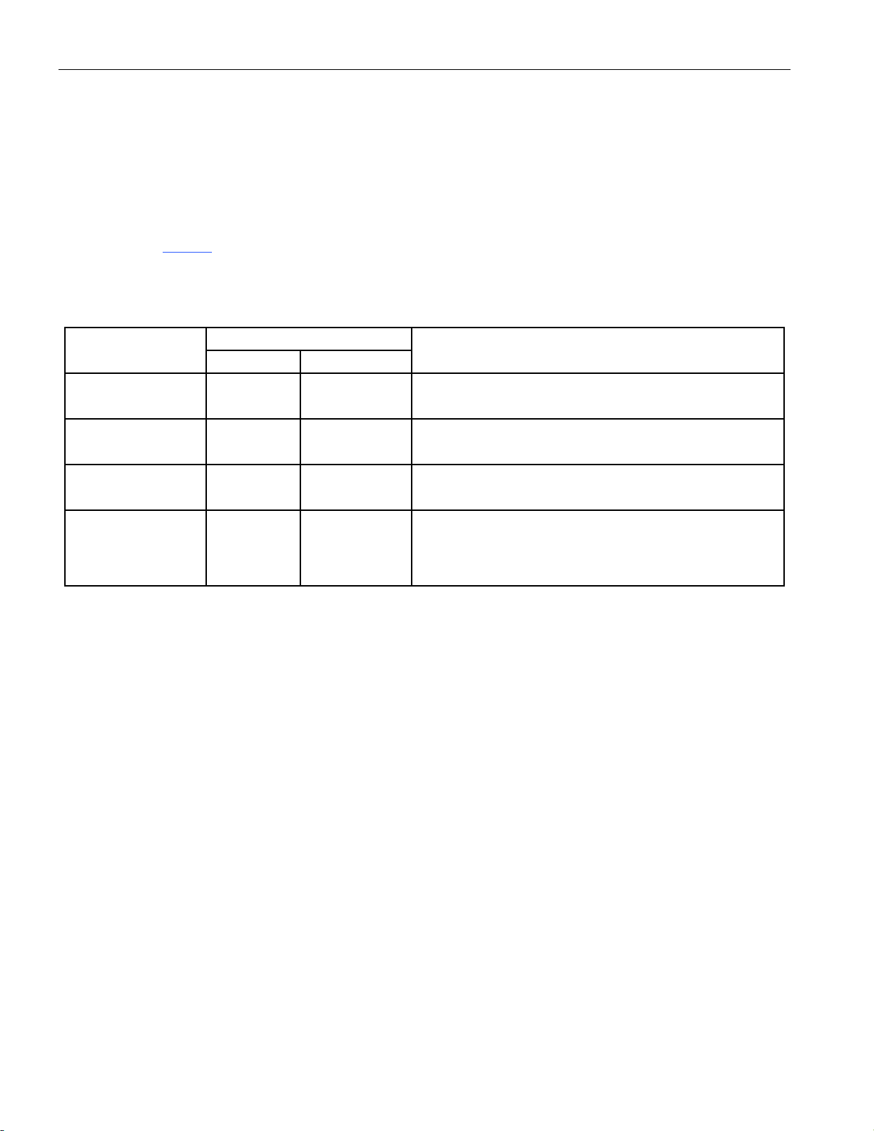
DS89C430/DS89C440/DS89C450 Ultra-High-Speed Flash Microcontrollers
Page Mode, External Memory Cycle
Page mode retains the basic circuitry requirement for an original 8051 external memory interface, but alters the
configuration of P0 and P2 for the purposes of address output and data I/O during external memory cycles.
Additionally, the functions of ALE and
PSEN are altered to support this mode of operation.
Setting the PAGEE (ACON.7) bit to logic 1 enables page mode. Clearing the PAGEE bit to logic 0 disables the
page mode and the external bus structure defaults to the original 8051 expanded bus configuration (nonpage
mode). The DS89C430 supports page mode in two external bus structures. The logic value of the page-modeselect bits in the ACON register determines the external bus structure and the basic memory cycle in number of
system clocks. Table 7
summarizes this option. The first three selections use the same bus structure but with
different memory cycle time. Setting the select bits to 11b selects another bus structure. Write access to the ACON
register requires a timed access.
Table 7. Page Mode Select
PAGES1:PAGES0
00 1 2
01 2 4
10 4 8
11 2 4
CLOCKS PER MEMORY CYCLE
PAGE-HIT PAGE-MISS
EXTERNAL BUS STRUCTURE
P0: Primary data bus.
P2: Primary address bus, multiplexing both the upper byte and
lower byte of address.
P0: Primary data bus.
P2: Primary address bus, multiplexing both the upper byte and
lower byte of address.
P0: Primary data bus.
P2: Primary address bus, multiplexing both the upper byte and
lower byte of address.
P0: Lower address byte.
P2: The upper address byte is multiplexed with the data byte.
Note: This setting affects external code fetches only; accessing
the external data memory requires four clock cycles, regardless
of page hit or miss.
The first page mode’s (page mode 1) external bus structure uses P2 as the primary address bus, (multiplexing both
the most significant byte and least significant byte of the address for each external memory cycle) and P0 is used
as the primary data bus. During external code fetches, P0 is held in a high-impedance state by the processor. Op
codes are driven by the external memory onto P0 and latched at the end of the external fetch cycle at the rising
edge of
PSEN. During external data read/write operations, P0 functions as the data I/O bus. It is held in a high-
impedance state for external reads from data memory and driven with data during external writes to data memory.
§ A page miss occurs when the most significant byte of the subsequent address is different from the last
address. The external memory machine cycle can be 2, 4, or 8 system clocks in length for a page miss.
§ A page hit occurs when the most significant byte of the subsequent address does not change from the last
address. The external memory machine cycle can be 1, 2, or 4 system clocks in length for a page hit.
During a page hit, P2 drives Addr [0–7] of the 16-bit address, while the most significant address byte is held in the
external address latches.
PSEN, RD, and WR strobes accordingly for the appropriate operation on the P0 data bus.
There is no ALE assertion for page hits.
30 of 48
Page 31

DS89C430/DS89C440/DS89C450 Ultra-High-Speed Flash Microcontrollers
PSEN
PSEN
R
R
RD/WR
RD/WR
PSEN
Figure 10. Page Mode 1, External Memory Cycle (CD1:CD0 = 10)
Internal Memory Cycles
XTAL1
ALE
Port 0
Inst
External Memory Cycles
MOVX MOVX
Inst Inst
PAGES=00
Data Data
Port 2
ALE
D/W
Port 0
Port 2
ALE
Port 0
LSB
MOVX
MSBAdd LSB Add LSB Add MSBAdd MSBAdd LSB Add
Page Miss Page Miss Data AccessPage Hit
MSB MSB MSB MSB MSB LSB LSB LSB LSB LSB LSB
Inst
MOVX executed
Page MissPage HitPage Miss Data Access Data Access
MOVX executedMOVX executed
Inst
PAGES=01
Data
next instruction
PAGES=10
Data
Port 2
MSBAdd LSB Add LSB Add
Page Miss Data Access
During a page miss, P2 drives the Addr [8:15] of the 16-bit address and holds it for the duration of the first half of
the memory cycle to allow the external address latches to latch the new most significant address byte. ALE is
asserted to strobe the external address latches. During this operation,
PSEN, RD, and WR are held in inactive
states and P0 is in a high-impedance state. The following half-memory cycle is executed as a page hit cycle and
the appropriate operation takes place.
A page miss can occur at set intervals or during external operations that require a memory access into a page of
memory that has not been accessed during the last external cycle. Generally, the first external memory access
causes a page miss. The new page address is stored internally and is used to detect a page miss for the current
external memory cycle.
31 of 48
Page 32

DS89C430/DS89C440/DS89C450 Ultra-High-Speed Flash Microcontrollers
P
Note that there are a few exceptions for this mode of operation when PAGES1 and PAGES2 are set to 00b:
·
PSEN is asserted for both a page hit and a page miss for a full clock cycle.
· The execution of external MOVX instruction causes a page miss.
· A page miss occurs when fetching the next external instruction following the execution of an external MOVX
instruction.
Figure 10
execution sequence for the one-cycle page mode (PAGES1 = PAGES0 = 0b).
cycles, and page misses are forced during and after MOVX executions, independent of the most significant byte of
the subsequent addresses. The second case illustrates a MOVX execution sequence for two-cycle page mode
(PAGES1 = 0 and PAGES0 = 1).
significant byte of the data address causes the page misses in this sequence. The third case illustrates a MOVX
execution sequence for four-cycle page mode (PAGES1 = 1 and PAGES0 = 0). There is no page miss in this
execution cycle as the most significant byte of the data address is assumed to match the last program address.
The second page mode (page mode 2) external bus structure multiplexes the most significant address byte with
data on P2 and uses P0 for the least significant address byte. This bus structure is used to speed up external code
fetches only. External data memory access cycles are identical to the nonpage mode except for the different
signals on P0 and P2. Figure 11
shows the external memory cycle for this bus structure. The first case illustrates a back-to-back
PSEN remains active during page hit
PSEN is active for a full clock cycle in code fetches. Note that changing the most
illustrates the memory cycle for external code fetches.
Figure 11. Page Mode 2, External Code Fetch Cycle (CD1:CD0 = 10)
Internal Memory Cycles
C1
Page Miss Page Hit Page Hit
C2 C3 C4 C1 C2 C1 C2
Ext Code Fetches
XTAL1
ALE
SEN
Port 0
Port 2
DataMSB Add
LSB Add LSB Add LSB Add
Data Data
Stretch External Data Memory Cycle in Page Mode
The DS89C430 allows software to adjust the speed of external data memory access by stretching the memory bus
cycle in page mode operation just like nonpage mode operation. The following tables summarize the stretch values
and their effect on the external MOVX memory bus cycle and the control signals’ pulse width in terms of the
number of oscillator clocks. A stretch machine cycle always contains four system clocks, independent of the logic
value of the page mode select bits.
32 of 48
Page 33

DS89C430/DS89C440/DS89C450 Ultra-High-Speed Flash Microcontrollers
Table 8. Page Mode 1, Data Memory Cycle Stretch Values
(PAGES1:PAGES0 = 00)
MD2:MD0
000 0 0.25 0.5 1 1024
001 1 0.75 1.5 3 3072
010 2 1.75 3.5 7 7168
011 3 2.75 5.5 11 11,264
100 7 3.75 7.5 15 15,360
101 8 4.75 9.5 19 19,456
110 9 5.75 11.5 23 23,552
111 10 6.75 13.5 27 27,648
STRETCH
CYCLES
RD/WR PULSE WIDTH (IN NUMBER OF OSCILLATOR CLOCKS)
4X/2X, CD1,
CD0 = 100
4X/2X, CD1,
CD0 = 000
4X/2X, CD1,
CD0 = X10
4X/2X, CD1,
CD0 = X11
Table 9. Page Mode 1, Data Memory Cycle Stretch Values
(PAGES1:PAGES0 = 01)
MD2:MD0
000 0 0.25 0.5 1 1024
001 1 0.75 1.5 3 3072
010 2 1.75 3.5 7 7168
011 3 2.75 5.5 11 11,264
100 7 3.75 7.5 15 15,360
101 8 4.75 9.5 19 19,456
110 9 5.75 11.5 23 23,552
111 10 6.75 13.5 27 27,648
STRETCH
CYCLES
RD/WR PULSE WIDTH (IN NUMBER OF OSCILLATOR CLOCKS)
4X/2X, CD1,
CD0 = 100
4X/2X, CD1,
CD0 = 000
4X/2X, CD1,
CD0 = X10
4X/2X, CD1,
CD0 = X11
Table 10. Page Mode 1, Data Memory Cycle Stretch Values (PAGES1:PAGES0 = 10)
MD2:MD0
000 0 0.5 1 2 2048
001 1 1 2 4 4096
010 2 2 4 8 8192
011 3 3 6 12 12,288
100 7 4 8 16 16,384
101 8 5 10 20 20,480
110 9 6 12 24 24,576
111 10 7 14 28 28,672
STRETCH
CYCLES
RD/WR PULSE WIDTH (IN NUMBER OF OSCILLATOR CLOCKS)
4X/2X, CD1,
CD0 = 100
4X/2X, CD1,
CD0 = 000
4X/2X, CD1,
CD0 = X10
4X/2X, CD1,
CD0 = X11
33 of 48
Page 34

DS89C430/DS89C440/DS89C450 Ultra-High-Speed Flash Microcontrollers
Table 11. Page Mode 2, Data Memory Cycle Stretch Values (PAGES1:PAGES0 = 11)
MD2:MD0
000 0 0.5 1 2 2048
001 1 1 2 4 4096
010 2 2 4 8 8192
011 3 3 6 12 12,288
100 7 4 8 16 16,384
101 8 5 10 20 20,480
110 9 6 12 24 24,576
111 10 7 14 28 28,672
STRETCH
CYCLES
RD/WR PULSE WIDTH (IN NUMBER OF OSCILLATOR CLOCKS)
4X/2X, CD1,
CD0 = 100
4X/2X, CD1,
CD0 = 000
4X/2X, CD1,
CD0 = X10
4X/2X, CD1,
CD0 = X11
As shown in the previous tables, the stretch feature supports eight stretched external data-memory access options,
which can be categorized into three timing groups. When the stretch value is cleared to 000b, there is no stretch on
external data memory access, and a MOVX instruction is completed in two basic memory cycles. When the stretch
value is set to 1, 2, or 3, the external data memory access is extended by 1, 2, or 3 stretch memory cycles,
respectively. Note that the first stretch value does not result in adding four system clocks to the control signals. This
is because the first stretch uses one system clock to create additional address setup and data bus float time and
one system clock to create additional address and data hold time. When using very slow RAM and peripherals, a
larger stretch value (4–7) can be selected. In this stretch category, two stretch cycles are used to create additional
setup (the ALE pulse width is also stretched by one stretch cycle for page miss) and one stretch cycle is used to
create additional hold time. The following timing diagrams illustrate the external data memory access at divide-by-1
system clock mode (CD1:CD0 = 10b).
Figure 12
illustrates the external data-memory stretch-cycle timing relationship when PAGEE = 1 and
PAGES1:PAGES0 = 01. The stretch cycle shown is for a stretch value of 1 and is coincident with a page miss.
Note that the first stretch value does not result in adding four system clocks to the
RD/WR control signals. This is
because the first stretch uses one system clock to create additional setup and one system clock to create
additional hold time.
Figure 13
shows the timing relationship for a slow peripheral interface (stretch value = 4). Note that a page hit data
memory cycle is shorter than a page miss data memory cycle. The ALE pulse width is also stretched by a stretch
cycle in the case of a page miss.
The stretched data memory bus cycle timing relationship for PAGES = 11 is identical to nonpage mode operation
since the basic data memory cycle always contains four system clocks in this page mode operation.
34 of 48
Page 35

DS89C430/DS89C440/DS89C450 Ultra-High-Speed Flash Microcontrollers
P
RD/W
PSEN
P
RD/WR
RD/WR
Figure 12. Page Mode 1, External Data Memory Access
(PAGES = 01, STRETCH = 1, CD = 10)
XTAL1
MOVX Instruction
ALE
SEN
Port 0
Port 2
ALE
SEN
R
Port 0
Port 2
ALE
LSB Addr
MOVX
MOVX Inst
Fetch
MSB Addr
MSB Addr
MOVX
Memory Access (S tretch =1)
MOVX Instruction
LSB AddrLSB AddrLSB Addr LSB Addr
Memory Access (S tretch =1)
MOVX Instruction
Data
LSB AddrLSB AddrLSB AddrLSB Addr LSB AddrLSB Addr
Data
InstInst InstInst Inst
InstInst Inst InstInst
LSB AddrLSB Addr LSB Addr
Port 0
Port 2
Inst
LSB Addr LSB Addr LSB Addr LSB Addr LSB AddrLSB Addr LSB Addr
MOVX Inst
Fetch
MSB Addr
Memory Access (S tretch =1)
35 of 48
DataMOVX
InstInst Inst Inst
Page 36

DS89C430/DS89C440/DS89C450 Ultra-High-Speed Flash Microcontrollers
PSEN
PSEN
RD/WR
Figure 13. Page Mode 1, External Data Memory Access
(PAGES = 01, Stretch = 4, CD = 10)
MOVX Instruction (Page miss)
3rd
Cycle
4th
Cycle
XTAL1
ALE
1st
Cycle
2nd
Cycle
9th
Cycle
Port 0
Port 2
ALE
RD/WR
Port 0
Port 2
Inst Inst Inst InstInst
MOVX
Instruction
Fetch
1st
Cycle
Inst Inst Inst Inst
LSB LSB LSB LSB
MOVX
Instruction
Fetch
2nd
Cycle
Inst
Data
MSBLSB LSB LSB LSB LSB LSB LSB
Memory Access (Stretch = 4)
MOVX Instruction (Page hit)
3rd
Cycle
4th
Cycle
Memory Access (Stretch = 4)
5th
Cycle
9th
Cycle
Data
LSB
Inst Inst
Inst
LSB LSB LSB
Interrupts
The DS89C430 provides 13 interrupt sources. All interrupts, with the exception of the power fail, are controlled by a
series combination of individual enable bits and a global enable (EA) in the interrupt-enable register (IE.7). Setting
EA to a logic 1 allows individual interrupts to be enabled. Setting EA to a logic 0 disables all interrupts regardless of
the individual interrupt-enable settings. The power-fail interrupt is controlled by its individual enable only.
The interrupt enables and priorities are functionally identical to those of the 80C52, except that the DS89C430
supports five levels of interrupt priorities instead of the original two.
36 of 48
Page 37

DS89C430/DS89C440/DS89C450 Ultra-High-Speed Flash Microcontrollers
Interrupt Priority
There are five levels of interrupt priority: Level 4 to 0. The highest interrupt priority is level 4, which is reserved for
the power-fail interrupt. All other interrupts have individual priority bits in the interrupt priority registers to allow each
interrupt to be assigned a priority level from 3 to 0. The power-fail interrupt always has the highest priority if it is
enabled. All interrupts also have a natural hierarchy. In this manner, when a set of interrupts has been assigned the
same priority, a second hierarchy determines which interrupt is allowed to take precedence. The natural hierarchy
is determined by analyzing potential interrupts in a sequential manner with the order listed in Table 12
.
The processor indicates that an interrupt condition occurred by setting the respective flag bit. This bit is set
regardless of whether the interrupt is enabled or disabled. Unless marked in Table 12
, all these flags must be
cleared by software.
Table 12. Interrupt Summary
INTERRUPT VECTOR NATURAL ORDER FLAG ENABLE PRIORITY CONTROL
Power Fail 33h 0 (Highest) PFI (WDCON.4) EPFI(WDCON.5) N/A
External Interrupt 0 03h 1 IE0 (TCON.1) (Note 1) EX0 (IE.0)
Timer 0 Overflow 0Bh 2 TF0 (TCON.5) (Note 2) ET0 (IE.1)
External Interrupt 1 13h 3 IE1 (TCON.3) (Note 1) EX1 (IE.2)
Timer 1 Overflow 1Bh 4 TF1 (TCON.7) (Note 2) ET1 (IE.3)
Serial Port 0 23h 5
Timer 2 Overflow 2Bh 6
Serial Port 1 3Bh 7
External Interrupt 2 43h 8 IE2 (EXIF.4) EX2 (EIE.0)
External Interrupt 3 4Bh 9 IE3 (EXIF.5) EX3 (EIE.1)
External Interrupt 4 53h 10 IE4 (EXIF.6) EX4 (EIE.2)
External Interrupt 5 5Bh 11 IE5 (EXIF.7) EX5 (EIE.3)
Watchdog 63h 12 (Lowest) WDIF (WDCON.3) EWDI (EIE.4)
RI_0 (SCON0.0);
TI_0 (SCON0.1)
TF2 (T2CON.7);
EXF2 (T2CON.6)
RI_1 (SCON1.0);
TI_1 (SCON1.1)
ES0 (IE.4)
ET2 (IE.5)
ES1 (IE.6)
LPX0 (IP0.0);
MPX0 (IP1.0)
LPT0 (IP0.1);
MPT0 (IP1.1)
LPX1 (IP0.2);
MPX1 (IP1.2)
LPT1 (IP0.3);
MPT1 (IP1.3)
LPS0 (IP0.4);
MPS0 (IP1.4)
LPT2 (IP0.5);
MPT2 (IP1.5)
LPS1 (IP0.6);
MPS1 (IP1.6)
LPX2 (EIP0.0);
MPX2 (EIP1.0)
LPX3 (EIP0.1);
MPX3 (EIP1.1)
LPX4 (EIP0.2);
MPX4 (EIP1.2)
LPX5 (EIP0.3);
MPX5 (EIP1.3)
LPWDI (EIP0.4);
MPWDI (EIP1.4)
Note 1: If the interrupt is edge triggered, the flag is cleared automatically by hardware when the service routine is vectored to. If the interrupt
Note 2: The flag is cleared automatically by hardware when the service routine is vectored to.
is level triggered, the flag follows the state of the pin.
37 of 48
Page 38

DS89C430/DS89C440/DS89C450 Ultra-High-Speed Flash Microcontrollers
Timer/Counters
The DS89C430 incorporates three 16-bit timers. All three timers can be used as either counters of external events,
where 1-to-0 transitions on a port pin are monitored and counted, or timers that count oscillator cycles. Table 13
summarizes the timer functions.
Timers 0 and 1 both have three modes of operations. They can each be used as a 13-bit timer/counter, a 16-bit
timer/counter, or an 8-bit timer/counter with autoreload. Timer 0 has a fourth operating mode as two 8-bit
timer/counters without autoreload. Each timer can also be used as a counter of external pulses on the
corresponding T0/T1 pin for 1-to-0 transitions. The timer mode (TMOD) register controls the mode of operation.
Each timer consists of a 16-bit register in 2 bytes, which can be found in the SFR map as TL0, TH0, TL1, and TH1.
The timer control (TCON) register enables timers 0 and 1.
Table 13. Timer Functions
FUNCTIONS TIMER 0 TIMER 1 TIMER 2
Timer/Counter 13/16/8*/2x8 bit 13/16/8* bit 16 bit
Timer with Capture No No Yes
External Control Pulse Counter Yes Yes No
Up/Down Autoreload Timer/Counter No No Yes
Baud Rate Generator No Yes Yes
Timer Output Clock Generator No No Yes
*8-bit timer/counter includes autoreload feature. 2x8-bit mode does not.
Each timer has a selectable time base (Table 15). Following a reset, the timers default to divide by 12 to maintain
drop-in compatibility with the 8051. If timer 2 is used as a baud rate generator or clock output, its time base is fixed
at divide by 2, regardless of the setting of its timer mode bits.
Timer 2 is a true 16-bit timer/counter that, with a 16-bit capture (RCAP2L and RCAP2H) register, is able to provide
some unique functions like up/down autoreload timer/counter and timer output-clock generation. Timer 2 (registers
TL2 and TH2) is enabled by the T2CON register. Its mode of operation is selected by the T2MOD register.
For operation details, refer to Section 11: Programmable Timers in the Ultra-High-Speed Flash Microcontroller
User’s Guide.
Timed Access
The timed-access function prevents an errant CPU from making accidental changes to certain SFR bits that are
considered vital to proper system operation. This is achieved by using software control when accessing the
following SFR control bits:
SFR BIT FUNCTION
WDCON.0 RWT Reset Watchdog Timer
WDCON.1 EWT Watchdog Reset Enable
WDCON.3 WDIF Watchdog Interrupt Flag
WDCON.6 POR Power-On Reset Flag
EXIF.0 BGS Bandgap Select
ACON.5 PAGES0 Page Mode Select Bit 0
ACON.6 PAGES1 Page Mode Select Bit 1
ACON.7 PAGEE Page Mode Enable
ROMSIZE.0 RMS0 Program Memory Size Select Bit 0
ROMSIZE.1 RMS1 Program Memory Size Select Bit 1
ROMSIZE.2 RMS2 Program Memory Size Select Bit 2
ROMSIZE.3 PRAME Program RAM Enable
FCNTL.0 FC0 Flash Command Bit 0
FCNTL.1 FC1 Flash Command Bit 1
FCNTL.2 FC2 Flash Command Bit 2
FCNTL.3 FC3 Flash Command Bit 3
Before these bits can be altered, the processor must execute the timed-access sequence. This sequence consists
of writing an AAh to the timed access (TA, C7h) register, followed by writing a 55h to the same register within three
machine cycles. This timed sequence of steps allows any of the timed access-protected SFR bits to be altered
38 of 48
Page 39

DS89C430/DS89C440/DS89C450 Ultra-High-Speed Flash Microcontrollers
during the three machine cycles following the writing of the 55h. Writing to a timed-access-protected bit outside of
these three machine cycles has no effect on the bit.
The timed-access process is address, data, and time dependent. A processor running out of control and not
executing system software statistically is not able to perform this timed sequence of steps, and as such, does not
accidentally alter the protected bits. It should be noted that this method should be used in the main body of the
system software and never used in an interrupt routine in conjunction with the watchdog reset. Interrupt routines
using the timed-access watchdog-reset bit (RWT) can recover a lost system and allow the resetting of the
watchdog, but the system returns to a lost condition once the RETI is executed, unless the stack is modified. Also,
it is advisable that interrupts be disabled (EA = 0) when executing the timed-access sequence, since an interrupt
during the sequence adds time, making the timed-access attempt fail.
Power Management and Clock-Divide Control
Power-management features are available that monitor the power-supply voltage levels and support low-power
operation with three power-saving modes. Such features include a bandgap voltage monitor, watchdog timer,
selectable internal ring oscillator, and programmable system clock speed. The SFRs that provide control and
application software access are the watchdog control (WDCON, D8h), extended interrupt enable (EIE, E8h),
extended interrupt flag (EXIF, 91h) and power control (PCON, 87h) registers.
System Clock-Divide Control
The programmable clock-divide control bits (CD1 and CD0) provide the processor with the ability to adapt to
different crystals and to slow the system clocks, providing lower power operation when required. An on-chip crystal
multiplier allows the DS89C430 to operate at two or four times the crystal frequency by setting the 4X/
enabled by setting the CTM bit to a logic 1. An additional circuit provides a clock source at divide by 1024. When
used with a 7.372MHz crystal, for example, the processor executes the machine cycle in times ranging from 33.9ns
(mulitply-by-4 mode) to 138.9ms (divide-by-1024 mode) and maintains a highly accurate serial port baud rate, while
allowing the use of more cost-effective lower frequency crystals. Although the clock-divide control bits can be
written at any time, certain hardware features enhance the use of these clock controls to guarantee proper serial
port operation and to allow for a high-speed response to an external interrupt. The 01b setting of CD1 and CD0 is
reserved. It has the same effect as the setting of 10b, which forces the system clock into a divide-by-1 mode. The
DS89C430 defaults to divide-by-1 clock mode on all forms of reset.
2X bit, and is
When in divide-by-1024 mode, in order to allow a quick response to incoming data on a serial port, the system
uses the switchback mode to automatically revert to divide-by-1 mode whenever a start bit is detected. This
automatic switchback is only enabled in divide-by-1024 mode when the switchback bit (PMR.5:SWB) is set. All
other clock modes are unaffected by interrupts and serial port activity.
The oscillator multiply ratios of 4, 2, and 1 are also used to provide standard baud-rate generation for the serial
ports through a forced divide-by-12 input clock (TxMH,TxM = 00b, x = 1, 2, or 3) to the timers.
Use of the multiply-by-4 or multiply-by-2 options through the clock-divide control bits requires that the crystal
multiplier be enabled and the specific system-clock-multiply value be established by the 4X/
register. The multiplier is enabled through the CTM (PMR.4) bit but cannot be automatically selected until a startup
delay has been established through the CKRY bit in the status register. The 4X/
CTM bit is cleared to a logic 0. This prevents the system from changing the multiplier until the system has moved
back to the divide-by-1 mode and the multiplier has been disabled by the CTM bit. The CTM bit can only be altered
when the CD1 and CD0 bits are set to divide-by-1 mode and the RGMD bit is cleared to 0. Setting the CTM to a
logic 1 from a previous logic 0 automatically clears the CKRY bit in the status register and starts the multiplier
startup timeout in the multiplier startup counter. During the multiplier startup period, the CKRY bit remains cleared
and the CD1 and CD0 clock controls cannot be set to 00b. The CTM bit is cleared to a logic 0 on all resets.
Note that the rated maximum speed of operation applies to the speed of the microcontroller core, not the external
clock source. When using the clock multiplier feature, the external clock source frequency, multiplied by the clock
multiplier (2X or 4X) can never be faster than the maximum rated speed of the device. Thus, if a designer wished to
use the 4X clock multiplier on a device rated at 33MHz, the maximum external clock speed would be 8.25MHz.
Figure 14
associated with the use of the 4X/
gives a simplified description of the generation of the system clocks. Specifics of hardware restrictions
2X CTM, CKRY, CD1, and CD0 bits are outlined in the SFR section.
39 of 48
2X bit can only be altered when the
2X bit in the PMR
Page 40

DS89C430/DS89C440/DS89C450 Ultra-High-Speed Flash Microcontrollers
Figure 14. System Clock Sources
4X/2X
CTM
CRYSTAL
OSCILLATOR
CLOCK
MULTIPLIER
MUX
SYSTEM
CLOCK
DIVIDE 1024
RING
OSCILLATOR
RING
ENABLE
CD0
CD1
SELECTOR
Bandgap-Monitored Interrupt and Reset Generation
The power monitor in the DS89C430 monitors the VCC pin in relation to the on-chip bandgap voltage reference.
Whenever V
(WDCON.5) is set, causing the device to vector to address 33h. The power-fail interrupt status bit PFI (WDCON.4)
is set any time V
below V
power-on reset timeout before starting program execution. When V
processor is held in reset until V
is within tolerance and the clock source has had time to stabilize. Once the reset timeout period has elapsed, the
reset condition is removed automatically and software execution begins at the reset vector location of 0000h. The
power-on reset flag POR (WDCON.6) is set to logic 1 to indicate a power-on reset has occurred, and can only be
cleared by software.
falls below V
CC
transitions below V
CC
, a reset is issued internally to halt program execution. Following power-up, a power-on reset initiates a
RST
, an interrupt is generated if the corresponding power-fail interrupt-enable bit EPFI
PFW
, and can only be cleared by software once set. Similarly, as VCC falls
PFW
is first applied to the DS89C430, the
CC
CC
> V
and a delay of 65,536 oscillator cycles has elapsed, to ensure that power
RST
When the DS89C430 enters stop mode, the bandgap, reset comparator, and power-fail interrupt comparator are
automatically disabled to conserve power if the BGS (EXIF.0) bit is set to logic 0. This is the lowest power mode. If
BGS is set to logic 1, the bandgap reference, reset comparator, and the power-fail comparator are powered up,
although in a mode that reduces their power consumption.
40 of 48
Page 41

DS89C430/DS89C440/DS89C450 Ultra-High-Speed Flash Microcontrollers
Watchdog Timer
The watchdog timer functions as the source of both the watchdog interrupt and the watchdog reset. When the clock
divider is set to 10b, the interrupt timeout has a default divide ratio of 2
watchdog reset set to time out 512 system clock cycles later. This results in a 33MHz crystal oscillator producing
an interrupt timeout every 3.9718ms, followed 15.5µs later by a watchdog reset. The watchdog timer is reset to the
default divide ratio following any reset. Using the WD0 and WD1 bits in the clock control (CKCON.6 and 7) register,
other divide ratios can be selected for longer watchdog interrupt periods. Table 14
settings and the timeout values. Note: All watchdog timer reset timeouts follow the programmed interrupt timeouts
by 512 system clock cycles, which equates to varying numbers of oscillator cycles depending on the clock divide
(CD1:0) and crystal multiplier settings.
17
of the crystal oscillator clock, with the
summarizes the watchdog bits
Table 14. Watchdog Timeout Value (In Number of Oscillator Clocks)
4X/2X
CD1:0
1 00 215 2
0 00 216 2
x 01 217 2
x 10 217 2
x 11 227 2
WATCHDOG INTERRUPT TIMEOUT WATCHDOG RESET TIMEOUT
WD1:0 = 00 WD1:0 = 01 WD1:0 = 10 WD1:0 = 11 WD1:0 = 00 WD1:0 = 01 WD1:0 = 10 WD1:0 = 11
18
2
19
2
20
2
20
2
30
2
21
2
22
2
23
2
23
2
33
2
24
2
25
2
26
2
26
2
36
227 + 524,288 230 + 524,288 233 + 524,288 236 + 524,288
15
+ 128 218 + 128 221 + 128 224 + 128
16
+ 256 219 + 256 222 + 256 225 + 256
17
+ 512 220 + 512 223 + 512 226 + 512
17
+ 512 220 + 512 223 + 512 226 + 512
A watchdog control (WDCON) SFR is used for programming the functions. EWT (WDCON.1) is the enable for the
watchdog timer-reset function and RWT (WDCON.0) is the bit used to restart the watchdog timer. Setting the RWT
bit restarts the timer for another full interval. If the watchdog timer-reset function is masked by the EWT bit and no
resets are issued to the timer through the RWT bit, the watchdog timer generates interrupt timeouts at a rate
determined by the programmed divide ratio. WDIF (WDCON.3) is the interrupt flag set at timer termination and
WTRF (WDCON.2) is the reset flag set following a watchdog reset timeout. Setting the EWDI bit (EIE.4) enables
the watchdog interrupt. The watchdog timer reset and interrupt timeouts are measured by counting system clock
cycles.
An independent watchdog timer functions as the crystal startup counter to count 65,536 crystal clock cycles before
allowing the crystal oscillator to function as the system clock. This warmup time is verified by the watchdog timer
following each power-up as well as each time the crystal is restarted following a stop mode. The watchdog is also
used to establish a startup time whenever the CTM in the PMR register is set to enable the crystal multiplier
(4X/
2X).
One of the watchdog timer applications is for the watchdog to wake up the system from idle mode. The watchdog
interrupt can be programmed to allow a system to wake up periodically to sample the external world.
Internal System Reset
A software reset can be initiated by writing a system reset command to the flash control SFR. The reset state is
maintained for approximately 90 external clock cycles. During this time, the RST pin is driven to a logic high. Once
the reset is removed, the RST pin is driven low, and operation begins from address 0000h.
41 of 48
Page 42

DS89C430/DS89C440/DS89C450 Ultra-High-Speed Flash Microcontrollers
External/Hardware Reset
A hardware reset can be initiated by asserting the RST pin high for at least three external clock cycles while the
external clock is running. The reset is asserted immediately.
When the RST pin is taken to a logic low, the microcontroller exits the reset state within a delay that depends on
the state of the flash memory at the time the reset was asserted. If a flash write or erase operation was in progress,
the reset state is a 4ms maximum. If no flash write or erase operations were in progress, there is a delay of 90
external clock cycles. Operation resumes at address 0000h. If taking RST to a logic low causes the device to exit
stop mode, an additional delay of 65,536 clock cycles is experienced before operation begins.
Reset Output
If a reset is caused by a power-fail reset, a watchdog timer reset, or an internal system reset, a logic high outputreset pulse is also generated at the bidirectional RST pin. This reset pulse is asserted as long as an internal reset
is asserted. Although the microcontroller generates its own power-on delay for crystal warmup, legacy designs may
employ an external RC circuit. Large values of “C” may load the pin enough that the RST output may not achieve a
logic high, but the state of the external RST pin does not affect the internal reset condition.
Oscillator-Fail Detect and Reset
The DS89C430 incorporates an oscillator-fail-detect circuit that, when enabled, causes a reset if the crystal
oscillator frequency falls below 20kHz and holds the chip in reset with the ring oscillator operating. Setting the
OFDE (PCON.4) bit to logic 1 enables the circuit. The OFDE bit is only cleared from logic 1 to logic 0 by a powerfail reset or by software. A reset caused by an oscillator failure also sets the OFDF (PCON.5) to logic 1. This flag is
cleared by software or power-on reset. This circuit does not force a reset when the oscillator is stopped by the
software-enabled stop mode.
Power-Management Mode
The power-management mode offers a software-controllable power-saving scheme by providing a reduced
instruction cycle speed, which allows the microcontroller to continue operating while using an internally divided
version of the clock source to save power. Power-management mode is invoked by software setting the clockdivide control bits CD1 and CD0 (PMR.7–6) bits to 11b, which sets an operating rate of 1024 oscillator cycles for
one machine cycle. On all forms of reset, the clock-divide control bits default to 10b, which selects one oscillator
cycle per machine cycle.
Since the clock speed choice affects all functional logic, including timers, several hardware switchback features
allow the clock speed to automatically return to the divide-by-1 mode from a reduced cycle rate. Setting the SWB
(PMR.5) bit to 1 in software enables this switchback function.
When CD1 and CD0 are programmed to the divide-by-1024 mode and the SWB bit is also enabled, the system
forces the clock-divide control bits to automatically reset to the divide-by-1 mode whenever the system detects an
externally enabled (and allowed by nesting priorities) interrupt. The switchback occurs whenever one of the two
following conditions occurs. The first switchback condition is initiated by the detection of a low on either
INT3, or INT5 or a high on INT2 or INT4 when the respective pin has been programmed and allowed (by nesting
priorities) to issue an interrupt. The second switchback condition occurs when either serial port is enabled to
receive data and is found to have an active-low transition on the respective receive-input pin. Serial port transmit
activity also forces a switchback if the SWB is set. Note that the serial port activity, as related to the switchback, is
independent of the serial port interrupt relationship. Any attempt to change the clock divider to the divide-by-1024
mode while the serial port is either transmitting or receiving has no effect, leaving the clock control in the divide-by1 mode. Note also that the switchback interrupt relationship requires that the respective external interrupt source is
allowed to actually generate an interrupt, as defined by the priority of the interrupt and the state of the nested
interrupts, before the switchback can actually occur. An interrupt by the serial port is not required, nor is the setting
of serial port enable. Disabling external interrupts and serial port receive/transmission mode disables the automatic
switchback mode. Clearing the SWB bit also disables the switchback, and all interrupt and serial port controls of
the clock divider are disabled. All other clock modes ignore the switchback relationship and are unaffected by
interrupts and serial port activity.
The basic divide-by-12 mode for the timers (TxMH, TxM = 00b) as well as the divide by 32 and 64 for mode 2 on
the serial ports has been maintained when running the processor with the oscillator divide ratio of 0.25, 0.5, and 1.
42 of 48
INT0, INT1,
Page 43

DS89C430/DS89C440/DS89C450 Ultra-High-Speed Flash Microcontrollers
Serial ports and timers track the oscillator cycles per machine cycle when the higher divide ratio of 1024 is
selected, and require the switchback function to automatically return to the divide-by-1 mode for proper operation
when a qualified event occurs. Table 15
summarizes the effect of clock mode on timer operation.
It is possible to enable a receive function on a serial port when incoming data is not present and then change to the
higher divide ratio. An inactive serial port receive/transmission mode requires the receive input pin to remain high
and all outgoing transmissions to be completed. During this inactive receive mode it is possible to change the
clock-divide control bits from a divide by 1 to a 1024 divide ratio. In the case when the serial port is being used to
receive or transmit data, it is very important to validate an attempted change in the clock-divide control bits (read
CD1 and CD0 to verify write was allowed) before proceeding with low-power program functions.
Table 15. Effect of Clock Mode on Timer Operation (In Number of Oscillator Clocks)
OSC CYCLES PER
4X/2X, CD1,
CD0
100 0.25 12 1 0.25 2 3 1 64 32
000 0.5 12 2 0.5 2 6 2 64 32
x01 1 (reserved)
x10 1 (default) 12 4 1 2 12 4 64 32
x11 1024 12,288 4096 1024 2048 12,288 4096 65,536 32,768
x = Don’t care.
OSC CYCLES
PER MACHINE
CYCLE
TIMERS 0, 1, 2 CLOCK
TxMH,TxM
=
00 01 1x T2MH,T2M = xx SM2 = 0 SM2 = 1 SMOD = 0 SMOD = 1
OSC CYCLES PER
TIMER 2 CLOCK
BAUD RATE
GENERATION
OSC CYCLES PER
SERIAL PORT CLOCK
MODE 0
OSC CYCLES PER
SERIAL PORT CLOCK
MODE 2
Ring Oscillator
When the system is in stop mode the crystal is disabled. When stop mode is removed, the crystal requires a period
of time to start up and stabilize. To allow the system to begin immediate execution of software following the
removal of the stop mode, the ring oscillator is used to supply a system clock until the crystal startup time is
satisfied. Once this time has passed, the ring oscillator is switched off and the system clock is switched to the
crystal oscillator. This function is programmable and is enabled by setting the RGSL bit (EXIF.1) to logic 1. When it
is logic 0, the processor delays software execution until after the 65,536 crystal clock periods. To allow the
processor to know whether it is being clocked by the ring or by the crystal oscillator, an additional bit—RGMD—
indicates which clock source is being used. When the processor is running from the ring, the clock-divide control
bits (CD1 and CD0 in the PMR register) are locked into the divide-by-1 mode (CD1:CD0 = 10b). The clock-divide
control bits cannot be changed from this state until after the system clock transitions to the crystal oscillator
(RGMD = 0).
Note: The watchdog is connected to the crystal oscillator and continues to run at the external clock rate. The ring
oscillator does not drive it.
Idle Mode
Idle mode suspends the processor by holding the program counter in a static state. No instructions are fetched and
no processing occurs. Setting the IDLE bit (PCON.0) to logic 1 invokes idle mode. The instruction that executes
this step is the last instruction prior to freezing the program counter. Once in idle mode, all resources are
preserved, but all peripheral clocks remain active and the timers, watchdog, serial ports, and power monitor
functions continue to operate, so that the processor can exit the idle mode using any interrupt sources that are
enabled. The oscillator-detect circuit also continues to function when enabled. The IDLE bit is cleared automatically
once the idle mode is exited. On returning from the interrupt vector using the RETI instruction, the next address is
the one that immediately follows the instruction that invoked the idle mode. Any reset of the processor also
removes the idle mode.
43 of 48
Page 44

DS89C430/DS89C440/DS89C450 Ultra-High-Speed Flash Microcontrollers
Stop Mode
Stop mode disables all circuits within the processor. All on-chip clocks, timers, and serial port communication are
stopped, and no processing is possible.
Stop mode is invoked by setting the stop bit (PCON.1) to logic 1. The processor enters stop mode on the
instruction that sets the bit. The processor can exit stop mode by using any of the six external interrupts that are
enabled.
An external reset through the RST pin unconditionally exits the processor from stop mode. If the BGS bit is set to
logic 1, the bandgap provides a reset while in stop mode if V
reset is generated if V
drops below V
CC
RST
.
should drop below the V
CC
level. If BGS is 0, no
RST
When the stop mode is removed, the processor waits for 65,536 clock cycles for the internal flash memory to warm
up before starting normal execution. Also, the processor waits for the crystal warmup period if it is not using the
ring oscillator.
Serial I/O
The microcontroller provides a serial port (UART) that is identical to the 80C52. In addition, it includes a second
hardware serial port that is a full duplicate of the standard one. This port optionally uses pins P1.2 (RXD1) and
P1.3 (TXD1) and has duplicate control functions included in new SFR locations.
Both ports can operate simultaneously but can be at different baud rates or modes. The second serial port has
similar control registers (SCON1 at C0h, SBUF1 at C1h) to the original. The new serial port can only use timer 1 for
timer-generated baud rates.
Control for serial port 0 is provided by the SCON0 register, while its I/O buffer is SBUF0. The registers SCON1 and
SBUF1 provide the same functions for the second serial port. A full description of the use and operation of both
serial ports can be found in the Ultra-High-Speed Flash Microcontroller User’s Guide.
Instruction Set
All instructions are 100% binary compatible with the industry-standard 8051, and are only different in the number of
machine cycles used for the instructions. There are some special conditions and features to be considered when
analyzing the DS89C430 instruction set. Full details are available in the Ultra-High-Speed Flash Microcontroller
User’s Guide.
SELECTOR GUIDE
FLASH
PART TEMP RANGE
DS89C430-MNL
DS89C430-QNL -40°C to +85°C 16kB x 8 33 44 PLCC
DS89C430-ENL -40°C to +85°C 16kB x 8 33 44 TQFP
DS89C440-MNL
DS89C440-QNL -40°C to +85°C 32kB x 8 33 44 PLCC
DS89C440-ENL -40°C to +85°C 32kB x 8 33 44 TQFP
DS89C450-MNL
DS89C450-QNL -40°C to +85°C 64kB x 8 33 44 PLCC
DS89C450-ENL -40°C to +85°C 64kB x 8 33 44 TQFP
DS89C430-MNG
DS89C430-QNG -40°C to +85°C 16kB x 8 25 44 PLCC
DS89C430-ENG -40°C to +85°C 16kB x 8 25 44 TQFP
DS89C440-MNG
DS89C440-QNG -40°C to +85°C 32kB x 8 25 44 PLCC
DS89C440-ENG -40°C to +85°C 32kB x 8 25 44 TQFP
DS89C450-MNG
DS89C450-QNG -40°C to +85°C 64kB x 8 25 44 PLCC
DS89C450-ENG -40°C to +85°C 64kB x 8 25 44 TQFP
-40°C to +85°C 16kB x 8 33 40 PDIP
-40°C to +85°C 32kB x 8 33
-40°C to +85°C 64kB x 8 33
-40°C to +85°C 16kB x 8 25 40 PDIP
-40°C to +85°C 32kB x 8 25
-40°C to +85°C 64kB x 8 25
MEMORY
SIZE
MAX
CLOCK
SPEED
(MHz)
40 PDIP
40 PDIP
40 PDIP
40 PDIP
44 of 48
PIN-PACKAGE
Page 45

PIN CONFIGURATIONS
A
TOP VIEW
6
7 39
DS89C430
DS89C440
DS89C450
17 29
18 28
PLCC
DS89C430
DS89C440
DS89C450
TQFP
REVISION HISTORY
DS89C430/DS89C440/DS89C450 Ultra-High-Speed Flash Microcontrollers
1
40
P1.0/T2
P1.1/T2EX
P1.2/RXD1
P1.3/TXD1
P1.4/INT2
P1.5/INT3
P1.6/INT4
P1.7/INT5
RST
P3.0/RXD0
P3.1/TXD0
P3.2/INT0
P3.3/INT1
P3.4/T0
P3.5/T1
P3.6/WR
P3.7/RD
XTAL2
XTAL1
VSS
1
2
3
4
5
6
7
8
9
10
DS89C430
11
DS89C440
12
DS89C450
13
14
15
16
18
19
20
40
39
38
37
36
35
34
33
32
31
30
29
28
27
26
25
24
23
22
21
VCC
P0.0
P0.1
P0.2
P0.3
P0.4
P0.5
P0.6
P0.7
EA/VPP
LE/PROG
PSEN
P2.7
P2.6
P2.5
P2.4
P2.3
P2.2
P2.1
P2.0
PDIP
DATE DESCRIPTION
111003 New product release.
45 of 48
Page 46
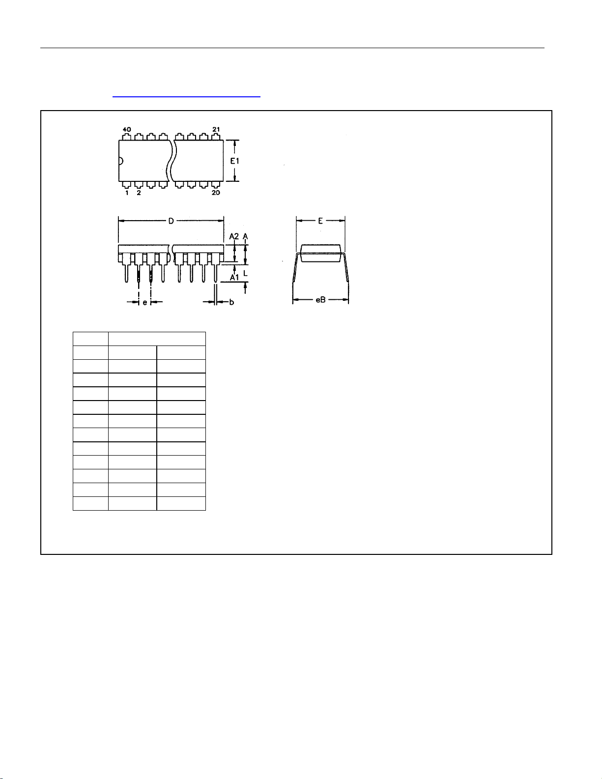
DS89C430/DS89C440/DS89C450 Ultra-High-Speed Flash Microcontrollers
PACKAGE INFORMATION
(The package drawing(s) in this data sheet may not reflect the most current specifications. For the latest package outline
information, go to www.maxim-ic.com/DallasPackInfo.)
PKG 40-PIN PDIP
DIM MIN MAX
A —
A1 0.015
A2 0.140
B 0.014
C 0.008
D 1.980
E 0.600
E1 0.530
E 0.090
L 0.115
EB 0.600
.
56-G5000-000
Note: Dimensions are in inches.
0.200
—
0.160
0.022
0.012
2.085
0.625
0.555
0.110
0.145
0.700
46 of 48
Page 47
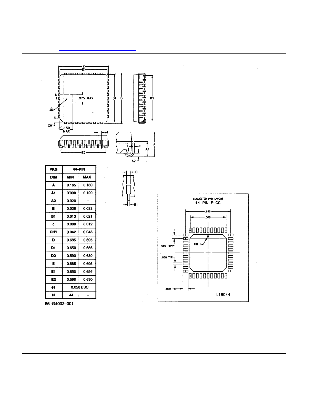
DS89C430/DS89C440/DS89C450 Ultra-High-Speed Flash Microcontrollers
PACKAGE INFORMATION (continued)
(The package drawing(s) in this data sheet may not reflect the most current specifications. For the latest package outline
information, go to www.maxim-ic.com/DallasPackInfo.)
NOTE 1: PIN 1 IDENTIFIER TO BE LOCATED IN ZONE INDICATED.
NOTE 2: CONTROLLING DIMENSION ARE IN INCHES.
47 of 48
Page 48

DS89C430/DS89C440/DS89C450 Ultra-High-Speed Flash Microcontrollers
PACKAGE INFORMATION (continued)
(The package drawing(s) in this data sheet may not reflect the most current specifications. For the latest package outline
information, go to www.maxim-ic.com/DallasPackInfo.)
Maxim/Dallas Semiconductor cannot assume responsibility for use of any circuitry other than circuitry entirely embodied in a Maxim/Dallas Semiconductor product.
No circuit patent licenses are implied. Maxim/Dallas Semiconductor reserves the right to change the circuitry and specifications without notice at any time.
Maxim Integrated Products, 120 San Gabriel Drive, Sunnyvale, CA 94086 408-737-7600
© 2003 Maxim Integrated Products · Printed USA
48 of 48
 Loading...