

Page 1
General Description
The DS4560 is a self-contained hot-plug switch intended to be used on +12V power buses to limit through
current and to control the power-up output-voltage
ramp. The device contains an on-board 25mΩ n-channel power MOSFET that is actively closed-loop controlled to ensure that an adjustable current limit is not
exceeded. The maximum allowable current through the
device is determined by an external resistor connected
to the ILIM pin.
The DS4560 also contains the ability to control the
power-up output-voltage ramp. A capacitor connected
to the VRAMP pin sets the desired voltage ramp rate.
The output voltage is unconditionally clamped to keep
input overvoltage stresses from harming the load. The
DS4560 also contains an adjustable power-up timer. A
capacitor connected to the TIMER pin determines how
long after power-on reset the DS4560 should wait
before starting to apply power to the load. The TIMER
pin can also be driven with a digital logic output to create a device-enable function.
The DS4560 contains an on-board temperature sensor
with hysteresis. If operating conditions cause the
device to exceed an internal thermal limit, the DS4560
either unconditionally shuts down and latches off awaiting a power-on reset (DS4560S-LO), or it waits until the
device has cooled by the hysteresis amount and then
restarts (DS4560S-AR).
Applications
Features
♦ On-Board 25mΩ Power MOSFET
♦ Adjustable Short-Circuit Current and Overload
Current Limit
♦ Adjustable Output-Voltage Slew Rate
♦ Adjustable Power-Up Timer with External Enable
Capability
♦ Output Overvoltage Limiting
♦ On-Board Thermal Protection
♦ On-Board Charge Pump
♦ Latchoff and Autoretry Versions Available
♦ 9.0V to 13.2V Supply Operation
♦ 8-Pin SO (150 mils) Pb-Free Package
DS4560
12V Hot-Plug Switch
________________________________________________________________
Maxim Integrated Products
1
Pin Configuration
Ordering Information
Rev 1; 9/08
For pricing, delivery, and ordering information, please contact Maxim Direct at 1-888-629-4642,
or visit Maxim’s website at www.maxim-ic.com.
+
Denotes a lead-free/RoHS-compliant package.
T = Tape and reel.
PART
THER MAL
SHUTDOWN
PIN-PACKAGE
DS4560S-LO+ Latchoff 8 SO
DS4560S-LO+T Latchoff 8 SO
DS4560S-AR+ Autoretry 8 SO
DS4560S-AR+T Autoretry 8 SO
Pin Description
PIN NAME FUNCTION
1 GND
Ground. This is a lso a heat sink for the
device.
2 VRAMP Output-Voltage Ramp Adjustment
3 TIMER Power-Up Timer/Enable
4 ILIM Current-Limit Adju stment
5, 6, 7 LOAD Output Load Connection (MOSFET Source)
8 VCC Input Supply Voltage (MOSFET Drain)
PCI Express is a registered trademark of PCI-SIG Corp.
InfiniBand is a trademark and service mark of the InfiniBand Trade Association.
RAID/Hard Drives
Servers/Routers
PCI/PCI Express
®
InfiniBand
SM
Base Stations
TOP VIEW
+
18V
GND
2 7 LOADVRAMP
DS4560
TIMER 3 6
45
SO (150 mils)
CC
LOAD
LOADILIM
Page 2
DS4560
12V Hot-Plug Switch
2 _______________________________________________________________________________________
ABSOLUTE MAXIMUM RATINGS
RECOMMENDED OPERATING CONDITIONS
(TJ= -40°C to +135°C.)
Stresses beyond those listed under “Absolute Maximum Ratings” may cause permanent damage to the device. These are stress ratings only, and functional
operation of the device at these or any other conditions beyond those indicated in the operational sections of the specifications is not implied. Exposure to
absolute maximum rating conditions for extended periods may affect device reliability.
Voltage Range on VCCand LOAD Relative to GND
Continuous .........................................................-0.3V to +18V
1ms Maximum ....................................................-0.3V to +22V
Voltage Range on ILIM and VRAMP
Relative to GND.....................................-0.3V to (V
CC
+ 0.3V),
but not to exceed +18V
Voltage Range on TIMER Relative to GND ...........-0.3V to +5.0V
Drain Current
Continuous ...........................................................................4A
Peak ...................................................................................15A
Operating Junction Temperature Range...........-40°C to +135°C
Storage Temperature Range .............................-55°C to +135°C
Soldering Temperature...........................Refer to the IPC/JEDEC
J-STD-020 Specification.
ELECTRICAL CHARACTERISTICS
(VCC= +12V, TJ= +25°C, unless otherwise noted.)
PARAMETER SYMBOL CONDITIONS MIN TYP MAX UNITS
Supply Voltage VCC (Notes 1, 2) 9.0 13.2 V
R
Value R
ILIM
C
C
TIMER Turn-On Voltage VON 2.6 5 V
TIMER Turn-Off Voltage V
Value C
VRAMP
Value C
TIMER
20 400
ILIM
0.04 5.00 μF
VRAMP
0.04 5.00 μF
TIMER
-0.3 +2.0 V
OFF
PARAMETER SYMBOL CONDITIONS MIN TYP MAX UNITS
Supply Current ICC (Note 3) 1.1 2.00 mA
UVLO Ri sing V
UVLO Falling V
UVLO Hysteresis V
On-Resistance RON 25 32 m
MOSFET Output Capacitance C
LOAD Voltage During Off State V
Dela y Time from Enable to
Beginning of Conduction
Gate-Charging Time from
Conduction to 90% of V
Shutdown Junction Temperature T
Thermal Hysteresis T
TIMER Charging Current I
Overvoltage Clamp V
OUT
7.5 8.0 8.5 V
UVLOR
6.5 7.0 7.5 V
UVLOF
1 V
UVLOH
500 pF
OUT
(Note 4) 200 mV
LOFF
t
C
POND
t
C
GCT
(Note 5) 120 135 150 °C
SHDN
(Note 5) 40 °C
HYS
70 80 92 μA
TIMER
13.5 15.0 16.5 V
OVC
= 1μF 5 ms
VRAMP
VRAMP
= 1μF, C
= 1000μF 48 66 80 ms
LOAD
Page 3
DS4560
12V Hot-Plug Switch
_______________________________________________________________________________________ 3
Note 1: All voltages are referenced to ground. Currents entering the IC are specified positive and currents exiting the IC are negative.
Note 2: This supply range guarantees that the LOAD voltage is not clamped by the overvoltage limit.
Note 3: Supply current specified with no load on the LOAD pin.
Note 4: V
LOFF
voltage specified with a 2.5mA load applied to LOAD.
Note 5: Not production tested. Guaranteed by design.
Note 6: I
SCL
is the current limit when the output voltage is initially ramping up.
Note 7: I
OVL
is the current limit after the output voltage ramping is complete.
ELECTRICAL CHARACTERISTICS (continued)
(VCC= +12V, TJ= +25°C, unless otherwise noted.)
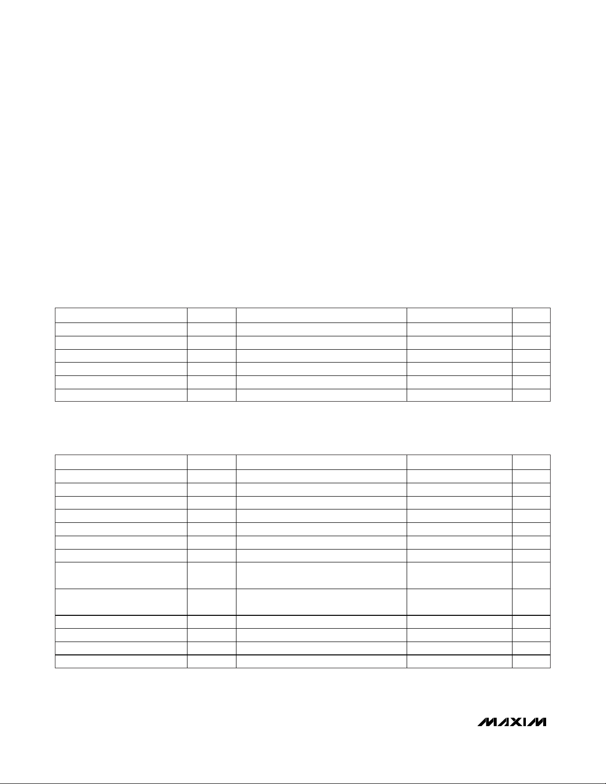
Typical Operating Characteristics
(V
CC
= 12V, TA = +25°C, R
ILIM
= 56Ω, VCC= 12V, C
TIMER
= 0.1µF, C
VRAMP
= 0.1µF, unless otherwise noted.)
Short-Circuit Limit I
Overload Limit I
LOAD Voltage Slew Rate SR
VRAMP Charging Current I
PARAMETER SYMBOL CONDITIONS MIN TYP MAX UNITS
R
SCL
R
OVL
C
LOAD
70 80 92 μA
VRAMP
= 56 (Note 6) 2.0 2.5 3.0 A
ILIM
= 56 (Note 7) 3.5 4.4 5.9 A
ILIM
= 1μF 0.13 0.15 0.18 V/ms
VRAMP
CURRENT LIMIT vs. R
10
1
CURRENT LIMIT (A)
ILIM
I
OVL
I
SCL
DS4560 toc01
CURRENT LIMIT (A)
CURRENT LIMIT vs. TEMPERATURE
7
6
5
4
3
2
1
I
OVL
I
SCL
OVERVOLTAGE CLAMP vs. TEMPERATURE
16.4
16.2
DS4560 toc02
16.0
15.8
15.6
15.4
OVERVOLTAGE CLAMP (V)
15.2
NO LOAD
10Ω LOAD
DS4560 toc03
0.1
100
R
(Ω)
ILIM
ON-RESISTANCE vs. TEMPERATURE
45
40
35
(mΩ)
ON
R
30
25
20
-40 140
TEMPERATURE (°C)
0
100010
-40 140
TEMPERATURE (°C)
12010080604020-20 0
15.0
-40 140
TEMPERATURE (°C)
12010080604020-20 0
TYPICAL DS4560 TURN-ON WAVEFORMS
SUPPLY CURRENT vs. TEMPERATURE
2.00
1.75
DS4560 toc04
1.50
1.25
(mA)
1.00
CC
I
0.75
0.50
0.25
0
120100806040200-20
-40 140
TEMPERATURE (°C)
DS4560 toc05
5V/div
0V
120100-20 0 20 6040 80
= 18V, 10Ω RESISTIVE LOAD
V
CC
V
CC
TIMER
LOAD
2ms/div
DS4560 toc06
VRAMP
Page 4

DS4560
12V Hot-Plug Switch
4 _______________________________________________________________________________________
Typical Operating Characteristics (continued)
(V
CC
= 12V, TA = +25°C, R
ILIM
= 56Ω, VCC= 12V, C
TIMER
= 0.1µF, C
VRAMP
= 0.1µF, unless otherwise noted.)
TURN-ON WAVEFORMS
10Ω RESISTIVE LOAD
DS4560 toc07
V
CC
LOAD
LOAD CURRENT
2V/div
0V
0mA
500mA/div
5ms/div
TURN-ON WAVEFORMS
3300μF CAPACITIVE LOAD
DS4560 toc08
V
CC
LOAD
LOAD CURRENT
2V/div
0V
0mA
500mA/div
5ms/div
TURN-ON WAVEFORMS
V
CC
= 18V, 10Ω RESISTIVE LOAD
DS4560 toc09
V
CC
LOAD
LOAD CURRENT
5V/div
0V
0mA
500mA/div
5ms
THERMAL SHUTDOWN WITH AUTORETRY
DS4560S-AR+, V
CC
= 18V, 10Ω RESISTIVE LOAD
DS4560 toc10
V
CC
LOAD
LOAD CURRENT
5V/div
0V
500mA/div
0mA
500ms/div
Page 5

DS4560
THERMAL
LIMIT
EXTERNAL DISABLE
TIMER
C
TIMER
+5V
2.5V
UVLO
CURRENT
LIMIT
CHARGE
PUMP
LOAD
+5V
VREG
OVERVOLTAGE
LIMIT
GND
R
R
R
ILIM
LOAD
ILIM
+12V
V
CC
VRAMP
V
CC
80μA
80μA
C
VRAMP
Block Diagram/Typical Application Circuit
DS4560
12V Hot-Plug Switch
_______________________________________________________________________________________ 5
Detailed Description
The DS4560 begins to operate when VCCexceeds the
undervoltage lockout level, V
UVLOR
. At this level, the
enable circuit and TIMER pin become active. Once the
device has been enabled, a gate voltage is applied to
the power MOSFET, allowing current to begin flowing
from VCCto LOAD. The speed of the output-voltage
ramp is controlled by the capacitance placed at the
VRAMP pin. The load current is continuously monitored
during the initial voltage ramping (I
SCL
) and during nor-
mal operation (I
OVL
). If the current exceeds the current
limit that is set by the external resistance at ILIM, the
gate voltage of the power MOSFET is decreased,
reducing the output current to the set current limit.
Current is limited by the DS4560 comparing the voltage
difference between the LOAD and ILIM pins to an internal reference voltage. If the output current exceeds the
limit that is set by the R
ILIM
resistor, the gate voltage of
the power MOSFET is decreased, which reduces the
output current to the load.
When the output power is initially ramping up, the current
limit is I
SCL
. Once the voltage ramping is complete, the
current limit is I
OVL
. The lower I
SCL
current limit protects
the source if there is a dead short on initial power-up.
The DS4560 acts as a fuse and automatically disables
the current flowing to the load when the temperature of
the power MOSFET has exceeded the shutdown junction temperature, T
SHDN
.
Page 6

DS4560
12V Hot-Plug Switch
6 _______________________________________________________________________________________
Enable/Timer
The voltage level of the TIMER pin is compared to an
internal source (see the
Block Diagram)
. When the level
on the pin exceeds VON, the comparator outputs a low
level. This then turns on the voltage ramp circuit,
enabling the device’s output. This TIMER pin can be
configured into one of four different modes of operation
listed in Table 1. The TIMER pin was designed to work
with most logic families. The TIMER pin will have at
least 250mV of hysteresis between V
ON
and V
OFF
. It is
recommended that any logic gate used to drive the
TIMER pin be tested to ensure proper operation.
Once the device has been enabled, there is a delay
(t
POND
) until conduction begins from VCCto LOAD.
This delay is the time required for the charge pump to
bring the gate voltage of the power MOSFET above its
threshold level. Once the gate is above the threshold
level, conduction begins and the output voltage begins
ramping.
Automatic Enable Mode
When VCCexceeds V
UVLOR
, the gate holding the
TIMER node low is released. The internal current
source brings the node to a level greater than VON,
enabling the device.
Delayed Automatic Enable Mode
When VCCexceeds V
UVLOR
, the gate holding the
TIMER node low is released. The internal current
source (I
TIMER
) then begins charging C
TIMER
. When
C
TIMER
is charged to a level greater than VON, the
device turns on. The equation for the delay time is:
t
DELAY
= (C
TIMER
x VON)/I
TIMER
Enable/Disable Mode
A logic gate or open-collector device can be connected to the TIMER pin to enable or disable the device.
When the TIMER pin is held low, the device is disabled.
When an open-collector device is used to drive the
TIMER pin, the DS4560 is enabled when the open collector is in its high-impedance state by the internal current source bringing the TIMER node high. The TIMER
pin is also compatible with most logic families if the out-
put high voltage level of the gate exceeds the V
ON
level, and the gate can sink the I
TIMER
current.
Enable with Delay/Disable Mode
An open-collector device is connected in parallel with
C
TIMER
. When the pin is held low, the DS4560 is disabled. When the open-collector driver is high impedance, the internal current source begins to charge
C
TIMER
as in the delayed mode.
Output-Voltage Ramp
The voltage ramp circuit uses an operational amplifier
to control the gate bias of the n-channel power
MOSFET. When the timer/enable circuit is disabled, a
FET is used to keep C
VRAMP
discharged, which forces
the output voltage to GND. Once the enable/timer circuit has been enabled, an internal current source,
I
VRAMP
, begins to charge the external capacitor,
C
VRAMP
, connected to the VRAMP pin. The amplifier
controls the gate of the power MOSFET so that the
LOAD output voltage divided by two tracks the rising
voltage level of C
VRAMP
. The output voltage continues
to ramp until it reaches either the input V
CC
level or the
overvoltage clamp limits. The equation for the outputvoltage ramp function is:
dV
LOAD
/dt = 2 x (I
VRAMP/CVRAMP
)
Thermal Shutdown
The DS4560 enters a thermal shutdown state when the
temperature of the power MOSFET reaches or exceeds
T
SHDN
, approximately +135°C. When T
SHDN
is exceeded, the thermal-limiting circuitry disables the DS4560
using the enable circuitry. The DS4560 is offered in two
different versions: an autoretry version and a latchoff
version.
Autoretry Version (DS4560S-AR)
The autoretry verson continually monitors the temperature once it has entered thermal shutdown. If the junction temperature falls below approximately +95°C
(T
SHDN
- T
HYS
), the power MOSFET is re-enabled. See
the THERMAL SHUTDOWN WITH AUTORETRY graph
for details.
Table 1. TIMER Pin Modes
MODE OF OPERATION TIMER PIN SETUP
Automatic Enable No connection to TIMER pin.
Delayed Automatic Enable Capacitor C
Enable/Disable Open-collector device.
Enable with Delay/Disable Open-collector device and C
connected to TIMER.
TIMER
TIMER
.
Page 7

DS4560
12V Hot-Plug Switch
_______________________________________________________________________________________ 7
Latchoff Version (DS4560S-LO)
Once the latchoff version has entered thermal shutdown, it does not attempt to turn back on. The only way
to turn this device back on is to cycle the power to the
device. When power is reapplied to V
CC
, the junction
temperature needs to be less than T
SHDN
for the
device to be enabled.
Overvoltage Limit
The overvoltage-limiting clamp monitors the VRAMP
level compared to an internal voltage reference. When
the voltage on VRAMP exceeds V
OVC
/2, the gate voltage of the n-channel power MOSFET is reduced, limiting the voltage on LOAD to V
OVC
even as V
CC
increases. If the device is in overvoltage for an extended period of time, the device may overheat and enter
thermal shutdown. This is caused by the power created
by the voltage drop across the power MOSFET and the
load current. See the THERMAL SHUTDOWN WITH
AUTORETRY graph for details.
Applications Information
The GND pin of the DS4560 is also a heat sink for the
device. This pin should be connected to a large trace
or plane capable of dissipating heat from the device.
PACKAGE TYPE PACKAGE CODE DOCUMENT NO.
8 SO —
21-0041
Package Information
For the latest package outline information and land patterns, go
to www.maxim-ic.com/packages
.
Page 8

DS4560
12V Hot-Plug Switch
Maxim cannot assume responsibility for use of any circuitry other than circuitry entirely embodied in a Maxim product. No circuit patent licenses are
implied. Maxim reserves the right to change the circuitry and specifications without notice at any time.
8
_____________________Maxim Integrated Products, 120 San Gabriel Drive, Sunnyvale, CA 94086 408-737-7600
© 2008 Maxim Integrated Products is a registered trademark of Maxim Integrated Products, Inc.
Revision History
REVISION
NUMBER
0 6/08 Initial release. —
1 9/08
REVISION
DATE
In the Recommended Operating Conditions, changed the TIMER Turn-On Voltage
) maximum specification from “VCC + 0.3V” to “5V.”
(V
ON
DESCRIPTION
PAGES
CHANGED
2
 Loading...