

Page 1
DS4432
Dual-Channel, I2C, 7-Bit Sink/Source
Current DAC
________________________________________________________________
Maxim Integrated Products
1
Rev 0; 12/08
For pricing, delivery, and ordering information, please contact Maxim Direct at 1-888-629-4642,
or visit Maxim’s website at www.maxim-ic.com.
General Description
The DS4432 contains two I2C programmable current
DACs that are each capable of sinking and sourcing
current up to 200µA. Each DAC output has 127 sink
and 127 source settings that are programmed using the
I2C interface. The current DAC outputs power up in a
high-impedance state.
Applications
Power-Supply Adjustment
Power-Supply Margining
Adjustable Current Sink or Source
Features
♦ Two Current DACs
♦ Full-Scale Current 50µA to 200µA
♦ Full-Scale Range for Each DAC Determined by
External Resistors
♦ 127 Settings Each for Sink and Source Modes
♦ I
2
C-Compatible Serial Interface
♦ Low Cost
♦ Small Package (8-Pin µSOP)
♦ -40°C to +85°C Temperature Range
♦ 2.7V to 5.5V Operating Range
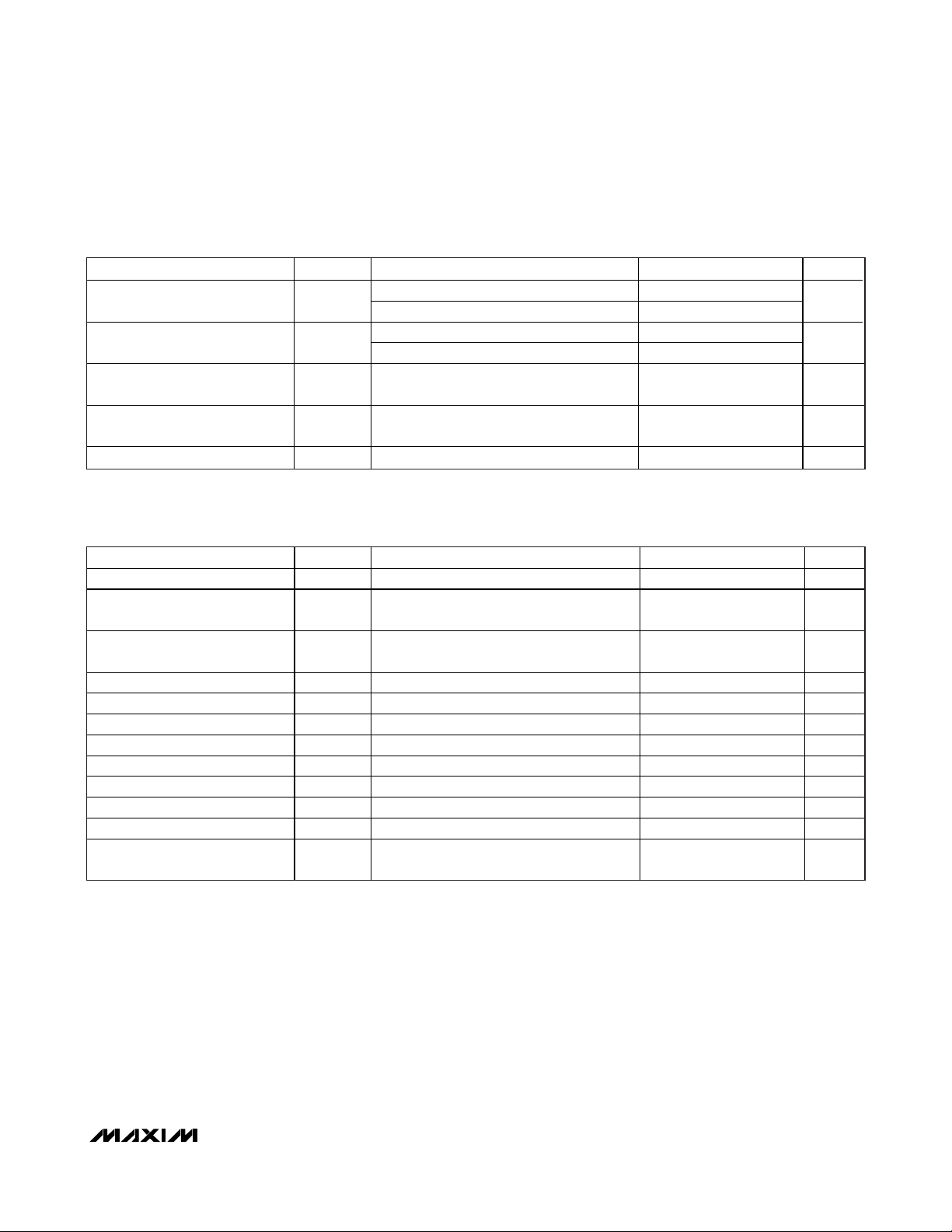
DC-DC
CONVERTER
FB
OUT
SDA
SCL
OUT0
OUT1
GND
R
FS0
R
FS1
4.7kΩ4.7kΩ
V
CC
V
CC
V
OUT0
FS0
FS1
R
0B
R
0A
DC-DC
CONVERTER
FB
OUT
V
OUT1
R
1B
R
1A
DS4432
Typical Operating Circuit
Ordering Information
+
Denotes a lead(Pb)-free/RoHS-compliant package.
T&R = Tape and reel.
μ
Pin Configuration
TOP VIEW
+
18V
SDA
2 7 OUT1SCL
DS4432
CC
OUT0FS1 3 6
FS0GND 4 5
PART TEMP RANGE PIN-PACKAGE
DS4432U+ -40°C to +85°C 8 μSOP
DS4432U+T&R -40°C to +85°C 8 μSOP
SOP
Page 2
DS4432
Dual-Channel, I2C, 7-Bit Sink/Source
Current DAC
2 _______________________________________________________________________________________
ABSOLUTE MAXIMUM RATINGS
RECOMMENDED OPERATING CONDITIONS
(TA= -40°C to +85°C.)
Stresses beyond those listed under “Absolute Maximum Ratings” may cause permanent damage to the device. These are stress ratings only, and functional
operation of the device at these or any other conditions beyond those indicated in the operational sections of the specifications is not implied. Exposure to
absolute maximum rating conditions for extended periods may affect device reliability.
Voltage Range on VCC, SDA, and SCL
Relative to Ground.............................................-0.5V to +6.0V
Voltage Range on FS0, FS1, OUT0, OUT1
Relative to Ground..................................-0.5V to (V
CC
+ 0.5V)
(Not to exceed 6.0V.)
Operating Temperature Range ...........................-40°C to +85°C
Storage Temperature Range .............................-55°C to +125°C
Soldering Temperature ...............................Refer to the IPC/JEDEC
J-STD-020 Specification.
DC ELECTRICAL CHARACTERISTICS
(VCC= +2.7V to +5.5V, TA= -40°C to +85°C.)
OUTPUT CURRENT SOURCE CHARACTERISTICS
(VCC= +2.7V to +5.5V, TA= -40°C to +85°C.)
Supply Voltage VCC (Note 1) 2.7 5.5 V
Input Logic 1 (SDA, SCL) VIH 0.7 x VCC VCC + 0.3 V
Input Logic 0 (SDA, SCL) VIL -0.3 0.3 x VCC V
Ful l-Scale Re sistor Values R
PARAMETER S YMBOL CONDITIONS MIN TYP MAX UNITS
, R
FS0
(Note 2) 40 160 k
FS1
Supply Current ICC VCC = 5.5V (Note 3) 150 μA
Input Leakage (SDA, SCL) IIL VCC = 5.5V 1 μA
Output Leakage (SDA) IL 1 μA
Output Current Low (SDA) I
RFS Voltage V
I/O Capacitance C
PARAMETER S YMBOL CONDITIONS MIN TYP MAX UNITS
OL
RFS
I/O
VOL = 0.4V 3
VOL = 0.6V 6
0.997 V
10 pF
mA
Output Voltage for Sinking Current V
Output Voltage for Sourcing
Current
Ful l-Scale Sink Output Current I
Ful l-Scale Source Output Current I
Output Current Ful l-Scale
Accuracy
Output Current Temperature
Coefficient
PARAMETER S YMBOL CONDITIONS MIN TYP MAX UNITS
OUT:SINK
V
OUT: SOU RCE
OUT:SINK
OUT: SOURC E
I
OUT:FS
I
OUT:TC
(Note 4) 0.5 3.5 V
(Note 4) 0
(Notes 1, 4) 50 200 μA
(Notes 1, 4) -200 -50 μA
+25°C, VCC = 3.3V; using 0.1% R
resistor, V
(Note 5) ±130 ppm/°C
OUT0
= V
= 1.2V (Note 2)
OUT1
FS
±5 %
V
CC
0.75
V
Page 3
DS4432
Dual-Channel, I2C, 7-Bit Sink/Source
Current DAC
_______________________________________________________________________________________ 3
Note 1: All voltages with respect to ground. Currents entering the IC are specified positive, and currents exiting the IC are negative.
Note 2: Input resistors (R
FS
) must be between the specified values to ensure the device meets its accuracy and linearity specifications.
Note 3: Supply current specified with all outputs set to zero current setting. SDA and SCL are connected to V
CC
. Excludes current
through R
FS
resistors (I
RFS
). Total current including I
RFS
is ICC+ (2 x I
RFS
).
Note 4: The output voltage range must be satisfied to ensure the device meets its accuracy and linearity specifications.
Note 5: Temperature drift excludes drift caused by external resistor.
Note 6: Differential linearity is defined as the difference between the expected incremental current increase with respect to position
and the actual increase. The expected incremental increase is the full-scale range divided by 127.
Note 7: Guaranteed by design.
Note 8: Integral linearity is defined as the difference between the expected value as a function of the setting and the actual value.
The expected value is a straight line between the zero and the full-scale values proportional to the setting.
Note 9: Timing shown is for fast-mode (400kHz) operation. This device is also backward compatible with I
2
C standard-mode timing.
Note 10: C
B
—total capacitance of one bus line in pF.
OUTPUT CURRENT SOURCE CHARACTERISTICS (continued)
(VCC= +2.7V to +5.5V, TA= -40°C to +85°C.)
AC ELECTRICAL CHARACTERISTICS
(VCC= +2.7V to +5.5V, TA= -40°C to +85°C.)
PARAMETER S YMBOL CONDITIONS MIN TYP MAX UNITS
Output Current Variation Due to
Power-Supply Change
Output Current Variation Due to
Output-Voltage Change
Output Leakage Current at Zero
Current Setting
Output Current Differential
Linearity
Output Current Integral Linearity INL (Notes 7, 8) -1 +1 LSB
I
ZERO
DNL (Notes 6, 7) -0.5 +0.5 LSB
DC source, V
DC sin k, V
DC source, VCC = 3.3V 0.08
DC sin k, V
-1 +1 μA
measured at 1.2V 0.41
OUT
measured at 1.2V 0.41
OUT
= 3.3V 0.14
CC
%/V
%/V
SCL Clock Frequenc y f
Bus Free Time Between STOP
and START Conditions
Hold Time (Repeated) START
Condition
Low Period of SCL t
High Period of SCL t
Data Hold Time t
Data Setup Time t
START Setup Time t
SDA a nd SCL R i se Time tR (Note 10) 20 + 0.1CB 300 ns
SDA and SCL Fall Time tF (Note 10) 20 + 0.1CB 300 ns
STOP Setup Time t
SDA a nd SCL Capacit i ve
Loading
PARAMETER S YMBOL CONDITIONS MIN TYP MAX UNITS
(Note 9) 0 400 kHz
SCL
t
1.3 μs
BUF
t
0.6 μs
HD: STA
1.3 μs
LOW
0.6 μs
HIGH
0 0.9 μs
HD:DAT
100 ns
SU:DAT
0.6 μs
SU:STA
0.6 μs
SU:STO
(Note 10) 400 pF
C
B
Page 4

DS4432
Dual-Channel, I2C, 7-Bit Sink/Source
Current DAC
4 _______________________________________________________________________________________
Pin Description
Typical Operating Characteristics
(Applies to OUT0 and OUT1. VCC= 2.7V to 5.0V, SDA = SCL = VCC, TA= +25°C, and no loads on OUT0, OUT1, FS0, or FS1, unless
otherwise noted.)
SUPPLY CURRENT
vs. SUPPLY VOLTAGE
DS4432 toc01
SUPPLY VOLTAGE (V)
SUPPLY CURRENT (μA)
5.04.54.03.53.0
25
50
75
100
125
150
0
2.5 5.5
DOES NOT INCLUDE CURRENT DRAWN BY
RESISTORS CONNECTED TO FS0 OR FS1.
SUPPLY CURRENT
vs. TEMPERATURE
DS4432 toc02
TEMPERATURE (°C)
SUPPLY CURRENT (μA)
60 8040200-20
25
50
75
100
125
150
0
-40
DOES NOT INCLUDE CURRENT DRAWN BY
RESISTORS CONNECTED TO FS0 OR FS1.
VCC = 5.5V
VCC = 3.3V
VCC = 2.7V
VOLTCO (SOURCE)
DS4432 toc03
V
OUT
(V)
I
OUT
(μA)
4321
-225
-200
-175
-150
-250
05
40kΩ LOAD ON FS0 AND FS1.
VOLTCO (SINK)
DS4432 toc04
V
OUT
(V)
I
OUT
(μA)
3.53.02.52.01.51.00.5
175
200
225
250
150
0 4.0
40kΩ LOAD ON FS0 AND FS1.
TEMPERATURE COEFFICIENT
vs. SETTING (SOURCE)
DS4432 toc05
SETTING (DEC)
TEMPERATURE COEFFICIENT (°C/ppm)
100 125755025
0
50
100
150
200
250
300
-50
0
RANGE FOR THE 50μA TO 200μA CURRENT
SOURCE RANGE.
+25°C TO -40°C
+25°C TO +85°C
TEMPERATURE COEFFICIENT
vs. SETTING (SINK)
DS4432 toc06
SETTING (DEC)
TEMPERATURE COEFFICIENT (°C/ppm)
100 125755025
-150
-50
50
150
250
350
450
550
650
-250
0
RANGE FOR THE 50μA TO 200μA CURRENT
SINK RANGE.
+25°C TO -40°C
+25°C TO +85°C
NAME PIN FUNCTION
SDA 1 I2C Serial Data. Input/output for I2C data.
SCL 2 I2C Serial Clock. Input for I2C clock.
FS1 3
FS0 5
GND 4 Ground
OUT0 6
OUT1 7
VCC 8 Power Supply
Ful l-Scale Calibration Inputs. A resistor to ground on the se pins determines the full-scale current
for each output. FS0 controls OUT0; FS1 controls OUT1.
Current Outputs. Sinks or source s the current determined by the register setting s and the
resistance connected to FS0 and FS1.
Page 5

DS4432
Dual-Channel, I2C, 7-Bit Sink/Source
Current DAC
_______________________________________________________________________________________ 5
Block Diagram
Typical Operating Characteristics (continued)
(Applies to OUT0 and OUT1. VCC= 2.7V to 5.0V, SDA = SCL = VCC, TA= +25°C, and no loads on OUT0, OUT1, FS0, or FS1, unless
otherwise noted.)
INTEGRAL LINEARITY
DS4432 toc07
SETTING (DEC)
INL (LSB)
100 125755025
-0.8
-0.6
-0.4
-0.2
0
0.2
0.4
0.6
0.8
1.0
-1.0
0
RANGE FOR THE 50μA TO 200μA CURRENT
SOURCE AND SINK RANGE.
DIFFERENTIAL LINEARITY
DS4432 toc08
SETTING (DEC)
DNL (LSB)
100 125755025
-0.8
-0.6
-0.4
-0.2
0
0.2
0.4
0.6
0.8
1.0
-1.0
0
RANGE FOR THE 50μA TO 200μA CURRENT
SOURCE AND SINK RANGE.
SDA SCL
V
V
CC
GND
CC
SOURCE OR
SINK MODE
F8h F9h
CURRENT
DAC0
FS0
R
FS0
I2C-COMPATIBLE
SERIAL INTERFACE
127 POSITIONS
EACH FOR SINK
AND SOURCE
MODE
FS1
R
CURRENT
FS1
DS4432
DAC1
OUT1OUT0
Page 6

DS4432
Dual-Channel, I2C, 7-Bit Sink/Source
Current DAC
6 _______________________________________________________________________________________
Detailed Description
The DS4432 contains two I2C adjustable current DACs
that are each capable of sinking and sourcing current.
Each output (OUT0 and OUT1) has 127 sink and 127
source settings that can be controlled by the I2C interface. The full-scale ranges and corresponding step
sizes of the outputs are determined by external resistors, connected to pins FS0 and FS1.
The formula to determine RFS(connected to the FSx
pins) to attain the desired full-scale current range is:
Equation 1:
where I
FS
is the desired full-scale current value, V
RFS
is
the RFSvoltage (see the
DC Electrical Characteristics
table), and RFSis the external resistor value.
To calculate the output current value (I
OUT
) based on the
corresponding DAC value (see Table 1 for corresponding
memory addresses), use equation 2.
Equation 2:
On power-up the DS4432 outputs zero current. This is
done to prevent the device from sinking or sourcing an
incorrect amount of current before the system host controller has had a chance to modify the DS4432’s setting.
As a source for biasing instrumentation or other circuits,
the DS4432 provides a simple and inexpensive current
DAC with an I
2
C interface for control. The adjustable
full-scale range allows the application to get the most
out of its 7-bit sink or source resolution.
When used in adjustable power-supply applications
(see the
Typical Operating Circuit
), the DS4432 does
not affect the initial power-up voltage of the supply
because it defaults to providing zero output current on
power-up. As the device sources or sinks current into
the feedback-voltage node, it changes the amount of
output voltage required by the regulator to reach its
steady-state operating point. Using the external resistor,
R
FS
, to set the output current range, the DS4432 provides some flexibility for adjusting the impedances of
the feedback network or the range over which the power
supply can be controlled or margined.
Memory Organization
To control the DS4432’s current sources, write to the
memory addresses listed in Table 1.
The format of each output control register is:
where:
Example: R
FS0
= 80kΩ and register 0xF8h is written to
a value of 0xAAh. Calculate the output current.
IFS= (0.997V/80kΩ) x (127/16) = 98.921µA
The MSB of the output register is 1, so the output is sourcing the value corresponding to position 2Ah (42 decimal).
The magnitude of the output current is equal to:
98.921µA x (42/127) = 32.714µA
I
2
C Serial Interface Description
I2C Slave Address
The DS4432’s slave address is 90h.
I2C Definitions
The following terminology is commonly used to describe
I2C data transfers:
Master Device: The master device controls the slave
devices on the bus. The master device generates
SCL clock pulses and START and STOP conditions.
Table 1. Memory Addresses
R
I
OUT FS
V
RFS
FS
=
16 I
× 127
×
FS
D
AC Value dec()
=×
1
27
I
MEMORY ADDRESS
(HEX)
F8h OUT0
F9h OUT1
MSB LSB
S D
D5 D4 D3 D2 D1 D
6
BIT NAME FUNCTION
Determines if DAC sources or
Sign
S
DX Data
sinks current. For sink
Bit
S = 0; for source S = 1.
7-Bit Data Control ling DAC
Output. Setting 0000000b
outputs zero current regardle ss
of the state of the sign bit.
CURRENT SOURCE
0
POWER-ON
DEFAULT
0b
0000000b
Page 7

DS4432
Dual-Channel, I2C, 7-Bit Sink/Source
Current DAC
_______________________________________________________________________________________ 7
Slave Devices: Slave devices send and receive
data at the master’s request.
Bus Idle or Not Busy: Time between STOP and
START conditions when both SDA and SCL are inactive and in their logic-high states. When the bus is
idle it often initiates a low-power mode for slave
devices.
START Condition: A START condition is generated
by the master to initiate a new data transfer with a
slave. Transitioning SDA from high to low while SCL
remains high generates a START condition. See
Figure 1 for applicable timing.
STOP Condition: A STOP condition is generated by
the master to end a data transfer with a slave.
Transitioning SDA from low to high while SCL
remains high generates a STOP condition. See
Figure 1 for applicable timing.
Repeated START Condition: The master can use a
repeated START condition at the end of one data
transfer to indicate that it will immediately initiate a
new data transfer following the current one. Repeated
STARTs are commonly used during read operations
to identify a specific memory address to begin a data
transfer. A repeated START condition is issued identically to a normal START condition. See Figure 1 for
applicable timing.
Bit Write: Transitions of SDA must occur during the
low state of SCL. The data on SDA must remain valid
and unchanged during the entire high pulse of SCL,
plus the setup and hold time requirements (Figure 1).
Data is shifted into the device during the rising edge
of the SCL.
Bit Read: At the end of a write operation, the master
must release the SDA bus line for the proper amount
of setup time (Figure 1) before the next rising edge of
SCL during a bit read. The device shifts out each bit of
data on SDA at the falling edge of the previous SCL
pulse and the data bit is valid at the rising edge of the
current SCL pulse. Remember that the master generates all SCL clock pulses, including when it is reading
bits from the slave.
Acknowledgement (ACK and NACK): An
Acknowledgement (ACK) or Not Acknowledge
(NACK) is always the ninth bit transmitted during a
byte transfer. The device receiving data (the master
during a read or the slave during a write operation)
performs an ACK by transmitting a zero during the
ninth bit. A device performs a NACK by transmitting
a one during the ninth bit. Timing for the ACK and
NACK is identical to all other bit writes (Figure 2). An
ACK is the acknowledgement that the device is
properly receiving data. A NACK is used to terminate a read sequence or as an indication that the
device is not receiving data.
Byte Write: A byte write consists of 8 bits of information transferred from the master to the slave (most significant bit first) plus a 1-bit acknowledgement from
the slave to the master. The 8 bits transmitted by the
master are done according to the bit-write definition,
and the acknowledgement is read using the bit-read
definition.
Figure 1. I2C Timing Diagram
SDA
t
BUF
t
LOW
SCL
t
HD:STA
STOP START REPEATED
NOTE: TIMING IS REFERENCED TO V
IL(MAX)
AND V
IH(MIN)
t
R
t
HD:DAT
.
t
HIGH
t
F
t
SU:DAT
START
t
SU:STA
t
HD:STA
t
SP
t
SU:STO
Page 8

DS4432
Dual-Channel, I2C, 7-Bit Sink/Source
Current DAC
8 _______________________________________________________________________________________
Byte Read: A byte read is an 8-bit information trans-
fer from the slave to the master plus a 1-bit ACK or
NACK from the master to the slave. The 8 bits of
information that are transferred (most significant bit
first) from the slave to the master are read by the
master using the bit-read definition, and the master
transmits an ACK using the bit-write definition to
receive additional data bytes. The master must
NACK the last byte read to terminate communication
so the slave returns control of SDA to the master.
Slave Address Byte: Each slave on the I2C bus
responds to a slave address byte sent immediately following a START condition. The slave address byte
contains the slave address in the most significant 7
bits, and the R/W bit in the least significant bit. The
DS4432’s slave address is 90h.
When the R/W bit is 0 (such as in 90h), the master is
indicating it will write data to the slave. If R/W = 1
(91h in this case), the master is indicating it wants to
read from the slave. If an incorrect slave address is
written, the DS4432 assumes the master is communicating with another I2C device and ignores the
communication until the next START condition is
sent.
Memory Address: During an I
2
C write operation,
the master must transmit a memory address to identify the memory location where the slave is to store
the data. The memory address is always the second
byte transmitted during a write operation following
the slave address byte.
I2C Communication
Writing to a Slave: The master must generate a START
condition, write the slave address byte (R/W = 0), write
the memory address, write the byte of data, and generate a STOP condition. Remember that the master must
read the slave’s acknowledgement during all byte-write
operations.
Reading from a Slave: To read from the slave, the
master generates a START condition, writes the slave
address byte with R/W = 1, reads the data byte with a
NACK to indicate the end of the transfer, and generates
a STOP condition.
Applications Information
Example Calculation
for an Adjustable Power Supply
In this example, the typical operating circuit is used to
create Figure 3, a 2.0V voltage supply with ±20% margin. The adjustable power supply has a DC-DC converter output voltage, V
OUT
, of 2.0V and a DC-DC converter
feedback voltage, VFB, of 0.8V. To determine the relationship of R0Aand R0B, start with the equation:
Substituting VFB= 0.8V and V
OUT
= 2.0V, the relation-
ship between R0Aand R0Bis determined to be:
R0A= 1.5 x R
0B
Figure 2. I2C Communication Examples
2
C WRITE TRANSACTION
TYPICAL I
MSB LSB MSB LSB MSB LSB
START
1 0 0 1 0 0 0 R/W
SLAVE
b7 b6 b5 b4 b3 b2 b1 b0
ACK
SLAVE
b7 b6 b5 b4 b3 b2 b1 b0
ACK
SLAVE
ACK
STOP
SLAVE
ADDRESS
READ/
WRITE
EXAMPLE I2C TRANSACTIONS
SINGLE BYTE WRITE
A)
-WRITE RESISTOR
F9h TO 00h
B)
SINGLE BYTE READ
-READ RESISTOR F8h
START
START
90h F9h
90h
SLAVE
ACK
SLAVE
ACK
1 0010000
1 0010000
11111 001
11111 000
REGISTER/MEMORY ADDRESS
SLAVE
ACK
F8h
SLAVE
ACK
DATA
00000 000
REPEATED
START
SLAVE
ACK
91h
10010 001
STOP
SLAVE
ACK
DATA
MASTER
NACK
STOP
V
R
0
=
FB
RR
00
AB
B
+
V
×
OUT
Page 9

DS4432
Dual-Channel, I2C, 7-Bit Sink/Source
Current DAC
Maxim cannot assume responsibility for use of any circuitry other than circuitry entirely embodied in a Maxim product. No circuit patent licenses are
implied. Maxim reserves the right to change the circuitry and specifications without notice at any time.
Maxim Integrated Products, 120 San Gabriel Drive, Sunnyvale, CA 94086 408-737-7600 _____________________
9
© 2008 Maxim Integrated Products is a registered trademark of Maxim Integrated Products, Inc.
I
OUT0
is chosen to be 100µA (midrange source/sink
current for the DS4432). Summing the currents into the
feedback node, we have the following:
where
and
To create a 20% margin in the supply voltage, the value
of V
OUT
is set to 2.4V. With these values in place, R
0B
is calculated to be 2.67kΩ, and R0Ais calculated to be
4kΩ. The current DAC in this configuration allows the
output voltage to be moved linearly from 1.6V to 2.4V
using 127 settings. This corresponds to a resolution of
6.3mV/step.
VCCDecoupling
To achieve the best results when using the DS4432,
decouple the power supply with a 0.01µF or 0.1µF
capacitor. Use a high-quality ceramic surface-mount
capacitor if possible. Surface-mount components minimize lead inductance, which improves performance,
and ceramic capacitors tend to have adequate highfrequency response for decoupling applications.
Figure 3. Example Application Circuit
PACKAGE TYPE PACKAGE CODE DOCUMENT NO.
8 µSOP U8+1
21-0036
Package Information
For the latest package outline information and land patterns, go to www.maxim-ic.com/packages.
III
= −
OUT R B R A00 0
V
FB
=
R
B00
−
VV
OUT FB
R
A00
4.7kΩ4.7kΩ
SDA
SCL
GND
DS4432
V
CC
OUT0
I
RA
I
RB
=
V
CC
DC-DC
CONVERTER
OUT
FB
V
= 2.0V*
OUT
I
R0A
I
R0B
R0A = 4kΩ
VFB = 0.8V*
R0B = 2.67kΩ
FS0
I
R
= 80kΩ
FS0
*V
AND VFB VALUES ARE DETERMINED BY THE DC-DC CONVERTER AND SHOULD NOT BE CONFUSED WITH V
OUT
OUT0
OUT
AND V
OF THE DS4432.
RFS
 Loading...