

Page 1
General Description
The DS4426 contains four I2C-adjustable current DACs
capable of sinking or sourcing current. External resistors set the full-scale range of each output. Each DAC
output has 127 sink and 127 source steps that are programmed by the I2C interface. Power-supply tracking
functionality is provided for three channels using dedicated control inputs. Once power-supply tracking is
accomplished, the current outputs default to zero. Two
address pins allow up to four DS4426 devices to exist
on the same I2C bus.
Applications
Power-Supply Adjustment
Power-Supply Margining
Power-Supply Tracking
Adjustable Current Sink or Source
Features
♦ Four Current DACs
50µA to 200µA Adjustable Full-Scale Range
127 Settings Each for Sink and Source
♦ Power-Supply Tracking
Power-Supply Sequencing
Ramp-Up and Ramp-Down Tracking Control
Ratiometric Tracking Support
♦ +2.7V to +5.5V Operation
♦ I
2
C-Compatible Serial Interface
♦ Two Address Input Pins Allow Up to Four Devices
on Same I
2
C Bus
♦ Lead-Free, 28-Pin TQFN Package (4mm x 4mm)
with Exposed Pad
♦ Industrial Temperature Range: -40°C to +85°C
DS4426
Quad-Channel, I2C-Margining IDACs with
Three Channels of Power-Supply Tracking
________________________________________________________________
Maxim Integrated Products
1
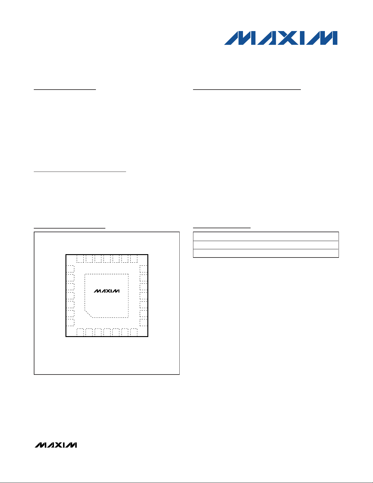
Pin Configuration
Ordering Information
19-4541; Rev 1; 7/09
For pricing, delivery, and ordering information, please contact Maxim Direct at 1-888-629-4642,
or visit Maxim’s website at www.maxim-ic.com.
+
Denotes a lead(Pb)-free/RoHS-compliant package.
T&R = Tape and reel.
*
EP = Exposed pad.
PART TEMP RANGE PIN-PACKAGE
DS4426T+ -40°C to +85°C 28 TQFN-EP*
DS4426T+T&R -40°C to +85°C 28 TQFN-EP*
Functional Diagram appears at end of data sheet.
TOP VIEW
THR1
DNC
THR3
THR2
18
DS4426
*EP
4567
CC
V
OUT0
OUT1
INN3
OUT2
INP3
OUT3
14
INN2
INP2
13
12
INN1
INP1
11
10
A1
A0
9
8
GND
FS1
22
FS2
23
24
FS3
25
GAIN3
26
GAIN2
27
GAIN1
28
N.C.
*EXPOSED PAD.
FS0
2021 19 17 16 15
+
12
3
SCL
SDA
THIN QFN
(4mm × 4mm)
Page 2
DS4426
Quad-Channel, I2C-Margining IDACs with
Three Channels of Power-Supply Tracking
2 _______________________________________________________________________________________
ABSOLUTE MAXIMUM RATINGS
RECOMMENDED OPERATING CONDITIONS
(TA= -40°C to +85°C.)
Stresses beyond those listed under “Absolute Maximum Ratings” may cause permanent damage to the device. These are stress ratings only, and functional
operation of the device at these or any other conditions beyond those indicated in the operational sections of the specifications is not implied. Exposure to
absolute maximum rating conditions for extended periods may affect device reliability.
Voltage Range on SDA, SCL Relative to GND ......-0.5V to +6.0V
Voltage Range on V
CC
Relative to GND ...............-0.5V to +6.0V
Voltage Range on A0, A1, FS[3:0], GAIN[3:1],
INN[3:1], INP[3:1], THR[3:1], and OUT[3:0]
Relative to GND ......................................-0.5V to (V
CC
+ 0.5V)*
Operating Temperature Range ...........................-40°C to +85°C
Storage Temperature Range .............................-55°C to +125°C
Soldering Temperature...........................Refer to the IPC/JEDEC
J-STD-020 Specification.
DC ELECTRICAL CHARACTERISTICS
(VCC= +2.7V to +5.5V, TA= -40°C to +85°C.)
DAC OUTPUT CURRENT CHARACTERISTICS
(VCC= +2.7V to +5.5V, TA= -40°C to +85°C.)
*
Not to exceed +6.0V.
PARAMETER SYMBOL CONDITIONS MIN TYP MAX UNITS
Supply Voltage VCC (Note 1) 2.7 5.5 V
Input Logic 1
(SDA, SCL, A0, A1)
Input Logic 0
(SDA, SCL, A0, A1)
Full-Scale Resistor Values R
V
IH
V
-0.3
IL
(Note 2) 40 160 k
FS[3:0]
0.7 x
V
CC
VCC+
0.3
0.3 x
V
CC
V
V
PARAMETER S YMBOL CONDITIONS MIN TYP MAX UNITS
Supply Current ICC VCC = +5.5V (Note 3) 0.9 mA
Input Leakage Current
(SDA, SCL)
RFS Voltage V
Reference Voltage V
Temperature Coefficient ±100 ppm/°C
Output Leakage Current (SDA) IL -1 +1 μA
Output-Current Low (SDA) I
I/O Capacitance C
I
VCC = +5.5V -1 +1 μA
IL
TA = +25°C 0.940 0.990 1.040 V
RFS
REF
V
= +0.4V 3
OL
I/O
OL
V
= +0.6V 6
OL
10 pF
1.24 V
mA
PARAMETER S YMBOL CONDITIONS MIN TYP MAX UNITS
Output Current Variation Due to
Power-Supply Change
Output Current Variation Due to
Output-Voltage Change
DC source, V
DC sin k, V
DC source, VCC = +3.6V 0.15
DC sin k, V
measured at +1.2V 0.33
OUT
measured at +1.2V 0.33
OUT
= +3.6V 0.30
CC
%/V
%/V
Page 3
DS4426
Quad-Channel, I2C-Margining IDACs with
Three Channels of Power-Supply Tracking
_______________________________________________________________________________________ 3
DAC OUTPUT CURRENT CHARACTERISTICS (continued)
(VCC= +2.7V to +5.5V, TA= -40°C to +85°C.)
I2C ELECTRICAL CHARACTERISTICS
(VCC= +2.7V to +5.5V, TA= -40°C to +85°C. Timing referenced to V
IL(MAX)
and V
IH(MIN)
. See Figure 6.)
PARAMETER S YMBOL CONDITIONS MIN TYP MAX UNITS
Output Voltage for Sinking
Current
Output Voltage for Sourcing
Current
Ful l-Scale Sink Output Current I
Ful l-Scale Source Output Current I
Output-Current Full-Scale
Accuracy
Output-Current Temperature
Coefficient
Output-Current Power-Supply
Rejection Ratio
Output-Leakage Current at Zero
Current Setting
Output-Current Differential
Linearity
Output-Current Integral Linearity INL (Note 7) 1 LSB
V
OUT:SINK
V
OUT:SOURCE
OUT:SINK
OUT:SOURCE
I
OUT:FS
I
OUT:TC
0.33 %/V
I
ZERO
DNL (Note 6) 0.5 LSB
(Note 4) 0.5 3.5 V
V
-
(Note 4) 0
(Note 4) 50 200 μA
(Note 4) -200 -50 μA
TA = +25°C ±5 %
(Note 5) ±130 ppm/°C
-1 +1 μA
CC
0.75
V
PARAMETER S YMBOL CONDITIONS MIN TYP MAX UNITS
SCL Clock Frequency f
Bus Free Time Between STOP
and START Condition s
Hold Time (Repeated) START
Condition
Low Period of SCL t
High Period of SCL t
Data Hold Time t
Data Setup Time t
START Setup Time t
SDA a nd SCL Rise Time tR (Note 9)
SDA and SCL Fall Time tF (Note 9)
STOP Setup Time t
SDA a nd SCL Capac it iv e
Loading
(Note 8) 0 400 kHz
SCL
t
1.3 μs
BUF
t
0.6 μs
HD: STA
1.3 μs
LOW
0.6 μs
HIGH
0 0.9 μs
HD:DAT
100 ns
SU:DAT
0.6 μs
SU:STA
0.6 μs
SU:STO
(Note 9) 400 pF
C
B
20 +
0.1C
20 +
0.1C
300 ns
B
300 ns
B
Page 4

DS4426
Quad-Channel, I2C-Margining IDACs with
Three Channels of Power-Supply Tracking
4 _______________________________________________________________________________________
Note 1: All voltages are referenced to GND. Current entering the IC is specified positive, and current exiting the IC is negative.
Note 2: Input resistors (R
FS[3:0]
) must be between the specified values to ensure the device meets its accuracy and linearity specifi-
cations.
Note 3: Supply current specified with all outputs set to zero current setting and with all inputs at V
CC
or GND. SDA and SCL are
connected to V
CC
. Excludes current through RFSresistors (I
RFS
). Total current including I
RFS
is ICC+ (2 x I
RFS
).
Note 4: The output-voltage full-scale ranges must be satisfied to ensure the device meets its accuracy and linearity specifications.
Only applies to current DAC operation, not power-supply tracking operation.
Note 5: Temperature drift excludes drift caused by external resistors.
Note 6: Differential linearity is defined as the difference between the expected incremental current increase with respect to position
and the actual increase. The expected incremental increase is the full-scale range divided by 127.
Note 7: Integral linearity is defined as the difference between the expected value as a function of the setting and the actual value.
The expected value is a straight line between the zero and the full-scale values proportional to the setting.
Note 8: Timing shown is for fast-mode operation (400kHz). This device is also backward-compatible with I
2
C standard-mode timing.
Note 9: C
B
—Total capacitance of one bus line in pF.
POWER-SUPPLY TRACKING CHARACTERISTICS
(VCC= +2.7V to +5.5V, TA= -40°C to +85°C, see Figure 5.)
PARAMETER S YMBOL CONDITIONS MIN TYP MAX UNITS
Input Divider Ratio R
Output Load R
Feedback Resistor Ratio RF/R
Gain Resistor R
Gain Setting Ratio RL/R
Power-Supply Tracking Gain G
Power-Supply Tracking Input
Bias Current
Power-Supply Tracking Input
Voltage
Unity Gain Bandwidth GBW RL/RG= 1.4; RL= 5k 12 MHz
Output Voltage While Tracking V
Output Current While Track ing I
Tracking Accuracy ±600 mV
Output Leakage I
Comparator Input Bias Current I
Comparator Input Offset V
Swit ch Delay t
Comparator Hysteresis V
DIV
I
V
OUT:TRK
OUT:TRK
BC
OFF
DC
HYS
RA/RB and RC/RD 0.5 1
RL= (RF x RE)/(RF+RE) 1 20 k
L
0.5 4.5
B
0.8 10 k
G
1.4 5
G
RL/RG= 2, RL= 5k, VCC = +3.6V,
T
= +25°C
VI
B
IN
OS
A
RL/RG= 5, RL= 5k, VCC = +3.6V,
= +25°C
T
A
1 μA
INP[3:1] and INN[3:1] 0
Switch closed, VCC = +3.0V, measured at
OUT[3:1], R
RL/RG= 1.4, RG= 1k, V
V
= +0.8V
FB
Switch open 0.5 μA
1 μA
±5 mV
5 μs
12.5 mV
= 5k
L
= +3.0V,
CC
2.4
3.8 6.2 10
V
-
CC
1.4
0 1.5 V
1 mA
mA/V
V
Page 5
DS4426
Quad-Channel, I2C-Margining IDACs with
Three Channels of Power-Supply Tracking
_______________________________________________________________________________________
5
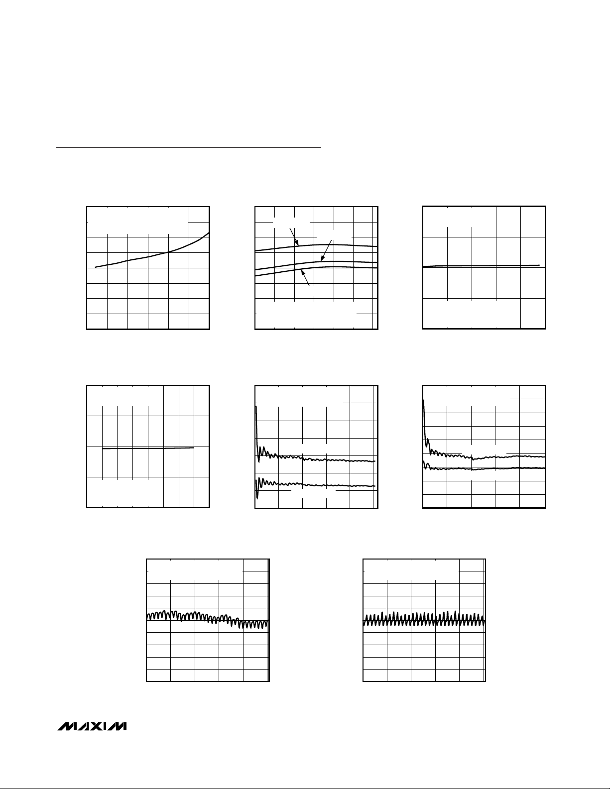
Typical Operating Characteristics
(TA = +25°C, unless otherwise noted.)
SUPPLY CURRENT
vs. SUPPLY VOLTAGE
600
SDA = SCL = THR[3:1] = V
GAIN[3:1] = FS[3:0] = OUT[3:0] = OPEN
575
INP[3:1] = INN[3:1] = GND
550
525
500
475
SUPPLY CURRENT (μA)
450
425
400
2.5 5.5
SUPPLY VOLTAGE (V)
CC
5.04.53.0 3.5 4.0
VOLTCO (SINK)
250
40kΩ LOAD ON FS[3:0].
= +5.5V
V
CC
225
(μA)
200
OUT
I
175
SDA = SCL = THR[3:1] = V
GAIN[3:1] = OPEN
INP[3:1] = INN[3:1] = GND
150
0 4.0
CC
V
(V)
OUT
SUPPLY CURRENT
vs. TEMPERATURE
DS4426 toc01
600
575
550
525
500
475
SUPPLY CURRENT (μA)
450
425
400
VCC = +5.5V
SDA = SCL = THR[3:1] = V
GAIN[3:1] = FS[3:0] = OUT[3:0] = OPEN
INP[3:1] = INN[3:1] = GND
-40
TEMPERATURE (°C)
VCC = +3.3V
VCC = +2.7V
CC
8060-20 0 20 40
DS4426 toc02
-150
-175
(μA)
-200
OUT
I
-225
-250
05
TEMPERATURE COEFFICIENT
vs. SETTING (SOURCE)
DS4426 toc05
650
550
450
350
250
150
50
-50
TEMPERATURE COEFFICIENT (°C/ppm)
-150
-250
0
300
RANGE FOR THE 50μA TO 200μA
CURRENT SOURCE RANGE
250
DS4426 toc04
200
150
100
50
0
TEMPERATURE COEFFICIENT (°C/ppm)
3.53.02.52.01.51.00.5
-50
0
+25°C TO -40°C
+25°C TO +85°C
125100755025
SETTING (DEC)
VOLTCO (SOURCE)
40kΩ LOAD ON FS[3:0].
= +5.5V
V
CC
SDA = SCL = THR[3:1] = V
GAIN[3:1] = OPEN
INP[3:1] = INN[3:1] = GND
CC
V
(V)
OUT
TEMPERATURE COEFFICIENT
vs. SETTING (SINK)
RANGE FOR THE 50μA TO 200μA
CURRENT SINK RANGE
+25°C TO -40°C
+25°C TO +85°C
SETTING (DEC)
DS4426 toc03
4321
DS4426 toc06
125100755025
1.0
INTEGRAL LINEARITY
RANGE FOR THE 50μA TO 200μA
0.8
CURRENT SOURCE AND SINK RANGE
0.6
0.4
0.2
0
INL (LSB)
-0.2
-0.4
-0.6
-0.8
-1.0
0
SETTING (DEC)
125100755025
DS4426 toc07
1.0
0.8
0.6
0.4
0.2
0
DNL (LSB)
-0.2
-0.4
-0.6
-0.8
-1.0
DIFFERENTIAL LINEARITY
RANGE FOR THE 50μA TO 200μA
CURRENT SOURCE AND SINK RANGE
0
SETTING (DEC)
DS4426 toc08
125100755025
Page 6
Detailed Description
The DS4426 contains four I2C-adjustable current
sources that are each capable of sinking and sourcing
current. Three of the current outputs (OUT[3:1]) also
have power-supply tracking circuitry that allows additional current to be sourced during power-up.
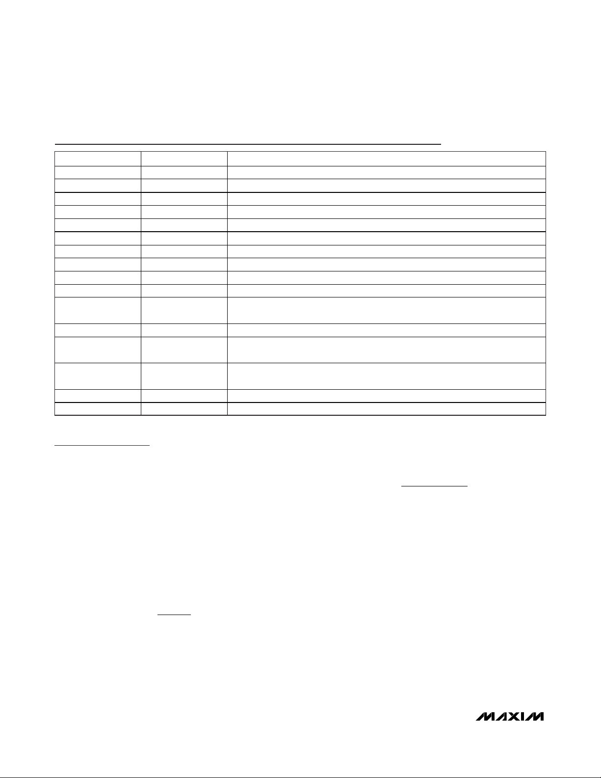
Adjustable Current DACs
Each output (OUT[3:0]) has 127 sink and 127 source
settings that are programmed through the I2C interface.
The full-scale current ranges (and corresponding step
sizes) of the outputs are determined by external resistors connected to the corresponding FS pins (see
Figure 1). The formula to determine the external resistor
values (RFS) for each output is given by:
where IFSis the desired full-scale current value, V
RFS
is
the RFSvoltage (see the
DC Electrical Characteristics
table), and RFSis the external resistor value.
To calculate the output-current value (I
OUT
) based on the
corresponding DAC value (see Table 2 for corresponding memory addresses), use the following equation:
On power-up, the DS4426 current DAC outputs are set
to zero current. This is done to prevent the device from
sinking or sourcing an incorrect current before the system host controller has a chance to modify its setting.
Note, however, that if power-supply tracking is enabled
(see the
Power-Supply Tracking Circuit
section), then
the DS4426 can still source current at power-up.
When used in adjustable power-supply applications
(see Figure 8), the DS4426 does not affect the initial
power-up voltage of the supply because it defaults to
providing zero output current on power-up unless
power-supply tracking is enabled. As it sources or
sinks current into the feedback voltage node, it
changes the amount of output voltage required by the
regulator to reach its steady-state operating point.
DS4426
Quad-Channel, I2C-Margining IDACs with
Three Channels of Power-Supply Tracking
6 _______________________________________________________________________________________
Pin Description
PIN NAME FUNCTION
1 SDA Serial Data Input/Output. I2C data pin.
2 SCL Serial Clock Input. I2C clock input.
3 VCC Voltage Supply
4 OUT0 Current DAC Output
5, 6, 7 OUT1, OUT2, OUT3 Current DAC and Tracking Control Output
8 GND Ground
9 A0 I2C Addre ss Input 0
10 A1 I2C Addre ss Input 1
11, 13, 15 INP1, INP2, INP3 Power-Supply Track ing Pos itive Input
12, 14, 16 INN1, INN2, INN3 Power-Supply Tracking Negati ve Input
17, 19, 20 THR3, THR2, THR1
18 DNC Do Not Connect
21–24 FS0, FS1, FS2, FS3
25, 26, 27
28 N.C. No Connection
— EP Exposed Pad. No connection.
GAIN3, GAIN2,
GAIN1
Threshold Input. Comparator input used to set threshold for tracking
enable/disable based on V
Ful l-Scale Calibration Input. A resistor-to-ground on this input determines fullsca le output current on the associated output.
Gain Adjustment Pin. Connect a resistor between this pin and VCC.
REF
/2.
I
DACValue dec
=×
OUT FS
()
127
V
R
FS
RFS
=
127
I
××16
FS
I
Page 7
DS4426
Quad-Channel, I2C-Margining IDACs with
Three Channels of Power-Supply Tracking
_______________________________________________________________________________________ 7
Using the external resistors R
FS[3:0]
to set the outputcurrent range, the DS4426 provides some flexibility for
adjusting the impedances of the feedback network or
the range over which the power supply can be controlled or margined.
As a source for biasing instrumentation or other circuits,
the DS4426 provides a simple and inexpensive current
source with an I2C interface for control. The adjustable,
full-scale range allows the application to get the most
out of its 7-bit sink or source resolution.
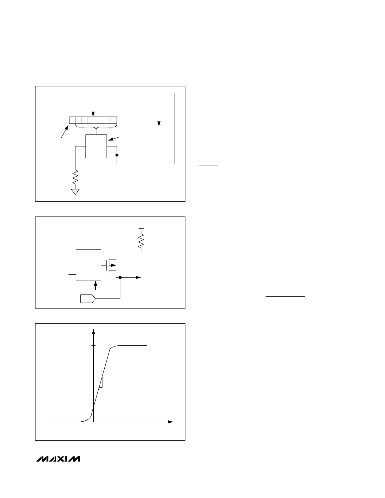
Power-Supply Tracking Circuit
By making use of the power-supply tracking circuitry,
the DS4426 has the ability to source current on powerup. This current is additive with the current DAC
source/sink currents and is determined by the value of
the gain resistor, RG, and the supply voltage, VCC. This
current is controlled by the voltages presented to the
corresponding INP and INN pins, and the voltages presented to the corresponding threshold (THR) pins.
Maximum Source Current
The maximum current the DS4426 can source at
power-up using the power-supply tracking circuitry
depends on the value of the supply voltage, VCC, and
the gain resistor, RG, connected from the corresponding GAIN pin to VCC. The maximum current (I
MAX
) that
can be sourced to the corresponding OUT pin can be
estimated using the following equation:
The power-supply tracking circuit can be estimated
with Figure 2.
Inputs for Power-Supply Tracking:
INP and INN
Each pair of power-supply tracking inputs, INP and
INN, determines if and how much of the I
MAX
current is
sourced when the power-supply tracking circuit is
enabled. When the difference between the voltage presented to INP (V
INP
) and INN (V
INN
) is more than
approximately +0.3V, then the maximum source current, as determined by the value I
MAX
, is sourced into
the OUT pin connection. When the difference between
V
INP
and V
INN
is less than approximately -0.2V, then no
current is sourced into the corresponding OUT pin. The
change in current from no current to I
MAX
can be esti-
mated by the power-supply tracking gain, G
VI
(see the
Power-Supply Tracking Characteristics
table).
Figure 3 shows the typical current behavior of the
power-supply tracking circuit with respect to the voltage difference seen at the INP and INN inputs.
Figure 1. Current DAC Detail
+INP
GAIN
V
CC
DAC
OUT
SLAVE
FEEDBACK
NODE
G
VI
R
G
-INN
SHUTDOWN
Figure 2. Gain Stage
I
-0.2 +0.3
AT V
CC
= +5.0V
I
MAX
G
VI
V
(V
INP
- V
INN
)
Figure 3. INP and INN Differential Inputs
I2C CONTROL
MSB LSB
SOURCE
OR
SINK MODE
R
FS[3:0]
CURRENT
DAC[3:0]
127 POSITIONS
EACH FOR SOURCE
AND SINK MODE
OUT[3:0]FS[3:0]
TRACKING
OUT[3:1] ONLY
VV
−
()
≅
CC OUT
R
G
I
MAX
Page 8

DS4426
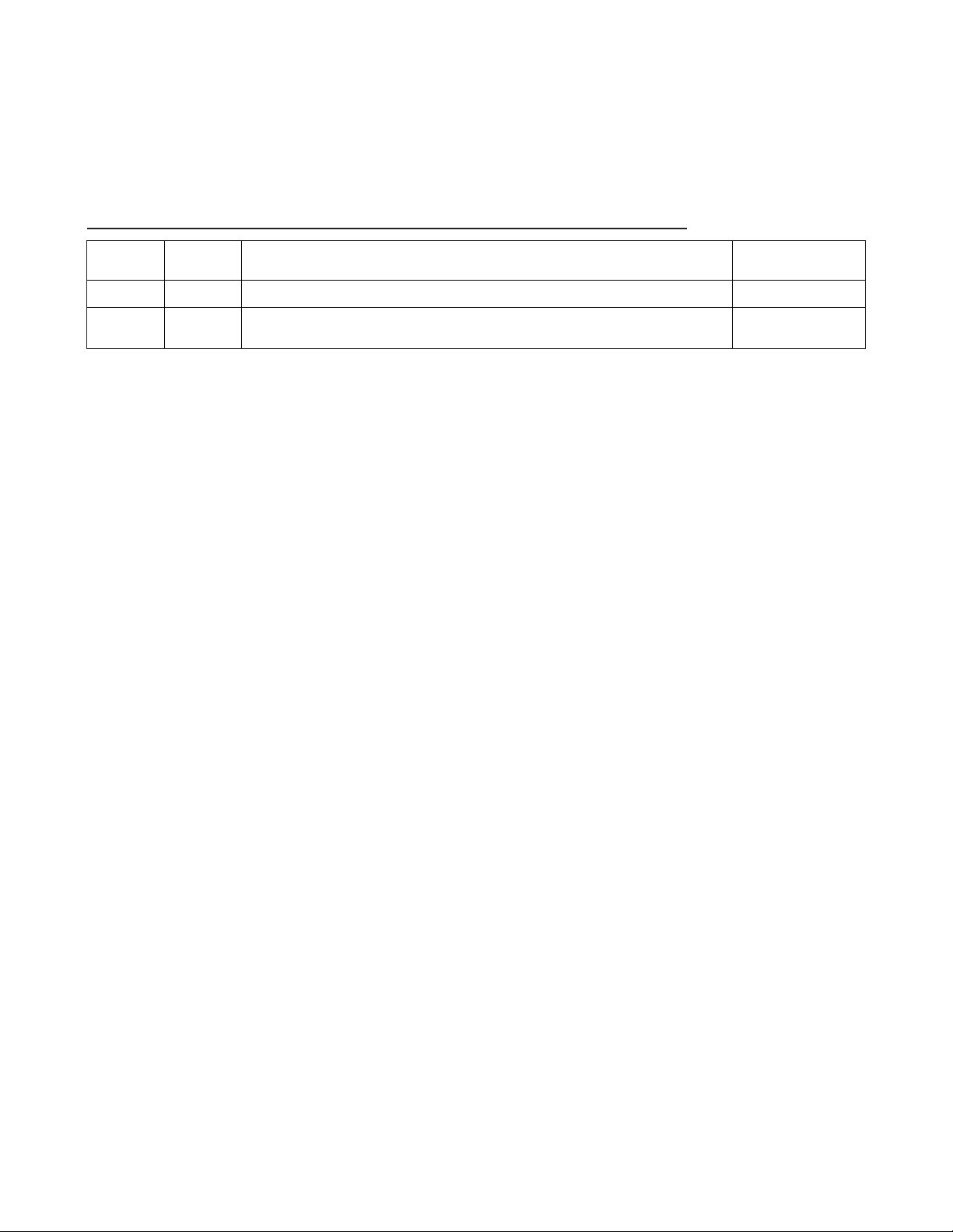
THR Inputs for Enabling
Power-Supply Tracking
Comparators are used to individually enable/disable
power-supply tracking based on the voltage presented
to the corresponding THR pin relative to a fixed internal
reference (V
REF
/2 = +0.62V). Figure 4 shows a typical
startup and shutdown plot based on the voltage presented to the THR pin. Tracking can be disabled by
connecting the corresponding THR pin to a voltage
greater than V
REF
/2. Below this threshold, the tracking
circuit is active.
Power-Supply Tracking in DC-DC
Power Applications
The DS4426 provides several options for power-supply
tracking control of DC-DC power supplies. In many
cases, it is desirable to prevent certain DC-DC supplies
from exceeding the voltage of other supplies. This is
often the case with the voltages applied to a digital
core and I/O. Each DS4426 supports one master with
three slave DC-DCs. See Figure 5 for more information.
Loop Bandwidth Consideration
Power-supply tracking is used to override each slave
DC-DC’s feedback loop during power-up and powerdown. Power-supply tracking is capable of slewing at a
much faster rate than most DC-DC converters. Care
must be exercised when selecting the loop bandwidth
of the master DC-DC, slave DC-DC, and power-supply
tracking control loop such that oscillations and overshoot are minimized.
While the slave DC-DC supplies are tracking the master
DC-DC supply, there are three time constants of concern:
1) Master BW. The master DC-DC control loop bandwidth, power-up ramp rate, and power-down ramp
rate.
2) Slave BW. The slave DC-DC supplies control loop
bandwidths.
3) Tracking BW. The DS4426 tracking circuit bandwidth.
To ensure stable operation and minimize peaking, the
bandwidths should follow the following rule:
Master BW and Slave BW < (Tracking BW/10)
Quad-Channel, I2C-Margining IDACs with
Three Channels of Power-Supply Tracking
8 _______________________________________________________________________________________
Figure 4. Enabling Power-Supply Tracking Using the THR Input
V
V
MASTER
V
V
THRESHOLD
SLAVE
GAIN
ERROR
DS4426 TRACKING DISABLED
TRACKING RANGE: DS4426 OVERRIDES SLAVE'S FEEDBACK LOOP
t
Page 9

Ratiometric Tracking
The DS4426 can maintain a defined ratio between a
slave voltage and the master voltage where:
KSM= V
SLAVE/VMASTER
.
In Figure 5, this ratio is given by the following:
KSM= [R
B[3:1]
/(R
A[3:1]
+ R
B[3:1]
)]/[R
D[3:1]
/(R
C[3:1]
+ R
D[3:1]
)].
Nonratiometric tracking is the special case where KSM= 1.
Power-Supply Tracking Loop Gain Stability
Slave DC-DC output tracking is controlled by the
DS4426 sourcing current into the slave DC-DC's feedback loop. This changes the stability of the loop during
tracking. The amount of gain used can be adjusted by
changing the ratio of R
L/RG
. If oscillations occur,
increasing RGreduces gain and increases the system’s
phase margin. If the slave DC-DC has a compensation
pin, the RC network connected to this pin can also be
adjusted to improve phase margin. This pin is often
labeled COMP or ITH. A larger compensation time constant (increased R and/or increased C) often increases
the stability of the system during tracking; however, this
also modifies the DC-DC's transient response. In order
to prevent modification of the slave DC-DC’s transient
response after power-supply tracking is complete, R
G
should first be modified before adjusting the compensation network. The higher the gain, the less the gain
error. Reducing the gain increases the gain error during
tracking. See Figure 4 for more information.
DS4426
Quad-Channel, I2C-Margining IDACs with
Three Channels of Power-Supply Tracking
_______________________________________________________________________________________ 9
Figure 5. Typical DC-DC Power-Supply Tracking Application
5.0V
0.1μF
10kΩ
2
I
C
10kΩ10kΩ
V
SDA
SCL
A0
A1
CC
V
CC
VOUT
MASTER
REF
1.24V
DC-DC
FS0
CONVERTER
R
FS0
FB
2
C CONTROL
I
INTERFACE
V
REF
OUT0
R
F0
R
E0
x3
INP[3:1]
5.0V
INN[3:1]
GAIN[3:1]
THR[3:1]
R
D[3:1]
V
/2
REF
R
A[3:1]
R
B[3:1]
10kΩ
R
THR[3:1]
R
G[3:1]
R
FS[3:1]
OUT[3:1]
DS4426
R
C[3:1]
FS[3:1]
VOUT
SLAVE
DC-DC
CONVERTER
FB
COMP
R
R
F[3:1]
E[3:1]
Page 10

Inputs for Tracking in DC-DC Power
Applications
When enabling/disabling the power-supply tracking, a
resistor-divider connected to the THR input sets the disable threshold (see V
THRESHOLD
in Figure 4). The top
of the resistor-divider must be connected to the master
DC-DC voltage for correct operation. Below this threshold, the tracking circuit is active.
Power-Supply Sequencing
The DS4426 can be used to perform power-supply
sequencing. This is a subset of power-supply tracking
with modifications to the external resistor network. The
basic concept is that the DS4426 sources maximum
current into the slave power supply's feedback node
until a voltage in the system has risen above a specific
voltage level. By sourcing the maximum current into the
feedback node, the power supply's output is held off.
Maximum sourcing current is achieved with two steps:
1) Apply the maximum allowed input voltage across
INP and INN. Connect INP to VCC- 1.4V using a
voltage-divider to ground. Connect INN to ground.
2) Set the gain to the maximum allowed (RL/RG= 5).
The slave power supply is allowed to turn on once the
voltage on THR is greater than V
REF
/2. Use a resistordivider connected to the rising system voltage to scale
the trip point to V
REF
/2.
I2C Slave Address
The DS4426 responds to one of four I2C slave addresses determined by the state of the input on the two
address inputs. The two input states are connected to
VCCor connected to ground.
Memory Organization
The DS4426’s current sources are controlled by writing
to memory addresses listed in Table 2.
The format of each of the output control registers is
given by:
where:
For example:
R
FS0
= 80kΩ and register 0xF8h is written to a value of
0xAAh. Use the following formula to calculate the output current:
I
FS
= (1.0V/80kΩ) x (127/16) = 99.22µA
The MSB of the output register is 1, so the output is
sourcing the value corresponding to position 2Ah (42
decimal). The magnitude of the output current is equal
to the following:
99.22µA x (42/127) = 32.8125µA
DS4426
Quad-Channel, I2C-Margining IDACs with
Three Channels of Power-Supply Tracking
10 ______________________________________________________________________________________
Table 1. Slave Addresses
Table 2. Memory Addresses
A1 A0 SLAVE ADDRESS (HEX)
GND GND 90h
GND VCC 92h
VCC GND 94h
VCC V
96h
CC
MEMORY ADDRESS (HEX) CURRENT SOURCE
F8h OUT0
F9h OUT1
FAh OUT2
FBh OUT3
BIT 7
(MSB)
BIT 6 BIT 5 BIT 4 BIT 3 BIT 2 BIT 1
S D6 D5 D4 D3 D2 D1 D
BIT NAME DESCRIPTION
Determines if DAC source s or
Sign
S
DXData
sinks current. For sink, S = 0.
Bit
For source, S = 1.
7-bit data word controlling DAC
output. Setting 0000000b
outputs zero current regardles s
of the state of the sign bit.
BIT 0
(LSB)
0
POWER-ON
DEFAULT
0b
0000000b
Page 11

I2C Serial Interface Description
I2C Definitions
The following terminology is commonly used to
describe I
2
C data transfers:
I2C Slave Address: The slave address of the
DS4426 is determined by the state of the A0 and A1
pins (see Table 1).
Master Device: The master device controls the slave
devices on the bus. The master device generates
SCL clock pulses and START and STOP conditions.
Slave Devices: Slave devices send and receive
data at the master’s request.
Bus Idle or Not Busy: Time between STOP and
START conditions when both SDA and SCL are inactive and in their logic-high states. When the bus is
idle it often initiates a low-power mode for slave
devices.
START Condition: A START condition is generated
by the master to initiate a new data transfer with a
slave. Transitioning SDA from high to low while SCL
remains high generates a START condition. See
Figure 3 for applicable timing.
STOP Condition: A STOP condition is generated by
the master to end a data transfer with a slave.
Transitioning SDA from low to high while SCL
remains high generates a STOP condition. See
Figure 3 for applicable timing.
Repeated START Condition: The master can use a
repeated START condition at the end of one data
transfer to indicate that it will immediately initiate a
new data transfer following the current one.
Repeated STARTs are commonly used during read
operations to identify a specific memory address to
begin a data transfer. A repeated START condition
is issued identically to a normal START condition.
See Figure 6 for applicable timing.
Bit Write: Transitions of SDA must occur during the
low state of SCL. The data on SDA must remain valid
and unchanged during the entire high pulse of SCL,
plus the setup-and-hold time requirements (Figure
6). Data is shifted into the device during the rising
edge of the SCL.
Bit Read: At the end of a write operation, the master
must release the SDA bus line for the proper amount
of setup time (Figure 6) before the next rising edge
of SCL during a bit read. The device shifts out each
bit of data on SDA at the falling edge of the previous
SCL pulse, and the data bit is valid at the rising
edge of the current SCL pulse. Remember that the
master generates all SCL clock pulses, including
when it is reading bits from the slave.
Acknowledgement (ACK and NACK): An
Acknowledgement (ACK) or Not Acknowledge
(NACK) is always the ninth bit transmitted during a
byte transfer. The device receiving data (the master
during a read or the slave during a write operation)
performs an ACK by transmitting a zero during the
ninth bit. A device performs a NACK by transmitting
a 1 during the ninth bit. Timing for the ACK and
NACK is identical to all other bit writes (Figure 6). An
ACK is the acknowledgment that the device is properly receiving data. A NACK is used to terminate a
read sequence or as an indication that the device is
not receiving data.
Byte Write: A byte write consists of 8 bits of information transferred from the master to the slave (most
significant bit first) plus a 1-bit acknowledgement
from the slave to the master. The 8 bits transmitted
by the master are done according to the bit-write definition, and the acknowledgement is read using the
bit-read definition.
Byte Read: A byte read is an 8-bit information transfer from the slave to the master plus a 1-bit ACK or
NACK from the master to the slave. The 8 bits of
information that are transferred (most significant bit
first) from the slave to the master are read by the
master using the bit-read definition, and the master
transmits an ACK using the bit-write definition to
receive additional data bytes. The master must
NACK the last byte read to terminate communication
so the slave returns control of SDA to the master.
Slave Address Byte: Each slave on the I
2
C bus
responds to a slave address byte sent immediately
following a START condition. The slave address byte
contains the slave address in the most significant 7
bits and the R/W bit in the least significant bit. The
DS4426’s slave address is determined by the state
of the A0 and A1 pins (see Table 1). When the R/W
bit is 0 (such as in 90h), the master is indicating it
will write data to the slave. If R/W = 1 (91h in this
case), the master is indicating it wants to read from
the slave. If an incorrect slave address is written, the
DS4426 assumes the master is communicating with
another I2C device and ignores the communication
until the next START condition is sent.
Memory Address: During an I2C write operation,
the master must transmit a memory address to identify the memory location where the slave is to store
the data. The memory address is always the second
byte transmitted during a write operation following
the slave address byte.
DS4426
Quad-Channel, I2C-Margining IDACs with
Three Channels of Power-Supply Tracking
______________________________________________________________________________________ 11
Page 12

DS4426
I2C Communication
Writing to a Slave: The master must generate a START
condition, write the slave address byte (R/W = 0), write
the memory address, write the byte of data, and generate a STOP condition. Remember that the master must
read the slave’s acknowledgement during all byte-write
operations.
Reading from a Slave: To read from the slave, the
master generates a START condition, writes the slave
address byte with R/W = 1, reads the data byte with a
NACK to indicate the end of the transfer, and generates
a STOP condition.
Quad-Channel, I2C-Margining IDACs with
Three Channels of Power-Supply Tracking
12 ______________________________________________________________________________________
Figure 7. I2C Communication Examples
SCL
NOTE: TIMING IS REFERENCED TO V
IL(MAX)
AND V
IH(MIN)
.
SDA
STOP START REPEATED
START
t
BUF
t
HD:STA
t
HD:DAT
t
SU:DAT
t
SU:STO
t
HD:STA
t
SP
t
SU:STA
t
HIGH
t
R
t
F
t
LOW
Figure 6. I2C Timing Diagram
2
C WRITE TRANSACTION
TYPICAL I
MSB LSB MSB LSB MSB LSB
START
1 0 0 1 0 A1 A0 R/W
SLAVE
b7 b6 b5 b4 b3 b2 b1 b0
ACK
SLAVE
b7 b6 b5 b4 b3 b2 b1 b0
ACK
SLAVE
ACK
STOP
SLAVE
ADDRESS*
2
EXAMPLE I
C TRANSACTIONS (WHEN A0 AND A1 ARE GROUNDED)
SINGLE-BYTE WRITE
A)
-WRITE REGISTER F9h TO 00h
SINGLE-BYTE READ
B)
-READ REGISTER F8h
*THE SLAVE ADDRESS IS DETERMINED BY ADDRESS PINS A0 AND A1.
START
START
READ/
WRITE
90h F9h
10010000 11111 001 00000000
90h
SLAVE
ACK
SLAVE
ACK
REGISTER/MEMORY ADDRESS
F8h
DATA
SLAVE
ACK
SLAVE
ACK
REPEATED
START
SLAVE
STOP
ACK
91h
10010 001
SLAVE
ACK
DATA
MASTER
NACK
STOP10010000 11111 000
Page 13

Applications Information
Example Calculations for an Adjustable
Power Supply
In this example, the circuit shown in Figure 8 is used to
margin a +2.0V supply by ±20%. The margined power
supply has a DC-DC converter output voltage, V
OUT
, of
+2.0V and a DC-DC converter feedback voltage, V
FB
,
of +0.8V. To determine the relationship of R
0A
and R0B,
start with the equation:
Substituting VFB= +0.8V and V
OUT
= +2.0V, the rela-
tionship between R
0A
and R0Bis determined to be:
R0A= 1.5 x R
0B
I
OUT0
is chosen to be 100µA (midrange source/sink
current for the DS4426). Summing the currents into the
feedback node, we have the following:
I
OUT0
= I
R0B
- I
R0A
where:
and
To create a ±20% margin in the supply voltage, the
value of V
OUT
is set to +2.4V. With these values in
place, R0Bis calculated to be 2.67kΩ, and R0Ais
DS4426
Quad-Channel, I2C-Margining IDACs with
Three Channels of Power-Supply Tracking
______________________________________________________________________________________ 13
Figure 8. Example Typical Application Circuit
R
0
V
=
FB
B
RR
+
00
AB
V
×
OUT
4.7kΩ4.7kΩ
SDA
SCL
GND
V
CC
DS4426
OUT0
V
I
RB
FB
=
R
B00
VV
−
I
RA
OUT FB
=
R
A00
V
CC
DC-DC
CONVERTER
OUT
FB
V
= 2.0V*
OUT
I
I
R0A
R0B
R0A = 4kΩ
VFB = 0.8V*
R0B = 2.67kΩ
*V
AND VFB VALUES ARE DETERMINED BY THE DC-DC CONVERTER AND SHOULD NOT BE CONFUSED WITH V
OUT
FS0
R
FS0
= 80kΩ
I
OUT0
OUT
AND V
OF THE DS4426.
REF
Page 14

DS4426
Quad-Channel, I2C-Margining IDACs with
Three Channels of Power-Supply Tracking
14 ______________________________________________________________________________________
calculated to be 4.00kΩ. The current DAC in this configuration allows the output voltage to be moved linearly
from +1.6V to +2.4V using 127 settings. This corresponds to a resolution of 6.3mV/step.
V
CC
Decoupling
To achieve the best results when using the DS4426,
decouple the power supply with a 0.01µF (or 0.1µF)
capacitor. Use a high-quality, ceramic, surface-mount
capacitor if possible. Surface-mount components minimize lead inductance, which improves performance.
Ceramic capacitors tend to have adequate high-frequency response for decoupling applications.
DS4426
SDA
V
CC
SCL
A0
A1
FS0
OUT0
I
2
C CONTROL
INTERFACE
V
CC
V
REF
REF
1.24V
INP1
FS1
OUT1
INN1
THR1
GAIN1
V
REF
/2
INP2
FS2
OUT2
INN2
THR2
GAIN2
V
REF
/2
INP3
FS3
OUT3
INN3
THR3
GND
GAIN3
V
REF
/2
Functional Diagram
Package Information
For the latest package outline information and land patterns, go
to www.maxim-ic.com/packages
.
PACKAGE TYPE PACKAGE CODE DOCUMENT NO.
28 TQFN T2844+1
21-0139
Page 15
DS4426
Quad-Channel, I2C-Margining IDACs with
Three Channels of Power-Supply Tracking
Maxim cannot assume responsibility for use of any circuitry other than circuitry entirely embodied in a Maxim product. No circuit patent licenses are
implied. Maxim reserves the right to change the circuitry and specifications without notice at any time.
Maxim Integrated Products, 120 San Gabriel Drive, Sunnyvale, CA 94086 408-737-7600 ____________________
15
© 2009 Maxim Integrated Products Maxim is a registered trademark of Maxim Integrated Products, Inc.
Revision History
REVISION
NUMBER
0 4/08 Initial release. —
1 7/09
REVISION
DATE
DESCRIPTION
Added OUT[3:0] to the Absolute Maximum Ratings for the following condition:
Voltage Range on A0, A1, FS[3:0], GAIN[3:1], INN[3:1], INP[3:1], and THR[3:1].
PAGES
CHANGED
2
 Loading...