

Page 1
DS3690
3.3V 26-Channel, Three-Stateable
Transmission Gate
________________________________________________________________
Maxim Integrated Products
1
For pricing, delivery, and ordering information, please contact Maxim Direct at 1-888-629-4642,
or visit Maxim’s website at www.maxim-ic.com.
General Description
The DS3690 is a 26-channel, three-stateable transmission gate designed for transparent digital signal transfer when enabled and fast-gated bus isolation when the
device is disabled. Each of the 26 independent channels can be used for input, output, or I/O signal applications, with a typical signal propagation delay of less
than 10ns. Using the logic-control input, all channels
can be simultaneously enabled for bus transmission or
forced to a high-impedance condition to isolate a critical component on that bus.
The DS3690 operates on a single 3.3V (typical) power
supply and is available in a space-saving 56-pin leadfree TQFN package.
Applications
POS Terminals
PIN Pads
Cryptographic Processors
Gaming
Lottery Terminals
Industrial Controls and Monitoring
Features
♦ 26 Bidirectional Channels
♦ Low Propagation Delay (< 10ns typ)
♦ High-Speed On/Off Time (< 20ns typ)
♦ 2.7V to 3.6V Supply
♦ Wide Temperature Range: -55°C to +85°C
♦ TQFN Package (5mm x 11mm x 0.8mm)
Ordering Information
Rev 0; 10/07
+
Denotes a lead-free package.
TRL = Tape and reel.
×
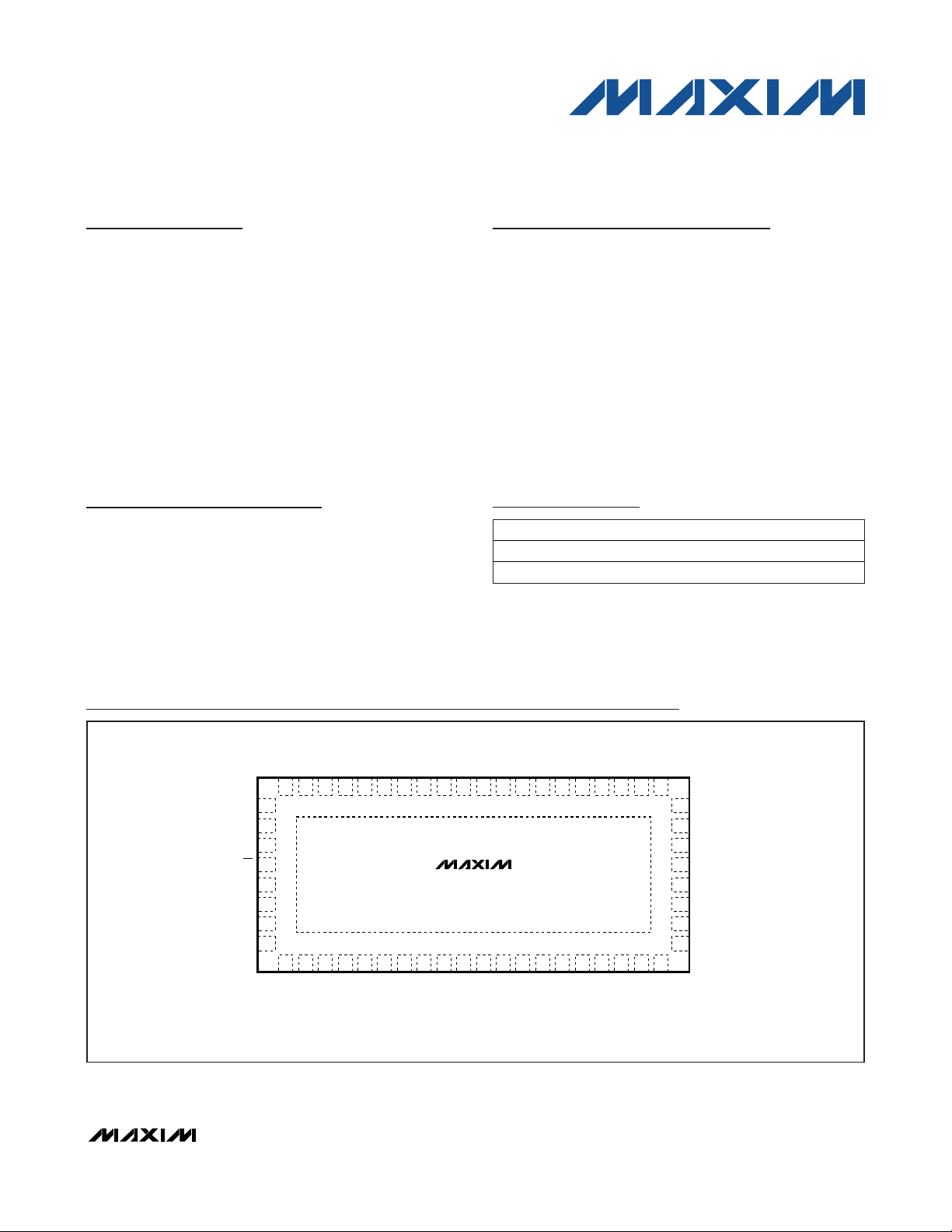
Pin Configuration
Typical Operating Circuit appears at end of data sheet.
PART TEMP RANGE PIN-PACKAGE
DS3690T+ -55°C to +85°C 56 TQFN
DS3690T+TRL -55°C to +85°C 56 TQFN
TOP VIEW
CH10B37CH12B36CH13B35CH14B
CH11B
CH24B
CH25B
CH26B
GND
CH26A
CH25A
CH24A
CH09B
CH05B42CH07B
CH04B
CH03B
CH02B
CH01B
44
43
45
46
47
48
49
50
51
CE
52
53
54
55
+
56
5
4
3
2
1
CH05A7CH07A
CH04A
CH03A
CH02A
CH01A
CH08B
CH06B
40
41
DS3690
EXPOSED PAD (ON BOTTOM)
9
8
6
CH09A
CH08A
CH06A
39
38
10
11
CH10A12CH12A13CH13A14CH14A
CH11A
CH16B31CH18B30CH19B29CH20B
CH15B
33
34
16
15
CH16A18CH18A19CH19A20CH20A
CH15A
TQFN
11mm × 0.8mm)
(5mm
32
17
CH17B
CH17A
28
CH21B
27
CH22B
26
CH23B
25
GND
24
V
CC
23
CH23A
22
CH22A
21
CH21A
Page 2
DS3690
3.3V 26-Channel, Three-Stateable
Transmission Gate
2 _______________________________________________________________________________________
ABSOLUTE MAXIMUM RATINGS
RECOMMENDED OPERATING CONDITIONS
(TA= -55°C to +85°C)
Stresses beyond those listed under “Absolute Maximum Ratings” may cause permanent damage to the device. These are stress ratings only, and functional
operation of the device at these or any other conditions beyond those indicated in the operational sections of the specifications is not implied. Exposure to
absolute maximum rating conditions for extended periods may affect device reliability.
Voltage Range on Any Pin Relative to Ground......-0.5V to +6.0V
Operating Temperature Range ...........................-55°C to +85°C
Storage Temperature Range .............................-55°C to +125°C
Soldering Temperature...................Refer to IPC/JEDEC J-STD-020
DC ELECTRICAL CHARACTERISTICS
(VCC= +2.7V to +3.6V, TA= -55°C to +85°C, unless otherwise noted.)
AC ELECTRICAL CHARACTERISTICS
(VCC= +2.7V to +3.6V, TA= -55°C to +85°C, unless otherwise noted.)
Input Pulse Levels: VIL= 0.0V, VIH= 2.7V
Input Pulse Rise and Fall Times: 5ns
Input and Output Timing Reference Level: V
CC
/2
Output Load: C
L
(100pF)
AC TEST CONDITIONS
PARAMETER SYMBOL CONDITIONS MIN TYP MAX UNITS
Supply Voltage V
Input Logic 1 V
Input Logic 0 V
PARAMETER S YMBOL CONDITIONS MIN TYP MAX UNITS
Standby Current I
Input Leakage Current (CE) II VIN = 0V to VCC, TA = +25°C -0.1 +0.1 μA
I/O Leakage Current I
CC
(Note 1) 2.7 3.3 3.6 V
CC
(Note 1)
IH
(Note 1) -0.3
IL
CE = CH1 CH26 = VCC, I
CE = VIH -1.0 +1.0 μA
IO
= 0mA 1 μA
OUT
0.7 x
V
CC
VCC +
0.3
0.3 x
V
CC
V
V
PARAMETER S YMBOL CONDITIONS MIN TYP MAX UNITS
Propagation De lay
(A to B or B to A)
Chip Enable to Output Valid t
Chip Enable to Output Deselect t
Input to CE Setup Time tIS (Note 4) 0 ns
Skew Between Channels tS (Notes 5, 6) 1 ns
t
CEV
CEZ
CE = VIL (Note 2) 10 ns
PD
(Notes 2, 3) 20 ns
(Notes 2, 3) 20 ns
Page 3
DS3690
3.3V 26-Channel, Three-Stateable
Transmission Gate
_______________________________________________________________________________________ 3
Note 1: All voltages referenced to ground.
Note 2: Typical waveform shown is labeled CHxxA (input) to CHxxB (output), and is identical in function when selecting pin CHxxB
(as the input) to pin CHxxA (as the output).
Note 3: Output reference level is V
CC
/2.
Note 4: Input transitions prior to the CE falling edge are ignored (don’t care).
Note 5: Propagation delay differential between any two channels when using a common input signal source.
Note 6: Guaranteed by design and not 100% tested.
CAPACITANCE
(TA= +25°C)
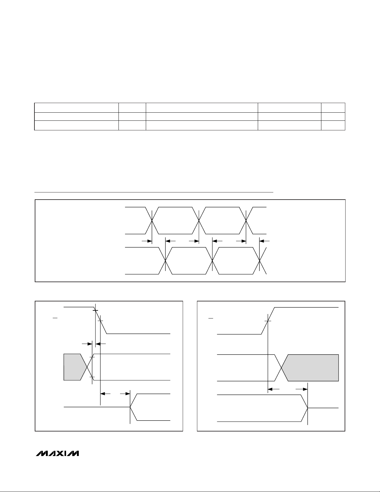
Timing Diagrams
CHxxA
CHxxB
t
PD
t
PD
t
PD
Figure 1. Digital Channel Propagation Delay
Figure 2. Digital Channels Enabled by CE
Figure 3. Digital Channels Disabled by CE
PARAMETER S YMBOL CONDITIONS MIN TYP MAX UNITS
Input Capacitance (CE) CIN Not production tested 5 pF
I/O Capacitance CIO Not production tested 8 pF
CE
t
IS
CHxxA
CHxxB
DON'T
CARE
HIGH IMPEDANCE
t
CEV
CE
CHxxA
CHxxB
DON'T CARE
t
CEZ
HIGH IMPEDANCE
Page 4

DS3690
3.3V 26-Channel, Three-Stateable
Transmission Gate
4 _______________________________________________________________________________________
Typical Operating Characteristics
(VCC= 3.3V, TA= +25°C, unless otherwise noted.)
POWER-SUPPLY CURRENT
vs. INPUT VOLTAGE
DS3690 toc01
INPUT VOLTAGE (V)
SUPPLY CURRENT (A)
3.22.92.32.0 2.6
1.E-09
1.E-08
1.E-07
1.E-06
1.E-05
1.E-04
1.E-03
1.E-02
1.E-10
CE = CH1A–CH26A,
CH1B–CH26B = FLOAT
T
A
= +85°CTA = +85°C
TA = +25°CTA = +25°C
TA = -55°CTA = -55°C
CHANNEL ON-RESISTANCE CHANGE
vs. INPUT VOLTAGE
DS3690 toc02
INPUT VOLTAGE (V)
DELTA RESISTANCE (Ω)
2.62.01.30.7
5
10
15
20
25
0
0.0 3.3
I
OUT
= -0.1mA, CH1
OUTPUT-VOLTAGE HIGH
vs. OUTPUT CURRENT
DS3690 toc03
OUTPUT CURRENT (mA)
OUTPUT VOLTAGE (V)
-1-2-3-4
2.7
2.8
2.9
3.0
3.1
3.2
2.6
-5 0
VIN = +3.0V, CH1A–CH1B
OUTPUT-VOLTAGE LOW
vs. OUTPUT CURRENT
DS3690 toc04
OUTPUT CURRENT (mA)
OUTPUTVOLTAGE (V)
4321
0.1
0.2
0.3
0.4
0.5
0.6
0.0
05
VIN = +0.3V, CH1A–CH1B
Page 5

DS3690
3.3V 26-Channel, Three-Stateable
Transmission Gate
_______________________________________________________________________________________ 5
Pin Description
PIN NAME FUNCTION
1 CH01A Channel 1 Terminal A
2 CH02A Channel 2 Terminal A
3 CH03A Channel 3 Terminal A
4 CH04A Channel 4 Terminal A
5 CH05A Channel 5 Terminal A
6 CH06A Channel 6 Terminal A
7 CH07A Channel 7 Terminal A
8 CH08A Channel 8 Terminal A
9 CH09A Channel 9 Terminal A
10 CH10A Channel 10 Terminal A
11 CH11A Channel 11 Terminal A
12 CH12A Channel 12 Terminal A
13 CH13A Channel 13 Terminal A
14 CH14A Channel 14 Terminal A
15 CH15A Channel 15 Terminal A
16 CH16A Channel 16 Terminal A
17 CH17A Channel 17 Terminal A
18 CH18A Channel 18 Terminal A
19 CH19A Channel 19 Terminal A
20 CH20A Channel 20 Terminal A
21 CH21A Channel 21 Terminal A
22 CH22A Channel 22 Terminal A
23 CH23A Channel 23 Terminal A
24 VCC Supply Voltage
25, 53 GND Ground
26 CH23B Channel 23 Terminal B
27 CH22B Channel 22 Terminal B
28 CH21B Channel 21 Terminal B
29 CH20B Channel 20 Terminal B
PIN NAME FUNCTION
30 CH19B Channel 19 Terminal B
31 CH18B Channel 18 Terminal B
32 CH17B Channel 17 Terminal B
33 CH16B Channel 16 Terminal B
34 CH15B Channel 15 Terminal B
35 CH14B Channel 14 Terminal B
36 CH13B Channel 13 Terminal B
37 CH12B Channel 12 Terminal B
38 CH11B Channel 11 Terminal B
39 CH10B Channel 10 Terminal B
40 CH09B Channel 9 Terminal B
41 CH08B Channel 8 Terminal B
42 CH07B Channel 7 Terminal B
43 CH06B Channel 6 Terminal B
44 CH05B Channel 5 Terminal B
45 CH04B Channel 4 Terminal B
46 CH03B Channel 3 Terminal B
47 CH02B Channel 2 Terminal B
48 CH01B Channel 1 Terminal B
49 CH24B Channel 24 Terminal B
50 CH25B Channel 25 Terminal B
51 CH26B Channel 26 Terminal B
52 CE Chip-Enable Input (Active Low)
54 CH26A Channel 26 Terminal A
55 CH25A Channel 25 Terminal A
56 CH24A Channel 24 Terminal A
— EP
Exposed Paddle. Must be
connected to ground.
Page 6

DS3690
Detailed Description
The DS3690 is a 26-channel, noninverting, bidirectional
CMOS transmission gate, and is intended for use in
applications where a downstream component must be
isolated from a common control, address, or data bus in
a timely fashion. Each of the 26 independent channels
can be used for input, output, or I/O signal applications.
The chip-enable input (CE) allows gated bus control for
either signal transmission or bus isolation.
Each independent channel consists of two pins
(“CHxxA” and “CHxxB” where xx is 01–26). Since all 26
channels are capable of bidirectional function, either
CHxxA or CHxxB can be selected as the input pin for
any unidirectional signal requirements. A change of
logic state on one side of any channel is directly reflected on the other side of that channel. Signal
propagation delay (CHxxA to CHxxB, or CHxxB to
CHxxA) is illustrated in Figure 1 as tPD.
All channels can be simultaneously enabled or forced
to a high-impedance state using the CE input. When CE
becomes a logic zero, all channels are enabled for
signal transmission within t
CEV
(see Figure 2). When CE
becomes a logic one, all channels are forced to a
high-impedance state within t
CEZ
(see Figure 3).
Applications Information
Power-Supply Decoupling
To achieve the best results when using the DS3690,
decouple the power supply with a 0.1µF capacitor.
Use a high-quality, ceramic surface-mount capacitor if
possible. Surface-mount components minimize lead
inductance, which improves performance, while ceramic capacitors have adequately high-frequency
response for decoupling applications.
Pin Connections
For optimum circuit operation, connect pins 25 and 53 to
a common ground. The exposed pad on the package
bottom side should be connected to ground.
To prevent an unused transmission channel from generating any undesired activity, it is recommended that one
side of that unused channel be connected to ground
(either the A or B terminal, at the designer’s discretion).
3.3V 26-Channel, Three-Stateable
Transmission Gate
6 _______________________________________________________________________________________
Typical Operating Circuit
MICRO
R/W CONTROL
ADDRESS (A
I/O (DQ
0–X
BUS ENABLE
0–X
+3.3V
R/W CONTROL
)
)
DS3690
CE
ADDRESS (A
I/O (DQ
0–X
0–X
)
)
EXTERNAL
MEMORY
Page 7

DS3690
3.3V 26-Channel, Three-Stateable
Transmission Gate
Maxim cannot assume responsibility for use of any circuitry other than circuitry entirely embodied in a Maxim product. No circuit patent licenses are
implied. Maxim reserves the right to change the circuitry and specifications without notice at any time.
Maxim Integrated Products, 120 San Gabriel Drive, Sunnyvale, CA 94086 408-737-7600 _____________________
7
© 2007 Maxim Integrated Products is a registered trademark of Maxim Integrated Products, Inc.
Functional Diagram Package Information
(For the latest package outline information, go to
www.maxim-ic.com/DallasPackInfo
.)
PACKAGE TYPE DOCUMENT NO.
56 TQFN
21-0187
V
CC
V
CC
CE
CH01BCH01A
CH02BCH02A
CH03BCH03A
GND
CH26A
DS3690
CH26B
 Loading...