

Page 1
General Description
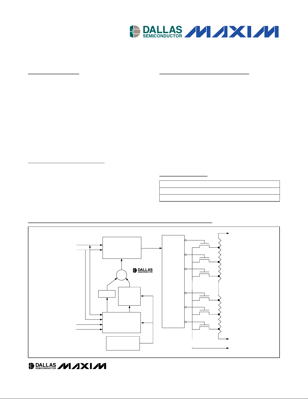
The DS3501 is a 7-bit, nonvolatile (NV) digital potentiometer featuring an output voltage range of up to 15.5V.
Programming is accomplished by an I
2
C-compatible
interface, which can operate at speeds of up to 400kHz.
External voltages are applied at the RL and RH inputs to
define the lowest and highest potentiometer outputs.
The DS3501 contains an on-chip temperature sensor
and associated analog-to-digital converter (ADC). The
ADC output addresses a 36-word NV lookup table
(LUT). The LUT output can drive the pot directly or be
added to an NV initial-value register (IVR) to drive the
pot. This flexible LUT-based architecture allows the
DS3501 to provide a temperature-compensated potentiometer output with arbitrary slope.
Applications
TFT-LCD V
COM
Calibration
Linear and Nonlinear Compensation
Instrumentation and Industrial Controls
Mechanical POT Replacement
Optical Transceivers
Features
♦ 128 Wiper Tap Points
♦ Full-Scale Resistance: 10kΩ
♦ On-Chip Temperature Sensor and ADC
♦ 36-Byte Lookup Table (LUT)
♦ I
2
C-Compatible Serial Interface
♦ Address Pins Allow Up to Four DS3501s to Share
the Same I
2
C Bus
♦ Digital Operating Voltage: 2.7V to 5.5V
♦ Analog Operating Voltage: 4.5V to 15.5V
♦ Operating Temperature: -40°C to +100°C
♦ Pin and Software Compatible with ISL95311
(Default Mode)
♦ 10-Pin μSOP Package
DS3501
High-Voltage, NV, I2C POT with Temp Sensor
and Lookup Table
______________________________________________
Maxim Integrated Products
1
Rev 0; 1/07
+
Denotes a lead-free package.
T&R denotes tape-and-reel.
Ordering Information
VOLATILE
WIPER REGISTER
NV IVR
36-BYTE
LUT
NV
MEMORY
CONTROL
CIRCUITRY
AND ADDRESS
DECODE
TEMP
SENSOR
AND ADC
A1
A0
SDA
SCL
∑
DECODER
LEVEL
SHIFTER
127
126
125
2
1
0
RH
RL
RW
DS3501
Functional Diagram
Pin Configuration and Typical Operating Circuit appear at
end of data sheet.
For pricing, delivery, and ordering information, please contact Maxim/Dallas Direct! at
1-888-629-4642, or visit Maxim’s website at www.maxim-ic.com.
PART TEMP RANGE PIN-PACKAGE
DS3501U+ -40°C to +100°C 10 µSOP
DS3501U+T&R -40°C to +100°C 10 µSOP
Page 2
DS3501
High-Voltage, NV, I2C POT with Temp Sensor
and Lookup Table
2 _____________________________________________________________________
ABSOLUTE MAXIMUM RATINGS
RECOMMENDED OPERATING CONDITIONS
(TA= -40°C to +100°C)
Stresses beyond those listed under “Absolute Maximum Ratings” may cause permanent damage to the device. These are stress ratings only, and functional
operation of the device at these or any other conditions beyond those indicated in the operational sections of the specifications is not implied. Exposure to
absolute maximum rating conditions for extended periods may affect device reliability.
Voltage Range on VCCRelative to GND ...............-0.5V to +6.0V
Voltage Range on V+ Relative to GND ..................-0.5V to +17V
Voltage Range on SDA, SCL, A0, A1
Relative to GND..........-0.5V to (V
CC
+ 0.5V), not to exceed 6.0V
Voltage Range on RH, RL, RW...................................-0.5V to V+
Voltage Range Across RH and RL Pins .....................-0.5V to V+
Operating Temperature Range .........................-40°C to +100°C
Programming Temperature Range .........................0°C to +70°C
Storage Temperature Range .............................-55°C to +125°C
Soldering Temperature .......................................See IPC/JEDEC
J-STD-020 Specification
Maximum RW Current ...........................................................1mA
DC ELECTRICAL CHARACTERISTICS
(VCC= +2.7V to +5.5V, TA= -40°C to +100°C, unless otherwise noted.)
PARAMETER SYMBOL CONDITIONS MIN TYP MAX UNITS
Supply Voltage V
V+ Voltage V+ V+ > V
Input Logic 1
(SCL, SDA, A0, A1)
Input Logic 0
(SCL, SDA, A0, A1)
Resistor Inputs (RL, RW, RH) V
Wiper Current I
V
V
RES
WIPER
(Note 1) +2.7 +5.5 V
CC
CC
IH
IL
+4.5 +15.5 V
0.7 x
V
CC
-0.3
-0.3
V
CC
+ 0.3
0.3 x
V
CC
V+
+ 0.3
1mA
V
V
V
PARAMETER SYMBOL CONDITIONS MIN TYP MAX UNITS
I
VCC Supply Current
Standby Supply Current I
V+ Bias Current I
Inp ut Leakag e ( S D A, S C L, A0, A1) I
Low-Level Output Voltage (SDA) V
I/O Capacitance C
Power-Up Recall Voltage V
Power-Up Memory Recall Delay t
Wiper Resistance R
E nd - to- E nd Resi stance ( RH to RL) R
R
Tolerance TA = +25°C -20 +20 %
TOTAL
R
Temp Co. (Note 7) ±200 ppm
TOTAL
CH, CL, CW Capacitance C
CC
I
CC2
STBY
V+
POR
TOTAL
POT
(Note 2) 2 mA
(Note 3) 250 350 µA
(Note 4) 40 60 µA
L
3mA sink current 0.0 0.4 V
OL
I/O
(Note 5) 1.6 2.6 V
(Note 6) 5 ms
D
V+ = 15.0V 5000 Ω
W
+1 µA
-1 +1 µA
510pF
10 kΩ
10 pF
Page 3
DS3501
High-Voltage, NV, I2C POT with Temp Sensor
and Lookup Table
_____________________________________________________________________ 3
ANALOG VOLTAGE MONITORING CHARACTERISTICS
(VCC= +2.7V to +5.5V, TA= -40°C to +100°C, unless otherwise noted.)
TEMPERATURE SENSOR CHARACTERISTICS
(VCC= +2.7V to +5.5V, TA= -40°C to +100°C, unless otherwise noted.)
VOLTAGE-DIVIDER CHARACTERISTICS
(VCC= +2.7V to +5.5V, TA= -40°C to +100°C, unless otherwise noted.)
I2C AC ELECTRICAL CHARACTERISTICS
(VCC= +2.7V to +5.5V, TA= -40°C to +100°C, timing referenced to V
IL(MAX)
and V
IH(MIN)
. See Figure 3.)
Temperature Error ±5 °C
Update Rate (Temperature and
Supply Conversion Time)
PARAMETER SYMBOL CONDITIONS MIN TYP MAX UNITS
t
FRAME
16 ms
Supply Resolution LSB Full-scale voltage of 6.5536V 25.6 mV
Input/Supply Accuracy A
Input Supply Offset V
Update Rate (Temperature and
Supply Conversion Time)
PARAMETER SYMBOL CONDITIONS MIN TYP MAX UNITS
% FS
CC
OS
t
FRAME
At factory setting 0.25 1
(Note 7) 0 5 LSB
16 ms
(Full
Scale)
PARAMETER SYMBOL CONDITIONS MIN TYP MAX UNITS
Integral Nonlinearity INL (Note 8) -1 +1 LSB
Differential Nonlinearity DNL (Note 9) -0.5 +0.5 LSB
Zero-Scale Error ZS
Full-Scale Error FS
Ratiometric Temp Coefficient TCV WR set to 40h ±4 ppm/°C
ERROR
ERROR
V+ = 4.5V
(Note 10)
V+ = 4.5V
(Note 11)
0 0.5 2 LSB
-2 -0.003 0 LSB
SCL Clock Frequency f
Bus Free Time Between STOP
and START Conditions
Hold Time (Repeated) START
Condition
Low Period of SCL t
High Period of SCL t
PARAMETER SYMBOL CONDITIONS MIN TYP MAX UNITS
SCL
t
BUF
t
HD:STA
LOW
HIGH
(Note 12) 0 400 kHz
1.3 µs
0.6 µs
1.3 µs
0.6 µs
Page 4
DS3501
High-Voltage, NV, I2C POT with Temp Sensor
and Lookup Table
4 _____________________________________________________________________
NONVOLATILE MEMORY CHARACTERISTICS
(VCC= +2.7V to +5.5V)
Note 1: All voltages are referenced to ground. Currents entering the IC are specified positive and currents exiting the IC are nega-
tive.
Note 2: I
CC
is specified with the following conditions: SCL = 400kHz; SDA pulled up; and RL, RW, RH floating.
Note 3: I
CC
is specified with the following conditions: SCL, SDA pulled up; RL, RW, RH floating; and temperature sensor on.
Note 4: I
STBY
is specified with SDA = SCL = VCC= 5.5V, resistor pins floating, and CR2 bit 0 = logic-high.
Note 5: This is the minimum V
CC
voltage that causes NV memory to be recalled.
Note 6: This is the time from V
CC
> V
POR
until initial memory recall is complete.
Note 7: Guaranteed by design.
Note 8: Integral nonlinearity is the deviation of a measured resistor setting value from the expected values at each particular resis-
tor setting. Expected value is calculated by connecting a straight line from the measured minimum setting to the measured
maximum setting. INL = [V(RW)
i
- (V(RW)0] / LSB(ideal) - i, for i = 0...127.
Note 9: Differential nonlinearity is the deviation of the step-size change between two LSB settings from the expected step size. The
expected LSB step size is the slope of the straight line from measured minimum position to measured maximum position.
DNL = [V(RW)
i+1
- (V(RW)i] / LSB(ideal) - 1, for i = 0...126.
Note 10: ZS error = code 0 wiper voltage divided by one LSB(ideal).
Note 11: FS error = (code 127 wiper voltage - V+) divided by one LSB (ideal).
Note 12: I
2
C interface timing shown is for fast-mode (400kHz) operation. This device is also backward-compatible with I2C standard
mode timing.
Note 13: CB—total capacitance of one bus line in picofarads.
Note 14: EEPROM write time begins after a STOP condition occurs.
Note 15: Pulses narrower than max are suppressed.
I2C AC ELECTRICAL CHARACTERISTICS (continued)
(VCC= +2.7V to +5.5V, TA= -40°C to +100°C, timing referenced to V
IL(MAX)
and V
IH(MIN)
. See Figure 3.)
Data Hold Time t
Data Setup Time t
START Setup Time t
PARAMETER SYMBOL CONDITIONS MIN TYP MAX UNITS
HD:DAT
SU:DAT
SU:STA
SDA and SCL Rise Time t
SDA and SCL Fall Time t
STOP Setup Time t
SDA and SCL Capacitive
Loading
EEPROM Write Time t
Pulse-Width Suppression Time at
SDA and SCL Inputs
A0, A1 Setup Time t
A0, A1 Hold Time t
SDA and SCL Input Buffer
Hysteresis
SU:STO
C
t
SU:A
HD:A
(Note 13)
R
(Note 13)
F
(Note 13) 400 pF
B
(Note 14) 10 20 ms
W
(Note 15) 50 ns
IN
Before START 0.6 µs
After STOP 0.6 µs
0 0.9 µs
100 ns
0.6 µs
20 +
0.1C
B
20 +
0.1C
B
0.6 µs
0.05 x
V
CC
300 ns
300 ns
V
PARAMETER SYMBOL CONDITIONS MIN TYP MAX UNITS
EEPROM Write Cycles
TA = +70°C 50,000
= +25°C 200,000
T
A
Writes
Page 5
DS3501
High-Voltage, NV, I2C POT with Temp Sensor
and Lookup Table
_____________________________________________________________________
5
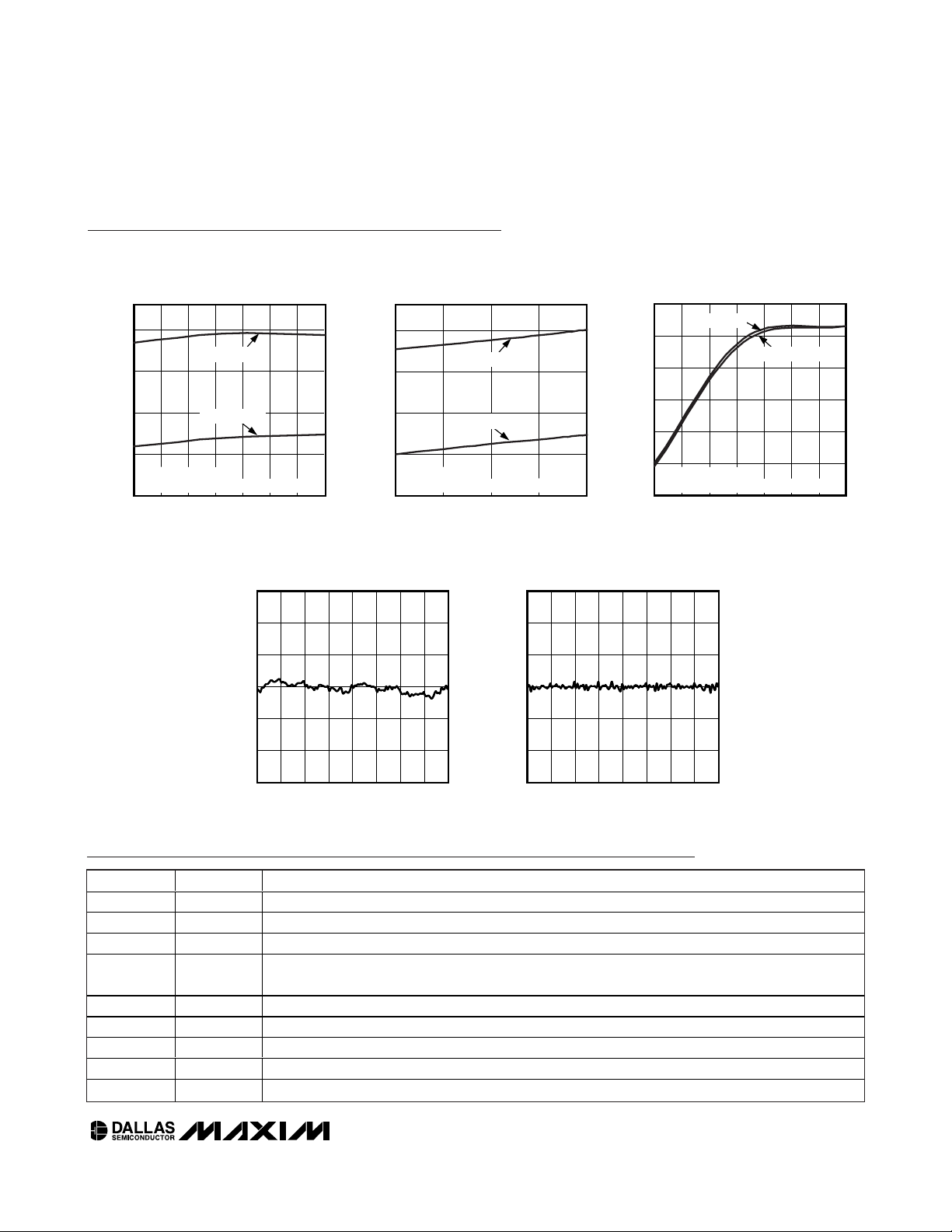
Typical Operating Characteristics
(TA = +25°C, unless otherwise noted.)
Typical Operating Characteristics
(TA = +25°C, unless otherwise noted.)
20
70
120
170
220
-40 0-20 20 40 60 80 100
SUPPLY CURRENT vs. TEMPERATURE
DS3501 toc01
TEMPERATURE (°C)
SUPPLY CURRENT (μA)
LUT MODE
DEFAULT MODE
V+ = 15.5V, VCC = 5V
SDA = SCL = V
CC
; RH, RL, RW ARE FLOATING
20
70
170
120
220
SUPPLY CURRENT vs. SUPPLY VOLTAGE
DS3501 toc02
SUPPLY VOLTAGE (V)
SUPPLY CURRENT (μA)
2.7 4.1 5.5
LUT MODE
DEFAULT MODE
V+ = 15.5V
SDA = SCL = V
CC
; RL, RH, RW ARE FLOATING
30
32
31
34
33
35
36
-40 20 40-20 0 60 80 100
STANDBY SUPPLY CURRENT
vs. TEMPERATURE
DS3501 toc03
TEMPERATURE (°C)
STANDBY SUPPLY CURRENT (μA)
LUT MODE
DEFAULT MODE
V+ = 15.5V, VCC = 5V
SDA = SCL = V
CC
; RH, RL, RW ARE FLOATING
-0.75
-0.50
-0.25
0
0.25
0.50
0.75
03216 48 64 80 96 112
INTEGRAL NONLINEARITY
vs. POTENTIOMETER SETTING
DS3501 toc04
POTENTIOMETER SETTING (DEC)
INTEGRAL NONLINEARITY (LSB)
-0.75
-0.50
-0.25
0
0.25
0.50
0.75
03216 48 64 80 96 112
DIFFERENTIAL NONLINEARITY
vs. POTENTIOMETER SETTING
DS3501 toc05
POTENTIOMETER SETTING (DEC)
DIFFERENTIAL NONLINEARITY (LSB)
Pin Description
NAME PIN DESCRIPTION
SDA 1 I2C Serial Data. Input/output for I2C data.
GND 2 Ground Terminal
V
CC
3 Supply Voltage Terminal
A1, A0 4, 5
Address Select Inputs. Determines I
2
C slave address. Slave address is 01010A1A0X. (See the Slave
Address Byte and Address Pins section for details).
RH 6 High Terminal of Potentiometer
RW 7 Wiper Terminal of Potentiometer
RL 8 Low Terminal of Potentiometer
V+ 9 Wiper Bias Voltage
SCL 10 I2C Serial Clock. Input for I2C clock.
Page 6

DS3501
High-Voltage, NV, I2C POT with Temp Sensor
and Lookup Table
6 _____________________________________________________________________
Default Mode Block Diagram (Update Mode bit = 0)
I2C
INTERFACE
LUT
ADDRESS
REGISTER
CONTROL
LOGIC/
REGISTERS
ADC
V
CC
SDA
A0
A1
GND
SCL
TEMP
SENSOR
V
CC
VOLTAGE
TEMP
0Ch
VCC (V)
0Eh
DATA
CONTROL
RH
RL
V+
POS 7Fh
POS 00h
RW
(LUTAR)
08h
36 BYTE
LOOKUP
TABLE
(LUT)
80h-A3h
WIPER
REGISTER
(WR)
09h*
INITIAL VALUE REGISTER
(IVR)
00h*
∑
ON POWER-UP
ONLY WHEN IN
LUT-ADDER MODE
IVR
LUTVAL OR
LUTVAL+IVR
LUTVAL
*NOTE THAT WHEN IN LUT OR LUT ADDER MODE, WR IS ACCESSED THROUGH 09h (UNLIKE DEFAULT MODE) WHILE IVR REMAINS AT 00h.
DS3501
LUT and LUT Adder Mode Block Diagram (Update Mode bit = 1)
Block Diagrams
V
CC
GND
SDA
SCL
I2C
INTERFACE
A0
A1
CONTROL
LOGIC/
REGISTERS
SEE BIT
DS3501
WIPER
REGISTER/
INITIAL VALUE
REGISTER
(WR/IVR)
00h
V+
RH
POS 7Fh
RW
POS 00h
RL
Page 7

DS3501
High-Voltage, NV, I2C POT with Temp Sensor
and Lookup Table
_____________________________________________________________________ 7
Detailed Description
The DS3501 operates in one of three operating modes:
Default Mode, LUT Mode, or LUT Adder Mode. In
Default Mode, the DS3501 is pin and software compatible with the ISL95311. The potentiometer’s wiper position is controlled by the Wiper Register (WR) and the
NV Initial Value Register (IVR) via the I
2
C interface. In
LUT Mode and LUT Adder Mode, the potentiometer’s
wiper position is calculated/controlled as a function of
the current temperature measured by the DS3501’s
internal temperature sensor. The difference between
the two LUT modes is the way the potentiometer wiper
position is calculated. A detailed description of the
three modes as well as additional features of the
DS3501 follow below.
Digital Potentiometer Output
The potentiometer consists of 127 resistors in series
connected between the RH and RL pins. Between each
resistance and at the two end points, RH and RL, solidstate switches enable RW to be connected within the
resistive network. The wiper position and the output on
RW are decoded based on the value in WR. If RH, RL,
and RW are externally connected in a voltage-divider
configuration, then the voltage on RW can be easily
calculated using the following equation:
where WR is the wiper position in decimal (0–127).
Temperature Conversion and
Supply Voltage Monitoring
Temperature Conversion
The DS3501 features an internal 8-bit temperature sensor that is capable of driving the LUT and providing a
measurement of the ambient temperature over I2C by
reading address 0Ch. The sensor is functional over the
entire operating temperature range and is in signed
two’s complement format with a resolution of 1°C/bit.
See below for the temperature sensor’s bit weights.
To calculate the temperature, treat the two’s complement binary value as an unsigned binary number, then
convert it to decimal. If the result is greater than or
equal to 128, subtract 256 from the result.
Supply Voltage Monitoring
The DS3501 also features an internal 8-bit supply voltage (VCC) monitor. A value of the supply voltage measurement can be read over I2C at the address 0Eh.
To calculate the supply voltage, simply convert the
hexadecimal result into decimal and then multiply it by
the LSB as shown in the
Analog Voltage Monitoring
Characteristics
electrical table.
Mode Selection
The DS3501 mode of operation is determined by two
bits located in Control Register 1 (CR1), which is nonvolatile. In particular, the mode is determined by the
Update Mode bit (CR1.0) and the Adder Mode bit
(CR1.1). Table 1 illustrates how the two control bits are
used to select the operating mode. When shipped from
the factory, the DS3501 is programmed with the CR1.0
bit = 0, hence configuring the DS3501 in Default Mode.
Default Mode
Default Mode of the DS3501 is the simplest mode of the
three. As shown in the Default Mode Block Diagram,
the potentiometer is controlled by the Wiper Register/
Initial Value Register (WR/IVR). Upon power-up of the
DS3501, the value stored in the NV Initial Value
Register (IVR) is recalled into the volatile Wiper
Register (WR). The wiper can then be changed any
time after by writing the desired value to the WR/IVR
Register. The WR/IVR Register is located at memory
address 00h and is implemented as EEPROM shadowed SRAM. This register can be visualized as an
SRAM byte (the WR portion) in parallel with a EEPROM
byte (the IVR portion). The operation of the register is
controlled by the Shadow EEPROM (SEE) bit, CR0.7.
When the SEE bit = 0 (default), data written to memory
address 00h by I2C actually gets stored in both SRAM
(WR) and EEPROM (IVR). Conversely, when SEE = 1,
only the SRAM (WR) is written to the new value. The
EEPROM byte (IVR) continues to store the last value
written to it when SEE was 0. Reading memory address
00h reads the value stored in WR. As shown in the
Default Mode memory map (see Table 2), the SEE bit is
volatile and its power-up default state is 0.
Table 1. DS3501 Operating Modes
VVWRVV
=+ −
RW RL RH RL
()
127
S262
4
2
3
2
5
2
2
1
2
0
2
UPDATE MODE
BIT (CR1.0)
0 X Default Mode (default)
1 0 LUT Mode
1 1 LUT Adder Mode
ADDER MODE
BIT (CR1.1)
MODE
Page 8

DS3501
High-Voltage, NV, I2C POT with Temp Sensor
and Lookup Table
8 _____________________________________________________________________
LUT Mode
LUT Mode is selected by setting the Update Mode bit
(CR1.0) to 1 and the Adder Mode bit (CR1.1) to 0. An
overview of the DS3501 in this mode is illustrated in the
LUT Mode and LUT Adder Mode Block Diagram. Also,
the memory map for LUT Mode and LUT Adder Mode is
shown in Table 3. The major difference between the two
LUT modes is whether or not the value in the IVR is
added to the values stored in the lookup table. The
dashed line/arrow shown in the block diagram is not
active in LUT mode.
When in LUT Mode, on power-up the IVR value is
recalled into the WR register. This value will remain
there until completion of the first temperature conversion following power-up. The temperature is measured
every t
FRAME
. The temperature value is used to calculate an index that points to the corresponding value in
the lookup table. This index is referred to as the LUT
Address Register (LUTAR). The value stored in the LUT
at the location pointed to by LUTAR is called LUTVAL.
The Wiper Register is then automatically loaded with
LUTVAL. The process then repeats itself, continuously
updating the wiper setting in a closed-loop fashion.
In this mode the 36-byte LUT is populated with wiper
settings for each four-degree temperature window.
Valid wiper settings are 00h to 7Fh. The memory map in
Table 3 shows the memory address of the LUT as well
as the corresponding temperature range for each byte
in the LUT. Also, the LUT features one-degree hysteresis to prevent chattering if the measured temperature
Table 2. Default Mode Memory Map
*
In Default Mode, both WR and IVR are accessed through memory location 00h. Refer to the Default Mode section for additional information.
Table 3. LUT Mode and LUT Adder Mode Memory Map
*
In LUT Mode and LUT Adder Mode, the WR is accessed through memory address 09h, while IVR remains at memory address 00h.
REGISTER NAME
WR/IVR
CR0 Control Register 0 02h V 00h
CR1 Control Register 1 03h NV (Shadowed) 00h
CR2 Control Register 2 0Ah V 00h
Wiper Register/Initial Value
ADDRESS
(HEX)
00h* NV (Shadowed) 40h
VOLATILE/NONVOLATILE
REGISTER NAME
IVR Initial Value Register 00h* NV (Shadowed) 40h
CR0 Control Register 0 02h V 00h
CR1 Control Register 1 03h NV (Shadowed) 00h
LUTAR LUT Address Register 08h V N/A
WR Wiper Register 09h* V N/A
CR2 Control Register 2 0Ah V 00h
TEMP Temperature Value 0Ch V (Read-Only) N/A
VCC VCC Voltage Value 0Eh V (Read-Only) N/A
LUT0 Wiper Value for T ≤ -37°C 80h NV 00h
LUT1 Wiper Value for -36°C to -33°C 81h NV 00h
LUT2 Wiper Value for -32°C to -29°C 82h NV 00h
———— —
LUT33 Wiper Value for +92°C to +95°C A1h NV 00h
LUT34 Wiper Value for +96°C to +99°C A2h NV 00h
LUT35 Wiper Value for T ≥ 100°C A3h NV 00h
ADDRESS
(HEX)
VOLATILE/NONVOLATILE
FACTORY/POWER-UP
DEFAULT
FACTORY/POWER-UP
DEFAULT
Page 9

DS3501
High-Voltage, NV, I2C POT with Temp Sensor
and Lookup Table
_____________________________________________________________________ 9
falls on the boundary between two windows. As the
temperature increases, the LUT changes on even temperature values (see Figure 1). Conversely, the LUT
changes on odd temperature values when the temperature is decreasing.
LUT Adder Mode
LUT Adder Mode is selected by setting the Update
Mode bit (CR1.0) to 1 and the Adder Mode bit (CR1.1)
to 1. This mode operates similar to LUT Mode with one
major difference (see the LUT Mode and LUT Adder
Mode Block Diagram). The Wiper Register is loaded
with the sum of LUTVAL and IVR. Furthermore, in this
mode, the values programmed into the LUT are signed
two’s complement. This allows convenient positive or
negative offsetting of the nominal IVR value.
Figure 1. LUT Hysteresis
DS3501 Control Registers
The DS3501 contains three control registers (CR0, CR1, and CR2) used to configure and control modes and features.
LUT20
LUT19
DECREASING
TEMPERATURE
LUT18
MEMORY LOCATION
LUT17
LUT16
24 28 32 36 40 44
1°C HYSTERESIS
TEMPERATURE (°C)
WINDOW
INCREASING
TEMPERATURE
Control Register 0 (CR0)
POWER-UP DEFAULT 00h
MEMORY TYPE Volatile
02h
SEE
bit7 bit0
Reserved Reserved Reserved Reserved Reserved Reserved Reserved
bit7
bit6:0 Reserved
Control Register 1 (CR1)
FACTORY DEFAULT 00h
MEMORY TYPE Shadowed Nonvolatile
bit7:2 Reserved
bit1
bit0
SEE: Controls functionality of shadowed NV registers (such as the WR/IVR register).
0 = Data written to shadowed NV memory is stored in both SRAM and EEPROM (default).
1 = Data written to shadowed NV memory is stored only in SRAM.
03h
Reserved Reserved Reserved Reserved Reserved Reserved
bit7 bit0
Adder Mode: This bit is valid only if the Update Mode bit = 1.
0 = Sets the DS3501 to LUT Mode.
1 = Sets the DS3501 to LUT Adder Mode.
Update Mode:
0 = Sets the DS3501 to Default Mode. In this mode the DS3501 is compatible with the ISL95311 (default).
1 = Sets the DS3501 to one of the two LUT-based modes depending on the Adder Mode bit.
Adder
Mode
Update
Mode
Page 10

DS3501
High-Voltage, NV, I2C POT with Temp Sensor
and Lookup Table
10 ____________________________________________________________________
Standby Mode and I
CC
The DS3501 has three specified levels of supply current. Active current during I2C communications while in
the LUT-driven mode is specified as ICC, and is the
“worst-case” supply current. Active current without I2C
communications while in the LUT driven mode is specified as the supply current: I
CC2
. SDA and SCL are held
statically in the high-logic level while the DS3501 continues to function in LUT-driven mode. The third level is
specified as standby mode, I
STBY
. This is the lowest
possible current consumption mode.
Standby mode is enabled with CR2.0 = 1. All internal
operations are halted including internal temperature
sensor results. Consequently, WR’s position will not
change, and will remain in the last state that was
loaded into WR. I2C will, however, continue to function,
and once CR2.0 = 0, the DS3501 will resume normal
operation after the first temperature conversion cycle is
complete (t
FRAME
).
Slave Address Byte and Address Pins
The slave address byte consists of a 7-bit slave
address plus a R/W bit (see Figure 2). The DS3501’s
slave address is determined by the state of the A0 and
A1 address pins. These pins allow up to four devices to
reside on the same I2C bus. Address pins tied to GND
result in a 0 in the corresponding bit position in the
slave address. Conversely, address pins tied to V
CC
result in a 1 in the corresponding bit positions. For
example, the DS3501’s slave address byte is 50h when
A0 and A1 pins are grounded. I2C communication is
described in detail in the
I2C Serial Interface
Description
section.
I2C Serial Interface Description
I2C Definitions
The following terminology is commonly used to describe
I
2
C data transfers. (See Figure 3 and
I2C AC Electrical
Characteristics
table for additional information.)
Master device: The master device controls the slave
devices on the bus. The master device generates SCL
clock pulses and START and STOP conditions.
Figure 2. DS3501 Slave Address Byte
Control Register 2 (CR2)
POWER-UP DEFAULT 00h
MEMORY TYPE Volatile
0Ah Reserved Reserved Reserved Reserved Reserved
bit7:3 Reserved
bit2
bit1
bit0
bit7 bit0
TEN: Temperature Update Enable bar. This bit is valid only in LUT Mode and LUT Adder Mode.
0 = Normal LUT operation. The WR is automatically loaded with LUTVAL+IVR or LUTVAL following each
temperature conversion.
1 = Places the potentiometer in manual mode allowing WR (09h) to be written using I
AEN: Address Update Enable bar. This bit is valid only in LUT Mode and LUT Adder Mode.
0 = Normal LUT operation. LUTAR (08h) is calculated following each temperature conversion that points to the
corresponding location in the LUT.
1 = Disables automatic updates of LUTAR. This allow the user to directly write to the LUTAR register in order to
exercise LUT values and functionality.
Standby:
0 = Normal operating mode.
1 = Standby Mode. Places the DS3501 in a low-power consumption state specified by I
is still active in this state.
TEN AEN
2
C.
MSB
0
1
*THE SLAVE ADDRESS IS DETERMINED BY ADDRESS PINS A0, A1.
1
0
SLAVE ADDRESS*
. The I2C interface
STBY
0
A1
Standby
LSB
R/W
A0
Page 11

DS3501
High-Voltage, NV, I2C POT with Temp Sensor
and Lookup Table
____________________________________________________________________ 11
Slave devices: Slave devices send and receive data at
the master’s request.
Bus idle or not busy: Time between STOP and START
conditions when both SDA and SCL are inactive and in
their logic-high states.
START condition: A START condition is generated by
the master to initiate a new data transfer with a slave.
Transitioning SDA from high to low while SCL remains
high generates a START condition.
STOP condition: A STOP condition is generated by the
master to end a data transfer with a slave. Transitioning
SDA from low to high while SCL remains high generates
a STOP condition.
Repeated START condition: The master can use a
repeated START condition at the end of one data transfer
to indicate that it will immediately initiate a new data
transfer following the current one. Repeated starts are
commonly used during read operations to identify a specific memory address to begin a data transfer. A repeated START condition is issued identically to a normal
START condition.
Bit write: Transitions of SDA must occur during the low
state of SCL. The data on SDA must remain valid and
unchanged during the entire high pulse of SCL plus the
setup and hold time requirements. Data is shifted into the
device during the rising edge of the SCL.
Bit read: At the end of a write operation, the master
must release the SDA bus line for the proper amount of
setup time before the next rising edge of SCL during a
bit read. The device shifts out each bit of data on SDA
at the falling edge of the previous SCL pulse and the
data bit is valid at the rising edge of the current SCL
pulse. Remember that the master generates all SCL
clock pulses, including when it is reading bits from the
slave.
Acknowledge (ACK and NACK): An Acknowledge
(ACK) or Not Acknowledge (NACK) is always the 9th bit
transmitted during a byte transfer. The device receiving
data (the master during a read or the slave during a
write operation) performs an ACK by transmitting a 0
during the 9th bit. A device performs a NACK by transmitting a 1 during the 9th bit. Timing for the ACK and
NACK is identical to all other bit writes. An ACK is the
acknowledgment that the device is properly receiving
data. A NACK is used to terminate a read sequence or
indicates that the device is not receiving data.
Byte write: A byte write consists of 8 bits of information
transferred from the master to the slave (most significant bit first) plus a 1-bit acknowledgment from the
slave to the master. The 8 bits transmitted by the master are done according to the bit write definition and the
acknowledgment is read using the bit read definition.
Byte read: A byte read is an 8-bit information transfer
from the slave to the master plus a 1-bit ACK or NACK
from the master to the slave. The 8 bits of information
that are transferred (most significant bit first) from the
slave to the master are read by the master using the bit
read definition above, and the master transmits an ACK
using the bit write definition to receive additional data
bytes. The master must NACK the last byte read to ter-
Figure 3. I2C Timing Diagram
SDA
t
SCL
STOP
BUF
START
t
LOW
t
HD:STA
t
R
t
HD:DAT
t
HD:STA
t
F
t
t
HIGH
t
SU:DAT
REPEATED
START
SU:STA
t
SP
t
SU:STO
NOTE: TIMING IS REFERENCE TO V
IL(MAX)
AND V
IH(MIN)
.
Page 12

DS3501
High-Voltage, NV, I2C POT with Temp Sensor
and Lookup Table
12 ____________________________________________________________________
minate communication so the slave will return control of
SDA to the master.
Slave address byte: Each slave on the I2C bus
responds to a slave address byte sent immediately following a START condition. The slave address byte contains the slave address in the most significant 7 bits
and the R/W bit in the least significant bit. The slave
address byte of the DS3501 is shown in Figure 2.
When the R/W bit is 0 (such as in 50h), the master is
indicating it will write data to the slave. If R/W = 1 (51h
in this case), the master is indicating it wants to read
from the slave.
If an incorrect slave address is written, the DS3501
assumes the master is communicating with another I2C
device and ignores the communication until the next
START condition is sent.
Memory address: During an I2C write operation, the
master must transmit a memory address to identify the
memory location where the slave is to store the data.
The memory address is always the second byte transmitted during a write operation following the slave
address byte.
I2C Communication
Writing a single byte to a slave: The master must generate a START condition, write the slave address byte
(R/W = 0), write the memory address, write the byte of
data, and generate a STOP condition. Remember the
master must read the slave’s acknowledgment during
all byte write operations.
When writing to the DS3501, the potentiometer will adjust
to the new setting once it has acknowledged the new
data that is being written, and the EEPROM (if SEE = 0)
will be written following the STOP condition at the end of
the write command. To change the setting without
changing the EEPROM, terminate the write with a repeated START condition before the next STOP condition
occurs. Using a repeated START condition prevents the
tWdelay required for the EEPROM write cycle to finish.
Writing multiple bytes to a slave: To write multiple
bytes to a slave in one transaction, the master generates a START condition, writes the slave address byte
(R/W = 0), writes the memory address, writes up to 8
data bytes, and generates a STOP condition. The
DS3501 is capable of writing 1 to 8 bytes (1 page or
row) in a single write transaction. This is internally controlled by an address counter that allows data to be
written to consecutive addresses without transmitting a
memory address before each data byte is sent. The
address counter limits the write to one 8-byte page
(one row of the memory map). The first page begins at
address 00h and subsequent pages begin at multiples
of 8 (08h, 10h, 18h, etc). Attempts to write to additional
pages of memory without sending a STOP condition
between pages results in the address counter wrapping around to the beginning of the present row. To
prevent address wrapping from occurring, the master
must send a STOP condition at the end of the page,
then wait for the bus-free or EEPROM-write time to
elapse. Then the master can generate a new START
condition and write the slave address byte (R/W = 0)
and the first memory address of the next memory row
before continuing to write data.
Acknowledge polling: Any time a EEPROM byte is
written, the DS3501 requires the EEPROM write time
(tW) after the STOP condition to write the contents of
the byte to EEPROM. During the EEPROM write time,
the device will not acknowledge its slave address
because it is busy. It is possible to take advantage of
this phenomenon by repeatedly addressing the
DS3501, which allows communication to continue as
soon as the DS3501 is ready. The alternative to
acknowledge polling is to wait for a maximum period of
tWto elapse before attempting to access the device.
EEPROM write cycles: The DS3501’s EEPROM write
cycles are specified in the
Nonvolatile Memory
Characteristics
table. The specification shown is at the
worst-case temperature (hot) as well as at room temperature. Writing to shadowed EEPROM with SEE = 1
does not count as a EEPROM write.
Reading a single byte from a slave: Unlike the write
operation that uses the specified memory address byte
to define where the data is to be written, the read operation occurs at the present value of the memory address
counter. To read a single byte from the slave, the master
generates a START condition, writes the slave address
byte with R/W = 1, reads the data byte with a NACK to
indicate the end of the transfer, and generates a STOP
condition. However, since requiring the master to keep
track of the memory address counter is impractical, the
following method should be used to perform reads from
a specified memory location.
Manipulating the address counter for reads: A
dummy write cycle can be used to force the address
counter to a particular value. To do this the master generates a START condition, writes the slave address
byte (R/W = 0), writes the memory address where it
desires to read, generates a repeated START condition, writes the slave address byte (R/W = 1), reads
data with ACK or NACK as applicable, and generates a
STOP condition.
See Figure 4 for a read example using the repeated
START condition to specify the starting memory location.
Page 13

DS3501
High-Voltage, NV, I2C POT with Temp Sensor
and Lookup Table
____________________________________________________________________ 13
Reading multiple bytes from a slave: The read opera-
tion can be used to read multiple bytes with a single
transfer. When reading bytes from the slave, the master
simply ACKs the data byte if it desires to read another
byte before terminating the transaction. After the master
reads the last byte it must NACK to indicate the end of
the transfer and generates a STOP condition.
Applications Information
Power-Supply Decoupling
To achieve the best results when using the DS3501,
decouple both the power-supply pin and the wiper-bias
voltage pin with a 0.01µF or 0.1µF capacitor. Use a
high-quality ceramic surface-mount capacitor if possible. Surface-mount components minimize lead inductance, which improves performance, and ceramic
capacitors tend to have adequate high-frequency
response for decoupling applications.
SDA and SCL Pullup Resistors
SDA is an I/O with an open-collector output that
requires a pullup resistor to realize high-logic levels. A
master using either an open-collector output with a
pullup resistor or a push-pull output driver can be used
for SCL. Pullup resistor values should be chosen to
ensure that the rise and fall times listed in the
I2C AC
Electrical Characteristics
are within specification. A typ-
ical value for the pullup resistors is 4.7kΩ.
Chip Information
TRANSISTOR COUNT: 22,400
SUBSTRATE CONNECTED TO GROUND
Figure 4. I2C Communication Examples
2
C WRITE TRANSACTION
TYPICAL I
MSB LSB MSB LSB MSB LSB
START
0 1 0 1 0 A1 A0 R/W
SLAVE
ADDRESS*
2
C TRANSACTIONS (WHEN A0 AND A1 ARE CONNECTED TO GND).
EXAMPLE I
A)
SINGLE-BYTE WRITE
-WRITE LUTAR
REGISTER TO 00h
B)
SINGLE-BYTE READ
-READ CR0 REGISTER
C)
SINGLE-BYTE WRITE
SET TO LUT MODE
D)
TWO-BYTE WRITE
- WRITE 80h AND 81h TO 00h
TWO-BYTE READ
E)
- READ 80h AND 81H
0 1010000
START
0 1010000
START
0 1010000 00000011
START
0 1010000 10000000
START
0 1010000 10000000
START
SLAVE
b7 b6 b5 b4 b3 b2 b1 b0
ACK
READ/
WRITE
50h 08h
SLAVE
00001 000
ACK
50h
SLAVE
50h CR1 (03h)
SLAVE
50h 80h
SLAVE
50h 80h
SLAVE
ACK
ACK
ACK
ACK
02h
00000 010
SLAVE
b7 b6 b5 b4 b3 b2 b1 b0
ACK
REGISTER ADDRESS
*THE SLAVE ADDRESS IS DETERMINED BY ADDRESS PINS A0 AND A1.
SLAVE
ACK
SLAVE
ACK
SLAVE
ACK
SLAVE
ACK
SLAVE
ACK
00000 000
REPEATED
START
000 0 0 01
0
000 0 0 00
0
REPEATED
START
01h
00h
SLAVE
ACK
51h
01010 001
SLAVE
ACK
SLAVE
ACK
51h
101 0 0 01
0
STOP
SLAVE
ACK
STOP
00h
000 0 0 00
0
SLAVE
ACK
DATA
SLAVE
ACK
DATA
DATA
MASTER
STOP
NACK
MASTER
ACK
STOP
DATA
LUT 1LUT 0
SLAVE
ACK
STOP
MASTER
ACK
STOP
Page 14

V
CC
2.7V
GND
RL
RW
V+
RH
SCL
I
2
C
C
LCD
V
COM
R1
G1
B1
GATE 1
GATE 2
GATE 3
C
STOR
TFT
A1
A0
15.0V
SDA
DS3501
Typical Operating Circuit
10
9
8
7
6
1
2
3
4
5
SCL
V+
RL
RWA1
V
CC
GND
SDA
TOP VIEW
RHA0
DS3501
Pin Configuration
Package Information
For the latest package outline information, go to
www.maxim-ic.com/DallasPackInfo
.
DS3501
High-Voltage, NV, I2C POT with Temp Sensor
and Lookup Table
Maxim cannot assume responsibility for use of any circuitry other than circuitry entirely embodied in a Maxim product. No circuit patent licenses are
implied. Maxim reserves the right to change the circuitry and specifications without notice at any time.
14
____________________Maxim Integrated Products, 120 San Gabriel Drive, Sunnyvale, CA 94086 408-737-7600
© 2007 Maxim Integrated Products is a registered trademark of Maxim Integrated Products, Inc.
is a registered trademark of Dallas Semiconductor Corporation.
Heaney
 Loading...