

Page 1
Y
K
K
STS
t
STS
www.maxim-ic.com
FEATURES
Integrated transmit and receive for T3, E3,
and STS-1 line interfaces
Performs clock/data recovery and wave
shaping
Requires no special external components
other than 1:2 transformers
Interfaces to 75Ω coaxial cable at lengths up
to 380m (T3), 440m (E3), or 360m (STS-1)
Adaptive receive equalizer handles from 0dB
to 15dB of cable loss
Interfaces directly to a DSX monitor signal
(20dB flat loss)
On-chip jitter attenuator can be placed either
in the receive path or the transmit path
Built-in B3ZS and HDB3 coder/decoder
Bipolar and NRZ interfaces
Analog and digital loopbacks
Onboard 215 - 1 and 223 - 1 Pseudo Random
Bit Sequence (PRBS) generator and detector
Transmit line-driver monitor checks for a
faulty transmitter or a shorted output
Complete T3 AIS generator (ANSI T1.107)
Unframed all ones generator (E3 AIS)
Digital clock inversion capability
Three-state line driver for low-power mode
Loss-of-signal detector (ANSI T1.231-1999
and ITU G.775)
Pin compatible with the TDK 78P7200 and
78P7200L
Drop-in replacement for TDK 78P2241/B
(Refer to Application Note 362)
Low-power 3.3V operation (5V tolerant I/O)
Industrial temperature range: -40°C to +85°C
Small packaging: 28-pin PLCC and
48-pin TQFP
PRELIMINARY
PRELIMINAR
DS3150
3.3V T3/E3/STS-1 Line Interface Unit
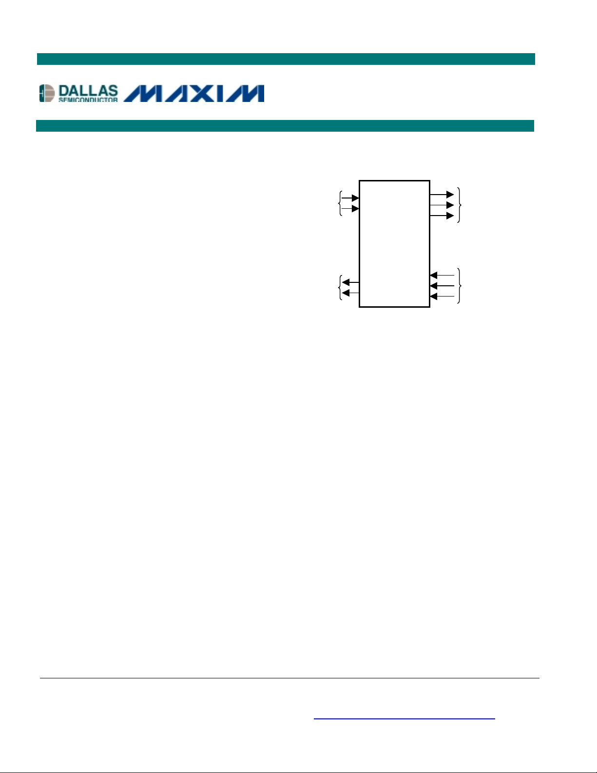
FUNCTIONAL DIAGRAM
Line In
T3, E3,
-1
Rx+
Rx-
Line Ou
T3, E3,
-1
Tx+
Tx-
DS3150 LIU
ORDERING INFORMATION
DS3150QN 28-Pin PLCC -40°C to +85°C
DS3150Q 28-Pin PLCC 0°C to +70°C
DS3150TN 48-Pin TQFP -40°C to +85°C
DS3150T 48-Pin TQFP 0°C to +70°C
RCL
RPOS
RNE
TCL
TPOS
TNEG
Receive
Clock and
Data
Transmit
Clock and
Data
Note: Some revisions of this device may incorporate deviations from published specifications known
as errata. Multiple revisions of any device may be simultaneously available through various sales
channels. For information about device errata, click here: http://dbserv.maxim-ic.com/errata.cfm
1 of 22 020602
.
Page 2

TABLE OF CONTENTS
1. FUNCTIONAL DESCRIPTION ……………………………………………………………..3
2. SIGNAL DESCRIPTION……………………………………………………………………13
3. AC CHARACTERISTICS …………………………...………………...……………………17
4. PIN ASSIGNMENTS ………………………………………………………………………19
5. MECHANICAL DIMENSIONS ………………...……………...…………………………..20
6. APPLICATIONS……………..……………………………………………………….……..22
DS3150
2 of 22
Page 3
DS3150
r
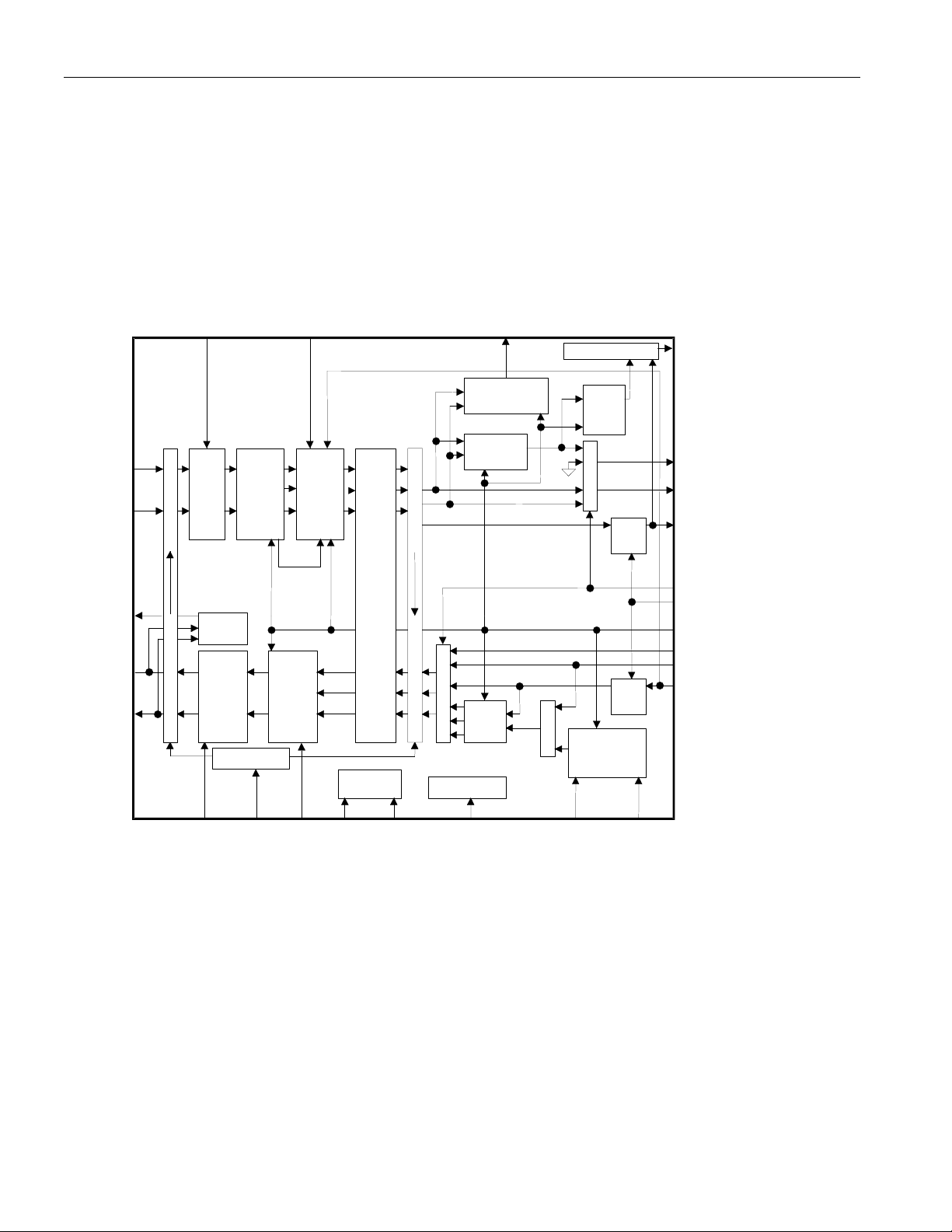
1. FUNCTIONAL DESCRIPTION
The DS3150 performs all the functions necessary for interfacing at the physical layer to T3, E3, and STS1 lines. The device has independent receive and transmit paths (Figure 1A). The receiver performs clock
and data recovery from a B3ZS-code or HDB3-code AMI signal and monitors for loss of the incoming
signal. The recovered data optionally can be B3ZS/HDB3 decoded and output in NRZ format. The
transmitter accepts either NRZ or bipolar data and drives standard pulse-shape waveforms onto 75!
coaxial cable. The receiver and transmitter sections will be discussed separately below. Table 1A lists the
telecommunications standards that the DS3150 was designed to meet.
Figure 1A. DS3150 BLOCK DIAGRAM
RX+
RX-
DM*
TX+
TX-
liu_bd
RMON
20dB
Flat
Gain
Analog
Loopback
Driver
Monitor
Line
Driver
Loopback Control
Filter/
Equalizer
(Analog
Loss Of
Signal
Detect)
Squelch
WaveShaping
Clock &
Data
Recovery
Jitter Attenuato
Power
Connections
LOS*MCLK
Output Decode
Digital Loss Of
Signal Detector
B3ZS/HDB3
Decoder
Remote
Loopback
Mux
(can be placed in either the receive path or the transmit path)
B3ZS/
HDB3
Encoder
Test Functions
Mux
PRBS
Detector
mux
AIS/
1010.../
PRBS
Generation
Clock
Invert
Clock
Invert
PRBS
RPOS/RNRZ
RNEG/RLCV
RCLK
ZCSE*
ICE
TESS
TNEG
TPOS/TNRZ
TCLK
TTS*
LBKS*
3 of 22
LBO
V
DD
SS
EFEV
TDS0 TDS1
Page 4
DS3150
Table 1A. APPLICABLE STANDARDS
T1.102-1993 (ANSI) “Digital Hierarchy–Electrical Interfaces”
T1.107-1995 (ANSI) “Digital Hierarchy–Formats Specification”
T1.231-1997 (ANSI) Draft “Digital Hierarchy–Layer 1 In-Service Digital Transmission
Performance Monitoring”
T1.231-1993 (ANSI) “Digital Hierarchy–Layer 1 In-Service Digital Transmission Performance
Monitoring”
T1.404-1994 (ANSI) “Network-to-Customer Installation–DS3 Metallic Interface Specification”
GR-499-CORE (Bellcore) Issue 1, December 1995 “Transport Systems Generic Requirements
(TSGR): Common Requirements”
GR-253-CORE (Bellcore) Issue 2, December 1995 “SONET Transport Systems: Common Generic
Criteria”
G.703, 1991 (ITU) “Physical/Electrical Characteristics of Hierarchical Digital Interfaces
G.751, 1993 (ITU) “Digital Multiplex Equipment Operating at the Third Order Bit Rate of
34,368kbit(s) and the Fourth Order Bit Rate of 139,264kbit(s) and Using Postive
Justification”
G.823, 1993 (ITU) “The Control of Jitter and Wander Within Digital Networks that are based
on the 2048kbit(s) Hierarchy”
G.775, 1994 (ITU) “Loss of Signal (LOS) and Alarm Indication Signal (AIS) Defect Detection
and Clearance Criteria”
O.151, 1992 (ITU) “Error Performance Measuring Equipment Operating at the Primary Rate
and Above”
TBR 24, 1997 (ETSI) “Business TeleCommunications; 34Mbit(s) digital unstructured and
structured lease lines; attachment requirements for terminal equipment interface
ETS 300 687, 1996 (ETSI) “Business TeleCommunications; 34Mbit(s) digital leased lines (D34U and
D34S); Connection characteristics
ETS 300 686, 1996 (ETSI) “Business TeleCommunications; 34Mbit(s) and 140Mbits(s) digital leased
lines (D34U, D34S, D140U, and D140S); Network interface presentation
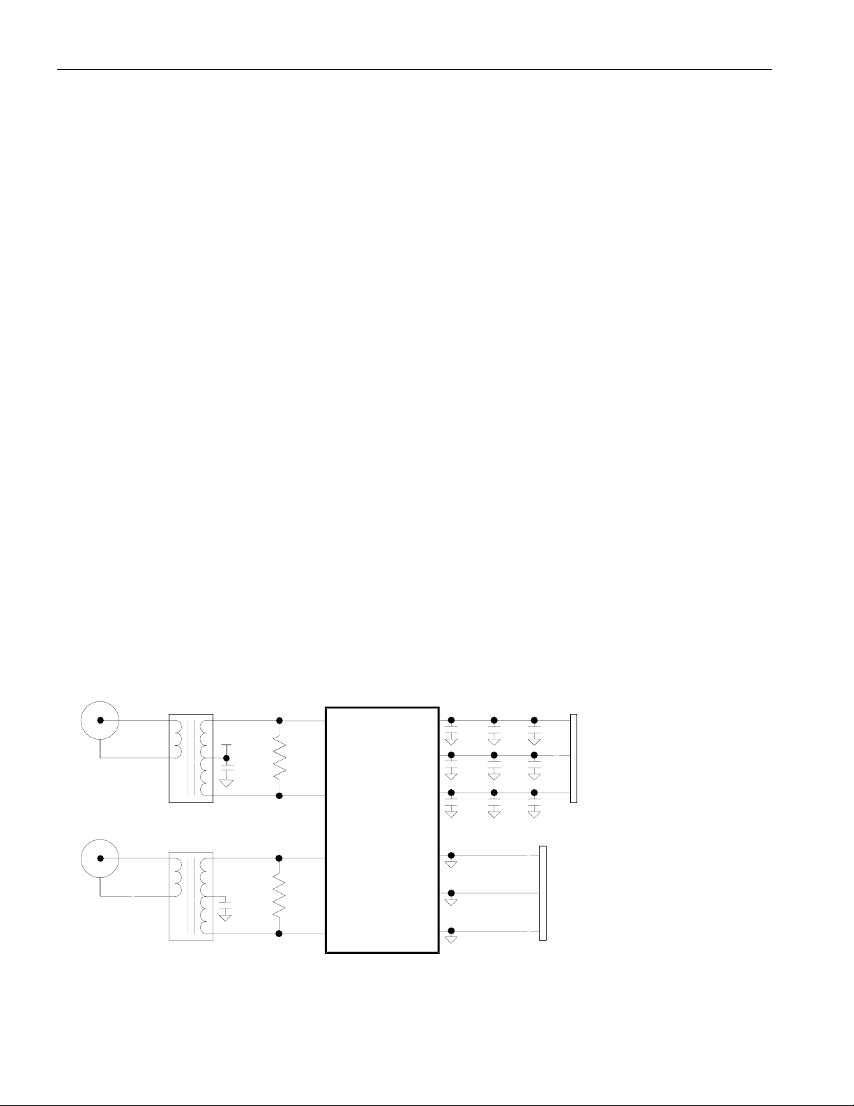
Figure 1B. EXTERNAL CONNECTION
Transmit
V
Receive
1:2ct
1:2ct
VDD
0.05µF
0.05µF
330Ω
(1%)
330Ω
(1%)
TX+
TX-
DS3150
RX+
RX-
DD
V
DD
0.01µF
0.01µF
0.1µF
0.1µF
1µF
1µF
3.3V
Power
Plane
V
DD
V
SS
V
SS
0.01µF
0.1µF
1µF
Ground
Plane
V
SS
4 of 22
Page 5

DS3150
Table 1B. DS3150 T3/E3/STS-1 LIU TRANSFORMER RECOMMENDATIONS
MANUFACTURER
Pulse Engineering
Pulse Engineering
Halo Electronics
Halo Electronics
Note: Table subject to change. Commercial Temp: 0°C to +70°C
PART
NO.
PE-
65968
PE-
65969
TG07-
0206NS
TD07-
0206NE
TURNS
RATIO
1:2CT LS-1/C 6-pin SMT 19 0.06 0.250 to 500
1:2CT LC-1/C 6-pin thru-hole 19 0.06 0.250 to 500
1:2CT SMD/B 6-pin SMT 19 0.06 0.250 to 500
1:2CT DIP/B 6-pin DIP 19 0.06 0.250 to 500
PKG/
SCHEMATIC
DESCRIPTION
OCL
PRIMARY
µµµµH
BANDWIDTH
L
L
µµµµH
75ΩΩΩΩ (MHz)
RECEIVER
The DS3150 interfaces to the receive T3/E3/STS-1 coax line through a 1:2 step-up transformer
(Figure 1B). The receiver automaticall y adapts to coax cable loses from 0d B to 15dB, which translates
into 0m to 380m (T3) or 440m (E3) or 360m (STS-1) of coax cable (AT&T 734A or equivalent). The
receiver also has the ability to interface to monitor jacks. Through the RMON input (Table 2A), the
device can be configured to insert a 20dB flat boost into the incoming signal. Monitor jacks typically
have series resistors that result in a resistive loss of 20dB. The receiver has excellent jitter tolerance
characteristics (Figure 1C).
The receiver contains bot h analog and digital loss-of-signal (LOS) detect ors. The analog LOS detector
resides in the equalizer. If the incoming signal drops below -24dB of the nominal signal level, the a nalog
LOS detector will activate and it will step on the recovered data and force all zeros out of the data
recovery circuitry. The analog LOS detector will not clear until the signal level is above
-18dB of the nominal signal level. The digital LOS detector is activated when it detects 192±1
consecutive zeros. LOS is clear ed when there are no excessive zero occurrences ove r a span of 192±1
clock periods. An excessive zero occurrence is defined as t hree or more consecutive zeros in the T3 and
STS-1 modes and four or more zeros in the E3 mode. The status of the digital LOS is reflected at the
LOS* output (Table 2A). There is no status output available for the analog LOS detector. While the
device is in a LOS state, the RCLK output will be referenced to the MCLK input (or the TC LK input if
MCLK is high/floating or to the internal oscillator if MCLK is tied low). The analog LOS detector has a
longer time constant than the digital LOS. Hence, when the incoming signal is lost, the digital LOS will
activate first followed by the analog LOS detector. When a signal is restored, the digital LOS will not be
allowed to qualify a signal for no excessive zero violations until the analog LOS detector has seen the
signal rise above -18dB. Governing specifications for the LOS detectors are ANSI T1.231 and ITU
G.775.
The recovered data from the receiver can be output in either bipolar format or nonreturn-to -zero (NRZ)
format. To select the bipolar format, the ZCSE* input is tied high. In this format, the B3ZS/HDB3
decoder is disabled and the received data is buffered and then output on the RPOS and RNEG outputs. To
select the NRZ format, the ZCSE* input is tied low. In this format, the B3ZS/HBD3 decoder is enabled
and the recovered data is B3ZS/HDB3 decoded and then logicall y OR’ed together at the RNRZ output,
while the RLCV output indicates line code violations.
5 of 22
Page 6
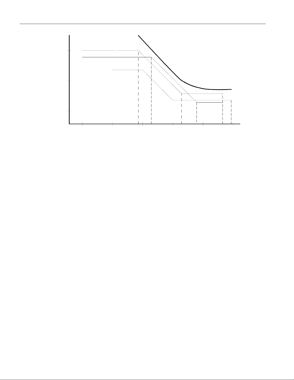
Figure 1C. RECEIVER JITTER TOLERANCE
J
(U
p
p
)
T3 [GR-499 (1995)]
10
l
1.0
Category II
T3 [GR-499 (1995)]
Category I
E3 [G.823(1993)]
10
5
1.5
DS3150
Jitter
Tolerance
DS3150
itter Tolerance
0.1
0.3
0.15
0.1
10 100 1k 10k 100k 1M
60k22.3k2.3k669
300k 800k
Frequency (Hz)
6 of 22
Page 7

DS3150
TRANSMITTER
Through the ZCSE* input, the device is configured to accept either bipolar data or NRZ data to be input
to the transmitter. When the ZCSE* input is tied high, bipolar data must be applied at the TPOS and
TNEG inputs. In this mode, the device will not perform B3ZS/HDB3-encoding on the outgoing data
stream. When the ZCSE* input is tied low, an NRZ data stream must be applied at the TPOS input
(TNEG is ignored). In this mode, the device will perform B3ZS/HDB3-encoding on the outgoing data
stream.
The clock applied at the TCLK input is used to transmit data onto the T3/E3/STS-1 line. Hence, TCLK
must be of transmission quality (i.e., accurate to ±20ppm). The duty cycle of TCLK is not a key
parameter as long as the clock high and low times listed in Section 3 are met.
The DS3150 also has the ability to generate a number of different patterns, including an unframed all
ones pattern, which is also the E3 AIS signal; a 101010… pattern; or a T3 Alarm Indication Signal (AIS).
See Figure 1E for a description of the T3 AIS. The TDS0 and TDS1 inputs are used to select these
onboard patterns (Tables 2A and 2B).
The DS3150 interfaces to the transmit T3/E3/STS-1 coax cable through a 1:2 step up transformer (Figure
1B). It will drive the 75! cable and create the proper waveforms required for interfacing to T3/E3/STS-1
lines. In T3 and STS-1 modes, the LBO (line build out) pin controls waveform shape. For cable lengths
fewer than 225ft, LBO should be pulled high. For 225ft or more of cable, LBO should be pulled low.
Tables 1C through 1G and Figure 1D detail the waveform template specifications and testing parameters.
The transmitter can be disabled and the Tx+ and Tx- outputs three-stated through the TTS* input (Table
2A).
The transmit driver monitor constantly checks the analog signal output at Tx+ and Tx-. If the output fails,
then the DM* output will be pulled low. When the transmitter is disabled (TTS* = 0), the driver monitor
is also disabled.
Table 1C. T3 TRANSMIT WAVEFORM TEMPLATE
TIME AXIS RANGE NORMALIZED AMPLITUDE EQUATIONS
Upper
Curve
-0.85 ≤ T ≤ -0.68
-0.68 ≤ T ≤ 0.36 0.5 {1 + sin[(π / 2)(1 + T / 0.34)]} + 0.03
0.36 ≤ T ≤ 1.4
Lower
Curve
-0.85 ≤ T ≤ -0.36
-0.36 ≤ T ≤ 0.36 0.5 {1 + sin[(π/2)(1 + T/0.18)]} - 0.03
0.36 ≤ T ≤ 1.4
Governing Specifications: ANSI T1.102-1993 and Bellcore GR-499
0.03
0.08 + 0.407e
-0.03
-0.03
-1.84(T - 0.36)
7 of 22
Page 8

DS3150
Table 1D. T3 TRANSMIT WAVEFORM TEST PARAMETERS AND LIMITS
PARAMETER SPECIFICATION
Rate
44.736Mbps (±20ppm)
Line Code B3ZS
Transmission Medium Coax cable (AT&T 734A or equivalent)
Test Measurement Point At the end of 0ft to 450ft of coax cable
Test Termination
75Ω (± 1%) resistive
Pulse Amplitude Between 0.36V and 0.85V
Pulse Shape An isolated pulse (preceded by two zeros and followed by
one or more zeros) falls within the curves listed in Table 1C
Unframed All Ones Power Level
Between -1.8dBm and +5.7dBm
at 22.368MHz
Unframed All Ones Power Level
At least 20dB less than the power measured at 22.368MHz
at 44.736MHz
Pulse Imbalance of Isolated Pulses Ratio of positive and negative pulses must be between 0.90
and 1.10
Table 1E. STS-1 TRANSMIT WAVEFORM TEMPLATE
TIME AXIS RANGE NORMALIZED AMPLITUDE EQUATIONS
Upper
Curve
-0.85 ≤ T ≤ -0.68
-0.68 ≤ T ≤ 0.26 0.5 {1 + sin[(π / 2)(1 + T / 0.34)]} + 0.03
0.26 ≤ T ≤ 1.4
Lower
Curve
-0.85 ≤ T ≤ -0.36
-0.36 ≤ T ≤ 0.36 0.5 {1 + sin[(π / 2)(1 + T/0.18)]} - 0.03
0.36 ≤ T ≤ 1.4
Governing Specific ati ons : Bellc or e GR-2 53 and Bellcore GR-499
0.03
0.1 + 0.61e
-0.03
-0.03
-2.4(T - 0.26)
Table 1F. STS-1 TRANSMIT WAVEFORM TEST PARAMETERS AND LIMITS
PARAMETER SPECIFICATION
Rate
51.840Mbps (±20ppm)
Line Code B3ZS
Transmission Medium Coax cable (AT&T 734A or equivalent)
Test emasurement Point At the end of 0ft to 450ft of coax cable
Test Termination
75Ω (±1%) resistive
Pulse Shape An isolated pulse (preceded by two zeros and followed by
one or more zeros) falls within the curved listed in Table 1E
Unframed All Ones Power Level
Between -1.8dBm and +5.7dBm
at 25.92MHz
Unframed All Ones Power Level
At least 20dB less than the power measured at 25.92MHz
at 51.84MHz
8 of 22
Page 9

Figure 1D. E3 TRANSMIT WAVEFORM TEMPLATE
Output Level (V)
1.2
1.1
1.0
17ns
0.9
0.8
0.7
0.6
0.5
0.4
0.3
0.2
8.65ns
G.703
E3
Template
12.1ns
0.1
0
-0.1
-0.2
24.5ns
29.1ns
Time (ns)
Table 1G. E3 TRANSMIT WAVEFORM TEST PARAMETERS AND LIMITS
PARAMETER SPECIFICATION
Rate
Line Code HDB3
Transmission Medium Coax cable (AT&T 734A or equivalent)
Test Measurement Point At the transmitter
Test Termination
Pulse Amplitude 1.0V (nominal)
Pulse Shape An isolated pulse (preceded by two zeros and
Ratio of the Amplitudes of Positive and
Negative Pulses at the Center of the Pulse
Interval
Ratio of the Widths of Positive and Negative
Pulses at the Nominal Half Amplitude
34.368Mbit/s (± 20ppm)
75Ω (± 1%) resistive
followed by one or more zeros) falls within the
template shown in Figure 1D
0.95 to 1.05
0.95 to 1.05
DS3150
9 of 22
Page 10

Figure 1E. T3 AIS STRUCTURE
M1 Subframe
X1
(1)
84
Info
Bits
F1
(1)
84
Info
Bits
C1
(0)
84
Info
Bits
F2
(0)
84
Info
Bits
C2
(0)
84
Info
Bits
F3
(0)
84
Info
Bits
C3
(0)
84
Info
Bits
F4
(1)
84
Info
Bits
M2 Subframe
X2
(1)
84
Info
Bits
F1
(1)
84
Info
Bits
C1
(0)
84
Info
Bits
F2
(0)
84
Info
Bits
C2
(0)
84
Info
Bits
F3
(0)
84
Info
Bits
C3
(0)
84
Info
Bits
F4
(1)
84
Info
Bits
M3 Subframe
P1
(0)
84
Info
Bits
F1
(1)
84
Info
Bits
C1
(0)
84
Info
Bits
F2
(0)
84
Info
Bits
C2
(0)
84
Info
Bits
F3
(0)
84
Info
Bits
C3
(0)
84
Info
Bits
F4
(1)
84
Info
Bits
M4 Subframe
P2
(0)
84
Info
Bits
F1
(1)
84
Info
Bits
C1
(0)
84
Info
Bits
F2
(0)
84
Info
Bits
C2
(0)
84
Info
Bits
F3
(0)
84
Info
Bits
C3
(0)
84
Info
Bits
F4
(1)
84
Info
Bits
M5 Subframe
M1
(0)
84
Info
Bits
F1
(1)
84
Info
Bits
C1
(0)
84
Info
Bits
F2
(0)
84
Info
Bits
C2
(0)
84
Info
Bits
F3
(0)
84
Info
Bits
C3
(0)
84
Info
Bits
F4
(1)
84
Info
Bits
M6 Subframe
M2
(1)
84
Info
Bits
F1
(1)
84
Info
Bits
C1
(0)
84
Info
Bits
F2
(0)
84
Info
Bits
C2
(0)
84
Info
Bits
F3
(0)
84
Info
Bits
C3
(0)
84
Info
Bits
F4
(1)
84
Info
Bits
M7 Subframe
M3
(0)
84
Info
Bits
F1
(1)
84
Info
Bits
C1
(0)
84
Info
Bits
F2
(0)
84
Info
Bits
C2
(0)
84
Info
Bits
F3
(0)
84
Info
Bits
C3
(0)
84
Info
Bits
F4
(1)
84
Info
Bits
NOTES:
1) X1 is transmitted first.
2) The 84 info bits are the sequence 101010…where the one starts after each X, P, F, C, or M bit.
DS3150
10 of 22
Page 11

DS3150
K
K
DIAGNOSTICS
The DS3150 contains an onboard Pseudo Random Binary Sequence (PRBS) generator and detector. This
function is useful in testing the device at the physical layer. It will generate and detect either a 215 - 1
(T3 or STS-1) or 223 - 1 PRBS according to the ITU O.151 specification. The PRBS pattern generated
and detected by the DS3150 is unframed. In other words, no T3, E3, or STS-1 framing patterns are
inserted in the transmit data stream nor expected in the received data stream. The PRBS generator is
enabled through the TDS0 and TDS1 inputs (Tables 2A and 2B). The PRBS detector is always enabled
and will report its status through the PRBS output if signal EFE = 1. When the PRBS detector is out of
synchronization, the PRBS output will be forced high. When the PRBS detector synchronizes to the
incoming pseudorandom pattern, the PRBS output will go low and then pulse high for each bit detected in
error (Figures 1F and 1G). On the receive side, the recovered data is B3ZS/HDB3 decoded before it is
routed to the PRBS decoder.
The DS3150 also has two internal loopbacks that can be used for testing (Figure 1A). The analog
loopback loops the outgoing transmit waveform back to the receiver. When this loopback is enabled, data
will be transmitted as it normally would be and the incoming data at Rx+ and Rx- is ignored. The remote
loopback loops data from the receive side to the transmit side. When this loopback is enabled, data will
continue to pass through the receive side as it normally would and data at the TPOS and TNEG inputs is
ignored. These two loopbacks are invoked through the LBKS* input (Table 2A).
Figure 1F. PRBS OUTPUT WITH NORMAL RCLK OPERATION
ICE = 0 or 1
RCL
PRBS
PRBS Detector
is Not in Sync
PRBS Detector is in sync; the PRBS
Signal Will Pulse High for Each Bit Error Detected
Figure 1G. PRBS OUTPUT WITH INVERTED RCLK OPERATION
ICE = Float
RCL
PRBS
PRBS Detector
is Not in Sync
PRBS Detector is in sync; the PRBS
Signal Will Pulse High for Each Bit Error Detected
11 of 22
Page 12

DS3150
A
JITTER ATTENUATOR
The DS3150 contains an onboard jitter attenuator that can be placed in either the receive path or the
transmit path or disabled. This selection is made through the RMON and TTS* input signals. See Table
1H for selection details. Figure 1H shows the minimum jitter attenuation for the device when the jitter
attenuator is enabled. Figure 1H also shows the receive jitter transfer when the jitter attenuator is
disabled.
The jitter attenuator consists of a narrowband PLL to retime the selected clock, a 16x2-bit FIFO to buffer
the associated data while the clock is being retimed, and logic to prevent over/underflow of the FIFO in
the presence of very large jitter amplitudes. The PLL requires a stable, accurate clock on MCLK (or on
TCLK if MCLK is tied high or left floating). It has a loop bandwidth of MCLK/2058874 (see corner
frequencies in Figure 1H), and attenuates jitter at frequencies higher than the loop bandwidth while
allowing jitter (and wander) at lower frequencies to pass through relatively unaffected.
Table 1H. RMON AND TTS* SIGNAL DECODE
RMON TTS* RECEIVE 20dB
FLAT GAIN
0 0 Disabled Three-stated Disabled
0 1 Disabled Enabled Disabled
0 Float Disabled Enabled Enabled in Tx Path
1 0 Enabled Three-stated Disabled
1 1 Enabled Enabled Disabled
1 Float Enabled Enabled Enabled in Tx Path
Float 0 Disabled Three-stated Enabled in Rx Path
Float 1 Disabled Enabled Enabled in Rx Path
Float Float Disabled Enabled Enabled in Rx Path
TRANSMIT LINE
DRIVER
JITTER ATTENUATOR
Figure 1H. DS3150 JITTER ATTENUATION/JITTER TRANSFER
-10
0
21.7Hz (T3)
16.7Hz (E3)
25.2Hz (STS-1)
27Hz
40Hz
T3 [GR-253 (1999)]
Category I
1k
T3 [GR-499 (1995)]
Category I
40k 59.6k
STS-1
[GR-253 (1999)]
Category II
E3 [TBR24 (1997)]
DS3150
Typical
Receiver Jitter
Transfer with
Jitter Attenuator
Disabled
-20
DS3150
T3 / E3 / STS-1
Minimum Jitter
ttenuation with
Jitter Attenuator
Enabled
T3 [GR-499 (1999)]
Category II
Jitter Attenuation (dB)
-30
10 100 1k 10k 100k 1M
Frequency (Hz)
12 of 22
Page 13

DS3150
2. SIGNAL DESCRIPTIONS
Table 2A below lists all signals on the DS3150 and their function. The signals are listed in alphabetical
order. Section 4 shows the signal pin assignments for each package option.
Table 2A. SIGNAL DESCRIPTIONS
SIGNAL
NAME
DM* O Driver Monit or ( Acti ve Low , O pen Drai n) . This signal reports the status of the transmit
EFE I3 Enhanced Feature Enable. This signal enables the enhanced DS3150 features (PRBS
ICE I3 Invert Clock Enable. This signal determines on which RCLK edge RPOS/RNRZ and
LBKS* I3 Loopback Select. This input determines if either the Analog Loopback or the Remote
LBO I Line Build-Out. This input indicates cable length for waveform shaping in DS3 and STS-
LOS* O
MCLK I Master Clock. The clock input at this signal is used by the clock and data recovery
I/O DESCRIPTION
driver monitor. When the transmit driver monitor detects a faulty transmitter, this pin is
pulled low. This pin should have an external pullup to V
in the PLCC package.
generation/detection, transmit driver monitor, and transmission of patterns, including all
ones, T3 AIS, or the 1010… pattern).
0 = Enhanced Features Disabled: TDS0 and TDS1 ignored and PRBS three-stated
1 = Enhanced Features Enabled: TDS0, TDS1, and PRBS active
Float = Test Mode Enabled: TDS0, TDS1, LBO, LOS* redefined as test pins
RNEG/RLCV are updated and on which TCLK edge TPOS/TNRZ and TNEG are
sampled.
0 = Normal RCLK/Normal TCLK: update RPOS/RNRZ and RNEG/RLCV on falling
edge of RCLK; sample TPOS/TNRZ and TNEG on rising edge of TCLK
1 = Normal RCLK/Inverted TCLK: update RPOS/RNRZ and RNEG/RLCV on falling
edge of RCLK; sample TPOS/TNRZ and TNEG on falling edge of TCLK
Float = Inverted RCLK/Inverted TCLK: update RPOS/RNRZ and RNEG/RLCV on rising
edge of RCLK; sample TPOS/TNRZ and TNEG on falling edge of TCLK
Loopback is enabled. See the Block Diagram in Section 1 for details.
0 = Analog Loopback Enabled
1 = No Loopback Enabled
Float = Remote Loopback Enabled
1 modes. LBO is ignored for E3 mode.
0 = Cable length greater than or equal to 225ft.
1 = Cable length less than 225ft.
Loss Of Signal (Active Low). This signal will be asserted upon detection of 175±75
consecutive zeros. Signals lower than 21dB below nominal are squelched. LOS* is
deasserted when there are no Excessive Zero occurrences over a span of 175±75 clock
periods. An Excessive Zero occurrence is defined as three or more consecutive zeros in
the T3 and STS-1 modes or four or more zeros in the E3 mode. Governing Specifications
are ANSI T1.231 and ITU G.775.
machine. A T3 (44.736MHz ± 20ppm), E3 (34.368MHz ± 20ppm), or STS-1 (51.840MHz
± 20ppm) clock should be applied at this signal. Tying this pin high or leaving it floating
forces the device to use the clock applied at the TCLK input for the receive side clock and
data recovery. Tying this pin low enables an internal oscillator. The frequency of this
oscillator is determined by a resistor placed between OFSEL and V
internal 15k! pullup resistor to V
DD
.
. This signal is not bonded out
DD
. MCLK has an
SS
13 of 22
Page 14

DS3150
Table 2A. SIGNAL DESCRIPTIONS (continued)
SIGNAL
NAME
PRBS O3 PRBS Detector. This signal reports the status of the PRBS Detector. The PRBS detector
RCLK O Receive Clock. The recovered clock is output at this pin. When the DS3150 experiences a
RMON I3 Receive Monitor Mode. This input determines whether or not a 20dB flat gain will be
RNEG/
RLCV
RPOS/
RNRZ
Rx+
Rx-
TCLK I
TDS0 I Transmit Data Select Bit 0. If EFE = 1, this signal and signals TDS1 and TESS select
I/O DESCRIPTION
15
will constantly search for either a 2
sequence. This signal will remain high when the PRBS detector is out of synchronization.
When the PRBS detector syncs to the PRBS, this signal will go low and will create a high
pulse (synchronous with RCLK) for each bit error detected. See Figures 1F and 1G for
more details. If EFE = 0, then this signal is three-stated. This signal is not bonded out in
the PLCC package.
loss of signal (LOS* = 0), the clock applied at MCLK (or TCLK if MCLK is high/floating
or the internal oscillator if MCLK is tied low) appears at this signal. The recovered data is
updated at the RPOS/RNRZ and RNEG/RLCV outputs on either the falling edge of
RCLK (ICE = 0 or 1) or the rising edge of RCLK (ICE = FLOAT).
applied to the incoming signal before it is fed to the receive equalizer. This mode is
invoked when the device is being used to monitor signals that have been resistively
attenuated by a monitor jack. In this mode, the maximum input signal allowed at Rx+ and
Rx- is reduced by 20dB. This input also controls the jitter attenuator (Table 2C).
0 = disable the 20dB gain, disable Rx jitter attenuation
1 = enable the 20dB gain, disable Rx jitter attenuation
Float = disable the 20dB gain, enable Rx jitter attenuation
O Receive Negative Data or Receive Line Code Violation. When the B3ZS/HBD3
encoder/decoder is disabled (ZCSE* = 1), RNEG indicates reception of a negative AMI
pulse. When the B3ZS/HDB3 encoder/decoder is enabled (ZCSE* = 0), the NRZ data
stream will be output on RNRZ while RLCV is pulsed high whenever the decoder sees a
bipolar violation that is not part of a valid B3ZS/HDB3 codeword or a zero that results in
an excessive zero occurrence. This signal will be updated either on the rising edge of
RCLK (ICE = Float) or the falling edge of RCLK (ICE = 0 or 1).
O Receive Positive or Receive NRZ Data. When the B3ZS/HBD3 encoder/decoder is
disabled (ZCSE* = 1), this signal indicates reception of a positive AMI pulse. When the
B3ZS/HDB3 encoder/decoder is enabled (ZCSE* = 0), this signal will contain the
recovered NRZ data stream. This signal will be updated either on the rising edge of
RCLK (ICE = Float) or the falling edge of RCLK (ICE = 0 or 1).
I Receive Analog Inputs. These differential AMI inputs are coupled to the T3,
STS-1, or E3 75Ω coax line through a 1:2 step-up transformer. See Figure 1B for details.
Transmit Clock. A T3 (44.736MHz ± 20ppm), E3 (34.368MHz ± 20ppm), or STS-1
(51.840 ± 20ppm) clock should be applied at this signal. Data to be transmitted will be
clocked into the device at TPOS/TNRZ and TNEG either on a rising edge of TCLK
(ICE = 0) or falling edge of TCLK (ICE = 1 or FLOAT). The duty cycle on TCLK is not
restricted as long it meets the high and low times listed in Section 3.
the source of the transmit data (Table 2B). If EFE = 0, this signal is ignored.
- 1 (T3 or STS-1) or 223 - 1 (E3) psuedo random bit
14 of 22
Page 15

DS3150
Table 2A. SIGNAL DESCRIPTIONS (continued)
SIGNAL
NAME
TDS1/
OFSEL
TESS I3 T3/E3/STS-1 Select. This input determines the mode of operation for the device.
TNEG I Transmit Negative Data. For bipolar data, the B3ZS/HDB3 encoder/decoder should be
TPOS/
TNRZ
TTS* I3 Transmit Three-state. This input determines whether the Tx+ and Tx- analog output
Tx+
Tx-
VDD V
- Ground Reference. All V
SS
ZCSE* I
I/O DESCRIPTION
I Transmit Data Select Bit 1/Oscillator Frequency Select. If EFE = 1, this pin (TDS1) and
signals TDS0 and TESS select the source of the transmit data (Table 2B). If MCLK is tied
low, TDS1 is internally pulled low and a resistor connected between this pin (OFSEL) and
ground determines the frequency of an internal oscillator. The following resistor values
should be used for specific applications:
E3: 6.81kΩ ±2%
T3: 5.23kΩ ±2%
STS-1: 4.53kΩ ±2%
When switching among T3, E3, and STS-1 modes, do not allow OFSEL to float. Instead,
hardwire the highest resistor value and switch in series or parallel resistors as needed.
Example: For a T3/E3 application, hardwire 5.23k" for T3 and switch in series 1.58k" to
get 6.81k" for E3.
0 = E3
1 = T3
Float = STS-1
disabled (ZCSE* = 1) and TNEG should be driven high to generate a negative AMI pulse
on the coax. For NRZ data, the B3ZS/HDB3 encoder/decoder should be enabled (ZCSE* =
0), the NRZ data stream should be applied to TNRZ, and TNEG is ignored and can be tied
either high or low. TNEG is sampled either on the falling edge of TCLK (ICE = 1 or Float)
or the rising edge of TCLK (ICE = 0).
I Transmit Positive Data. For bipolar data, the B3ZS/HDB3 encoder/decoder should be
disabled (ZCSE* = 1) and TPOS should be driven high to generate a positive AMI pulse
on the coax. For NRZ data, the B3ZS/HDB3 encoder/decoder should be enabled (ZCSE* =
0), the NRZ data stream should be applied to TNRZ, and TNEG is ignored and can be tied
either high or low. TPOS/TNRZ is sampled either on the falling edge of TCLK (ICE = 1 or
Float) or the rising edge of TCLK (ICE = 0).
signals are forced into three-state or are active. This input also controls the jitter attenuator
(Table 2C).
0 = three-state the transmit output driver, disable TX jitter attenuation
1 = enable the transmit driver, disable TX jitter attenuation
Float = enable the transmit driver, enable TX jitter attenuation
O3 Transmit Analog Outputs. These differential AMI outputs drive the T3, STS-1, or E3
signal into the 75Ω coax line. They are coupled to the coax line through a 2:1 step-down
transformer (Section 1). These outputs can be three-stated through the TTS* input signal.
Positive Supply. 3.3V ± 5%. All V
signals should be tied together.
SS
Zero Code Suppression Enable.
0 = B3ZS/HDB3 encoder/decoder enabled (NRZ interface enabled)
1 = B3ZS/HDB3 encoder/decoder disabled (NRZ interface disabled)
signals should be tied together.
DD
NOTES:
1) I3 indicates an input capable of detecting three states: high, low, and float. All I3 inputs have an
internal 10k" pullup to 1.5V.
2) O3 indicates an output that is three-state capable.
3) Symbols appended with an asterisks (*) are active-low signals.
15 of 22
Page 16

DS3150
Table 2B. TRANSMIT DATA MODE SELECT PIN DESCRIPTIONS
TDS1 TDS0 TESS TRANSMIT MODE SELECTED
0 0 X Transmit data normally as input at TPOS and TNEG
0 1 X Transmit Unframed All Ones
1 0 0 or Float Transmit an Unframed 101010… pattern
1 0 1 Transmit T3 AIS as per ANSI T1.107 (Figure 1E)
1 1 0 Transmit a 223 - 1 PRBS pattern as per ITU O.151
1 1 1 or Float Transmit a 215 - 1 PRBS pattern as per ITU O.151
NOTES:
1) TDS0 and TDS1 are ignored when EFE is tied low and the device will transmit TPOS/TNEG data.
Table 2C. RMON AND TTS* SIGNAL DECODE
RMON TTS*
0 0 Disabled Three-stated Disabled
0 1 Disabled Enabled Disabled
0 Float Disabled Enabled Enabled in Tx Path
1 0 Enabled Three-stated Disabled
1 1 Enabled Enabled Disabled
1 Float Enabled Enabled Enabled in Tx Path
Float 0 Disabled Three-stated Enabled in Rx Path
Float 1 Disabled Enabled Enabled in Rx Path
Float Float Disabled Enabled Enabled in Rx Path
RECEIVE 20dB
FLAT GAIN
TRANSMIT LINE
DRIVER
JITTER
ATTENUATOR
16 of 22
Page 17

DS3150
3. AC C HAR ACTERI STI C S
ABSOLUTE MAXIMUM RATINGS*
Voltage Range on Any Lead with Respect to VSS (except VDD) -0.3V to 5.5V
Supply Voltage Range (VDD) with Respect to VSS -0.3V to 3.63V
Operating Temperature Range -40°C to +85°C
Storage Temperature Range -55°C to +125°C
Soldering Temperature Range See J-STD-020A specification
* This is a stress rating only and functional operation of the device at these or any other conditions
beyond those indicated in the operation sections of this specification is not implied. Exposure to
absolute maximum rating conditions for extended periods of time can affect reliability.
Note: The typical values listed below are not production tested.
RECOMMENDED DC OPERATING CONDITIONS (-40°C to +85°C)
PARAMETER SYMBOL MIN TYP MAX UNITS NOTES
Logic 1 VIH 2.4 5.5 V
Logic 0 VIL -0.3 0.8 V
Supply (VDD) VDD 3.135 3.465 V
DC CHARACTERISTICS (-40°C to +85°C; VDD = 3.3V ±5%)
PARAMETER SYMBOL MIN TYP MAX UNITS NOTES
Supply Current (VDD = 3.465V) IDD 75 90 mA 1
Power Down Current
IPD 45 mA 2
(VDD = 3.465V)
Lead Capacitance CIO 7 pF
Input Leakage IIL -10 +10 µA 3
Input Leakage (w/ pullups or float) IILP -500 +500 µA 3
Output Current (2.4V) IOH -4.0 mA
Output Current (0.4V) IOL +4.0 mA
NOTES:
1) TCLK = MCLK = 44.736MHz and Tx+ and Tx- driving all ones into a 75Ω load/other inputs at V
or grounded/other outputs left open-circuited.
2) MCLK = 44.736MHz and TTS* = 0/other inputs at VDD or grounded/other outputs left open-circuited.
3) 0V < VIN < V
DD.
4) Outputs in three-state.
DD
17 of 22
Page 18

DS3150
AC CHARACTERISTICS–DIGITAL (-40°C to +85°C; VDD = 3.3V ±5%)
PARAMETER SYMBOL MIN TYP MAX UNITS NOTES
RCLK/TCLK Clock Period t1
t1
t1
RCLK Clock High/Low Time t2 / t3
t2 / t3
t2 / t3
22.4
29.1
19.3
9.0
11.6
7.7
11.2
14.5
9.6
ns
ns
ns
13.4
17.4
11.5
ns
ns
ns
1
2
3
1
2
3
TCLK Clock High / Low Time t2 / t3 7 ns
TPOS/TNRZ, TNEG to TCLK
t4 2 ns
Setup Time
TPOS/TNRZ, TNEG Hold Time t5 2 ns
RCLK to RPOS/RNRZ Valid,
t6 2 6 ns 4, 5
RNEG/RLCV Valid, Signal Change
on PRBS
NOTES:
1) T3 Mode.
2) E3 Mode.
3) STS-1 Mode.
4) In Normal Mode, TPOS/TNRZ and TNEG are sampled on the rising edge of TCLK and RPOS/RNRZ
and RNEG/RLCV are updated on the falling edge of RCLK.
5) In Inverted Mode, TPOS/TNRZ and TNEG are sampled on the falling edge of TCLK and
RPOS/RNRZ and RNEG/RLCV are updated on the rising edge of RCLK.
Figure 3A. AC TIMING DIAGRAM
RCLK (normal mode) /
TCLK (inverted mode)
TCLK (normal mode) /
RCLK (inverted mode)
t2
t3
t1
t4 t5
TPOS/TNRZ, TNEG
t6
RPOS/RNRZ,
RNEG/RLCV, PRBS
18 of 22
ac _tim
Page 19

4. PIN ASSIGNMENTS
DD
K
DD
K
K
SS
DD
SS
K
K
SS
DD
SSVSSVDDVDDVSS
K
SS
Figure 4A. 28-PIN PLCC PIN ASSIGNMENT
Rx-
TDS0
TDS1/OFSEL
V
V
DD
V
Tx+
5
6
SS
7
8
SS
9
DS3150
EFE
Rx+
123 4
LOS*
LBKS*
262728
10
ICE
Tx-
11
12 13 14 15 16 17 18
LBO
TESS
TCL
TNEG
V
TPOS/TNRZ
Figure 4B. 48-PIN TQFP PIN ASSIGNMENT
TDS1/OFSEL
V
V
V
V
DD
V
DD
V
DM*
Tx+
ICE
TxV
SS
SS
SS
SS
SS
Rx+
EFE
V
VSSV
4847464544434241403938
1
2
3
4
5
6
7
8
9
10
11
12
14
13
V
LBO
Rx–
TDS0
DS3150
18
17 17
16
15
TESS
TPOS/TNRZ
TCL
TNEG
19
V
20
LBKS*
21
LOS*
22
TTS*
V
RPOS/RNRZ
25
RNEG/RLCV
24
RCL
23
22
V
21
RMON
20
ZCSE*
19
MCL
TTS*
V
V
37
36
35
34
33
32
31
30
29
28
27
26
25
24
23
V
SS
V
SS
RPOS/RNRZ
RNEG/RLCV
RCL
V
SS
V
SS
V
SS
PRBS
RMON
ZCSE*
MCL
V
SS
DS3150
19 of 22
Page 20

5. MECHANICAL DIMENSIONS
Figure 5A. 28-PIN PLCC PACKAGE
DS3150
20 of 22
Page 21

Figure 5B. 48-PIN TQFP PACKAGE
DIM MIN MAX
A
A1
A2
D
D1
E
E1
L
E
B
C
- 1.20
0.05 0.15
0.95 1.05
8.80 9.20
7.00 BSC
8.80 9.20
7.00 BSC
0.45 0.75
0.50 BSC
0.17 0.27
0.09 0.20
DS3150
NOTES:
1) Dimensions d1 and e1 include mold mismatch but do not include mold protrusion; allowable
protrusion is 0.25mm per side.
2) Details of pin 1 identifier are optional but must be located within the zone indicated.
3) Allowable dambar protrusion is 0.08mm total in excess of the b dimension; at maximum material
condition. Protrusion not to be located on lower radius or foot of lead.
4) Controlling dimensions: millimeters.
21 of 22
Page 22

6. APPLICATIONS
Figure 6A. CHANNELIZED T3/E3 APPLICATION
PCI
Bus
DS3134
CHATEAU
256
Channel
HDLC
Controller
8.192MHz
I/F
8.192MHz
I/F
DS21FF42/
DS21FF44
Channel
T1/E1
Framer
DS21FT42
Channel
Framer
16
12
T1
T1/E1
Datastreams
Bipolar
I/F
DS3112
TEMPE
T3/E3
Framer
and
M13/
E13/
G.747
Mux
Figure 6B. DUAL UNCHANNELIZED T3/E3 APPLICATION
44.2Mbps (T3) or
PCI
Bus
34Mbps (E3)
Datastream
DS3134
CHATEAU
DS3112
TEMPE
T3/E3
Framer
and
M13/
E13/
G.747
Mux
Bipolar
I/F
DS3150
T3/E3
Line
Interface
Unit
DS3150
T3/E3
Line
Interface
Unit
T3/E3
Line
DS3150
T3/E3
Line
256
Channel
HDLC
Controller
22 of 22
44.2Mbps (T3) or
34Mbps (E3)
Datastream
DS3112
TEMPE
T3/E3
Framer
and
M13/
E13/
G.747
Mux
Bipolar
I/F
DS3150
T3/E3
Line
Interface
Unit
T3/E3
Line
 Loading...