

Page 1
r
www.maxim-ic.com
DS2770
Battery Monitor and Charge Controlle
FEATURES
§ Integrated charge controller supporting both
rechargeable lithium and NiMH battery
technologies
§ Available in two configurations:
– Internal 25mW current-sense resistor
– External user-selectable sense resistor
§ Current measurement:
– 15-bit bidirectional measurement
– Internal sense resistor configuration:
62.5mA LSB and ±2A dynamic range
– External sense resistor configuration:
1.56mV LSB and ±51.2mV dynamic range
§ Current accumulation
– Internal sense resistor: 0.25mAh LSB
– External sense resistor: 6.25mVh LSB
§ Voltage measurement with 4.88mV resolution
§ Temperature measurement using integrated
sensor with 0.125°C resolution
§ 40 bytes of lockable EEPROM
§ 16 bytes of general-purpose SRAM
§ 42-day timer
§ Dallas 1-Wire
§ 1.8V logic levels
§ Low power consumption:
– Active current: 80mA typical
– Sleep current: 0.5mA typical
â
interface with 64-bit ID
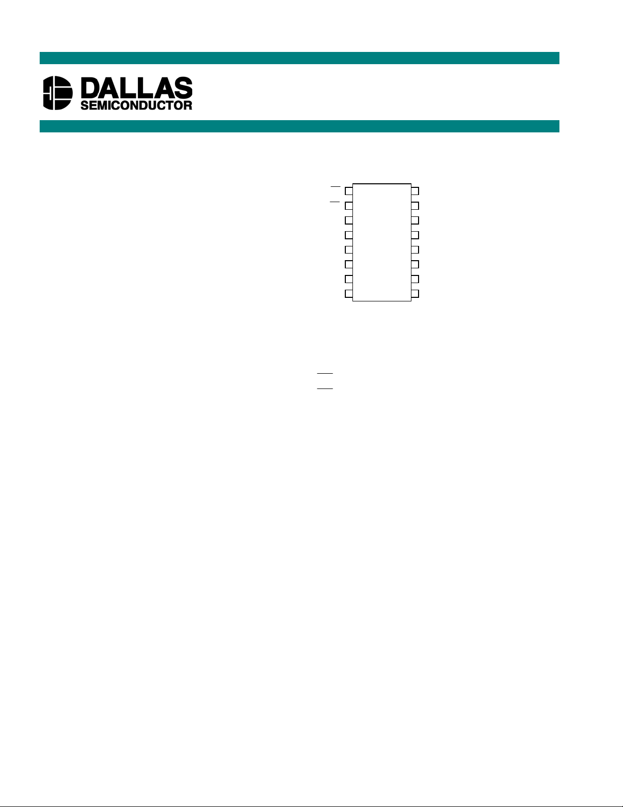
PIN ASSIGNMENT
UV VDD
1
1
CC
2
2
VCH
SNS
SNS
SNS
NC
IS2
3
2
4
5
6
7
8
DS2770
16-Pin TSSOP
16
15
14
13
12
11
10
VIN
DQ
VSS
VSS
VSS
NC
IS1
9
PIN DESCRIPTION
UV – Battery Undervoltage Detect Output
CC – Charge Control Output
VCH – Charge Supply Input
SNS – Sense Resistor Connection
IS2 – Current-Sense Input
IS1 – Current-Sense Input
VSS – Device Ground
DQ – Data Input/Output
VIN – Voltage Sense Input
VDD – Power Supply Input
NC – No Connect
ORDERING INFORMATION
ORDERING NUMBER MARKING DESCRIPTION
DS2770AE D2770EA TSSOP, Ext. Sense Res., 4.1V Charge Voltage
DS2770BE D2770EB TSSOP, Ext. Sense Res., 4.2V Charge Voltage
DS2770AE/T&R D2770EA DS2770AE on Tape & Reel
DS2770BE/T&R D2770EB DS2770BE on Tape & Reel
DS2770AE-025 2770EAR TSSOP, 25mW Sense Res., 4.1V Charge Voltage
DS2770BE-025 2770EBR TSSOP, 25mW Sense Res., 4.2V Charge Voltage
DS2770AE-025/T&R 2770EAR DS2770AE-025 on Tape & Reel
DS2770BE-025/T&R 2770EBR DS2770BE-025 on Tape & Reel
1-Wire is a registered trademark of Dallas Semiconductor.
1 of 27 041202
Page 2

DS2770
DESCRIPTION
The DS2770 battery monitor and charge controller performs several functions needed for thorough
battery maintenance. When used in conjunction with the host system’s processor, a battery-pack resident
DS2770 may be utilized for applications that include charging, remaining capacity estimation, safety
monitoring, and nonvolatile (NV) parametric storage.
The DS2770 provides a unique ID, a digital temperature sensor, an analog-to-digital converter (ADC) that
measures battery voltage and current, an integrated current accumulator that keeps a running total of all
current entering and leaving the battery, an elapsed time meter, NV memory for storage of important
parameters, and an integrated charge controller supporting rechargeable lithium (including lithium-ion
and lithium-ion polymer) and nickel metal hydride (NiMH) batteries. Current measurement can be
accomplished through the use of an integrated 25mW sense resistor or through an external sense resistor.
The resolution of the current, voltage, and temperature measurements is sufficient for process monitoring
applications such as battery-charge control and safety. The charge-control technique is user-selectable to
support either pulse charge for rechargeable lithium or dT/dt termination for NiMH. Additionally,
programmable charge timers and low-battery recovery are provided for safety and convenience.
Information is sent to/from the DS2770 over a 1-Wire interface so that only one wire (and ground) needs
to be connected from a processor to a DS2770. This means that DS2770-equipped battery packs need
only four output connectors: battery power, charge source, ground, and the 1-Wire interface. Each device
has a factory-programmed 64-bit net address that allows it to be individually addressed by the host
system.
Two types of memory are provided on the DS2770 for battery information storage: lockable EEPROM
and SRAM. EEPROM memory saves important battery data in true NV memory that is unaffected by
severe battery depletion, accidental shorts, or ESD events and becomes ROM when locked to provide
additional security for unchanging battery data. SRAM provides inexpensive storage for temporary data.
2 of 27
Page 3
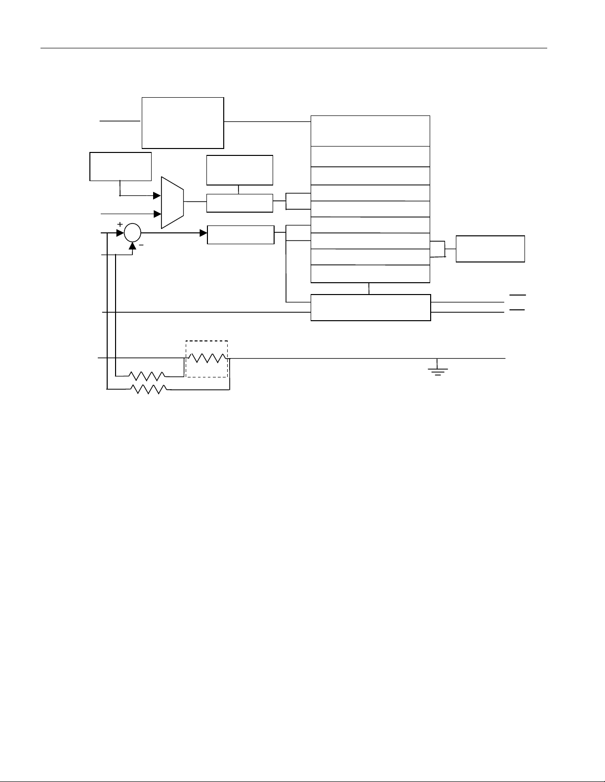
BLOCK DIAGRAM Figure 1
1-WIRE
DQ
INTERFACE
AND
ADDRESS
DS2770
REGISTERS AND
USER MEMORY
VIN
IS1
IS2
VCH
SNS
THERMAL
SENSE
VOLTAGE
REFERENCE
MUX
Internal sense resistor configuration only
25m
ADC
ADC
W
LOCKABLE EEPROM
SRAM
TEMPERATURE
VOLTAGE
CURRENT
ACCUM CURRENT
TIMEBASE
TIMER
STATUS/CONTROL
CC
CHARGE CONTROL
UV
CHIP GROUND
VSS
3 of 27
Page 4

DETAILED PIN DESCRIPTION Table 1
PIN SYMBOL DESCRIPTION
DS2770
1
UV
Battery Undervoltage Detect Output: This pin allows charge of the
battery at a reduced rate when the battery cell voltage is less than the low
battery voltage threshold, V
2
CC
Charge Control Output: Charge of the battery is controlled through this
pin when battery cell voltage is greater than or equal to V
3VCH
Charge Supply Input: The charge source is connected to this pin and is
LB
.
.
LB
measured by the DS2770 to determine if a charge source is present.
4, 5, 6 SNS Sense Resistor Connection: Connect to the negative terminal of the
battery pack. In the internal sense resistor configuration, the sense resistor
is connected between VSS and SNS.
8IS2
Current-Sense Input: This pin is internally connected to SNS through a
W resistor. Connect a 0.1mF capacitor between IS2 and IS1 to
10k
complete a lowpass filter.
9IS1Current-Sense Input: This pin is internally connected to VSS through a
W resistor. Connect a 0.1mF capacitor between IS1 and IS2 to
10k
complete a lowpass filter.
11, 12, 13 VSS
Device Ground: Connect directly to the negative terminal of the battery
cell. For the external sense resistor configuration, connect the sense
resistor between VSS and SNS.
14 DQ Data Input/Out: 1-Wire data line. Open-drain output driver. Connect this
pin to the DATA terminal of the battery pack. Pin has an internal pulldown for sensing disconnection.
15 VIN
Voltage Sense Input: The voltage on the battery cell is monitored via this
input pin.
16 VDD Power Supply Input: Input supply voltage for the DS2770 (2.7V to
5.5V)
7, 10 NC
Do not connect.
4 of 27
Page 5
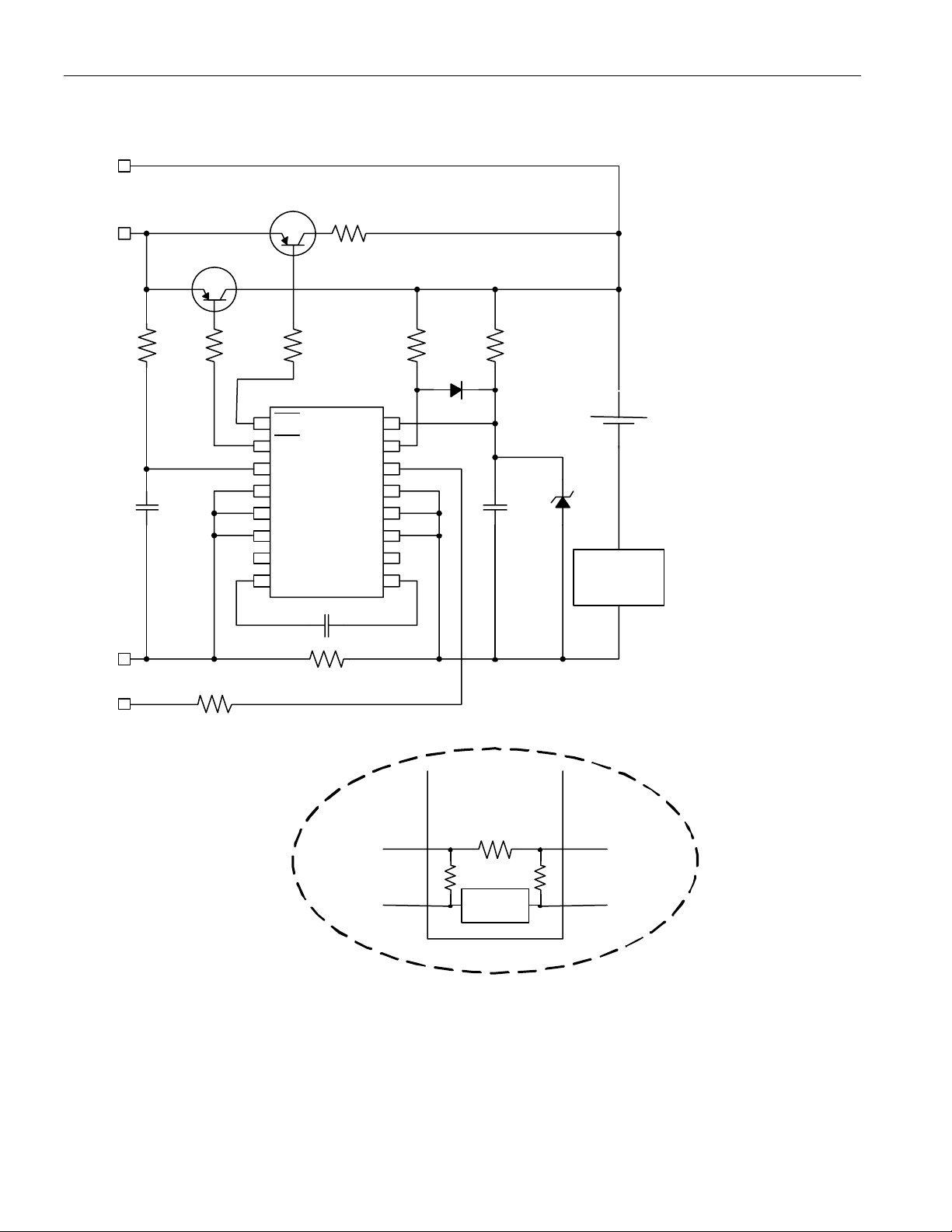
APPLICATION EXAMPLE Figure 2
PACK+
DS2770
CHARGE
SOURCE
4403
FMMT718
360W
4.7kW 1kW1kW100W150W
UV
CC
VCH
0.1mF0.1mF
SNS
SNS
SNS
NC
IS2
VDD
VIN
DQ
VSS
VSS
VSS
NC
IS1
0.1mF
5.1V
Lithium
Protection
Circuit
PACK-
DATA
1 — R
2 — R
(1)
R
SNS
150W
DS2770
R
SNS-INT
IS2 IS1
is present for external sense resistor configuration only.
SNS
is present for internal sense resistor configuration only.
SNS-INT
10KW
Voltage
Sense
(2)
VSSSNS
10KW
5 of 27
Page 6

DS2770
POWER MODES
The DS2770 has two possible power modes: Active Mode and Sleep Mode. While in Active Mode, the
DS2770 continually measures current, voltage, temperature, and time. Also, current flow is accumulated,
charge control is provided, and data is available to the host system. In Sleep Mode, the DS2770 ceases
these activities. The DS2770 can enter Sleep Mode only when the PMOD bit in the Status Register is set
to 1 and the following other conditions occur:
§ The CINI bit is set to 0 and the DQ line is held low for longer than two seconds. If a charge is in
progress, charging will immediately stop and the device will begin transition to Sleep Mode.
§ The CINI bit is set to 1 and the DQ line is held low for longer than two seconds. If a charge is in
progress, the DS2770 will not go into Sleep Mode until the charge operation is completed.
The DS2770 returns to Active Mode when any of the following occurs:
§ The DQ line is pulled high.
§ The voltage on VCH becomes greater than VDD (charger connection) with the CINI bit set to 1.
Once the DS2770 identifies the 2 second DQ low condition, a transition to Sleep Mode begins. This
process will take up to an additional 11 seconds before the supply current drops to I
The DS2770 defaults to Active Mode when power is first applied to VDD.
SLEEP
levels.
CHARGER FUNCTION
The DS2770 operates as a standalone charge controller supporting rechargeable lithium and NiMH
battery technologies. The battery type to be charged is selectable through the CTYPE bit of the Status
Register (0 for rechargeable lithium and 1 for NiMH). Charge control of both battery types is performed
by on/off gating of an external constant current or current-limited charge source. If the battery voltage is
less than V
battery at a reduced rate before fast charging can begin. In Figure 2’s application circuit,
trickle-charge current limited by a 360
characteristics of the charge source.
including pack temperature and the status of the CINI bit.
reaches V
respectively, in the CSTAT1 and CSTAT0 bits of the Status Register assuming any previous charge
sequence completed status has been cleared.
Fast charging can be initiated by one of two methods:
1) Issuing a Start Charge command [B5h].
2) Introducing a charge supply on the VCH pin when the CINI bit in the Status Register is a 1.
Note that if VDD is below approximately 1.8V prior to using either initiation method, fast charge will not
start after the battery is trickle charged to V
and a charge source is present, pin UV is driven low, signifying the need to recover the
LB
UV gates a
W series resistor. Selection of this resistor depends on the
UV is driven low independent of any other state of the pack,
UV is driven high when the battery voltage
. While trickle charging, a “charge in progress” status is indicated with (0, 1) values,
LB
.
LB
After initiation, the start of fast charge may be postponed if any of the following conditions exist:
§ The temperature is outside the valid charge window specified by T
(0°C) and TCH (40°C).
CL
§ Charge source is not present (VCH < VDD).
§ Conversion data is not valid (data becomes valid 110ms after waking from Sleep Mode).
§ Battery voltage is less than the low-battery-voltage threshold, V
6 of 27
, (3.0V).
LB
Page 7

DS2770
After initiation and clearing of the above conditions, fast charging begins with the CC pin driven low.
During fast charging,
which
CC is driven high for approximately 27ms every 55ms. As long as the charge source remains
CC remains low, except for periodic testing of premature charge source removal in
connected and the temperature remains in the valid range, charging will proceed per the method selected
by the CTYPE bit. If the charge source is removed or the Stop Charge command [BEh] is issued,
CC is
driven high and charging must be reinitiated by one of the two charge initiation methods described
previously. Charging will also be stopped if the DQ line is low for >2s and the CINI bit is set to 0.
Assuming any previous charge status has been cleared, a “charge in progress” status is indicated during
fast charging with (0, 1) values, respectively, in the CSTAT1 and CSTAT0 bits of the Status Register.
Upon charge completion according to the method selected with the CTYPE bit, or completion due to
either of the secondary methods, pin
CC will return to the high state, and a charge done condition will be
flagged with (1, 1) values in the CSTAT1 and CSTAT0 bits of the Status Register. Note that the charge
done status is latched and must be cleared by a write of any value to the Status Register. Once charging
has been completed or aborted, the DS2770 may either enter the Sleep Mode or remain active, depending
on the state of the PMOD bit described previously in the Power Modes section.
RECHARGEABLE LITHIUM CHARGER OPERATION
Fast charging of lithium cell types is performed in two distinct regions. The bulk charge region delivers
most of the charge to the cell by gating current from the charge source while the battery voltage is below
the charge voltage threshold, V
switch. When the battery voltage reaches V
is employed that allows
CC to remain low for a delay period of t
high. When the battery voltage decays below V
pulse region of charge continues with the
. The CC pin remains low, driving a PNP or P-channel MOSFET
CV
, the pulse region begins in which a pulse-charge technique
CV
(875ms) after which CC is driven
VCV
, CC is again driven low and the cycle is repeated. The
CV
CC duty cycle slowly changing. Eventually, the battery voltage
decay time, and thus the
charge decay time limit, t
CC high time, becomes longer than 13.125s, and charge is terminated. The
, includes one 875ms period of CC low and 15 periods high for a total time of
CD
14s. The average charge rate at termination is 1/16 of the rate set by the charge source. See Figure 3 for
an illustration of the t
decay method. See the Secondary Charge Termination section for the secondary
CD
termination means based on time or temperature included for increased safety.
7 of 27
Page 8
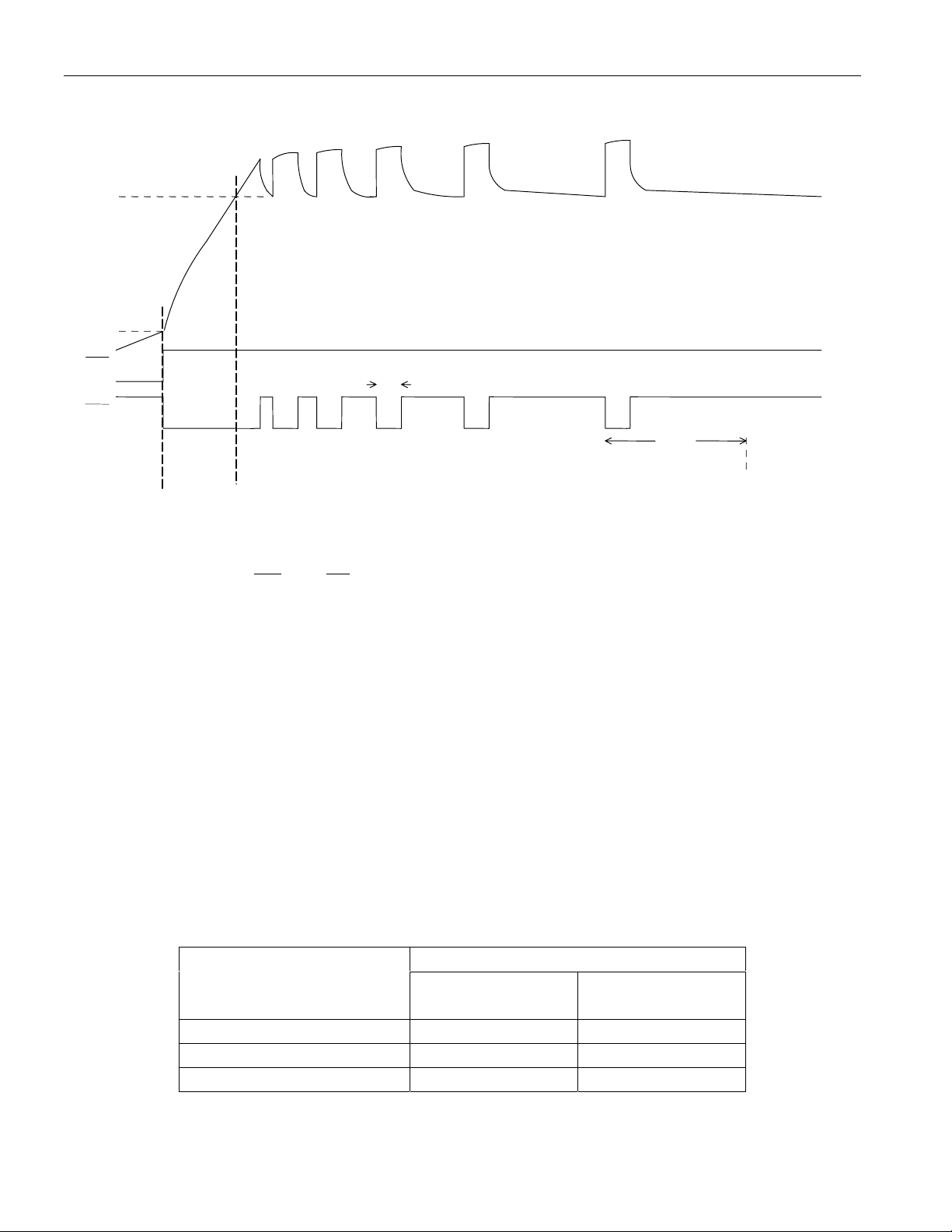
RECHARGEABLE LITHIUM PULSE CHARGING Figure 3
V
CV
VIN
V
LB
DS2770
UV
t
VCV
CC
t
Trickle
Charge
Bulk
Region
Pulse
Region
Pulse Charge
CD
Charge
Complete
NiMH CHARGER OPERATION
During NiMH charging, charge current from a constant current or current-limited supply is gated to the
battery under control of
when the battery reaches 3.0V, a three-cell NiMH battery will begin fast charge at 1.0V per cell. A
voltage divider can be used to adjust the transition point to a higher per cell voltage, though values in the
Voltage Measurement Register would be affected by the divider ratio.
At the start of fast charge, the DS2770 uses the most recent temperature measurement to determine the
appropriate dT/dt termination rate for the ambient conditions from Table 2 below. During the first 5
minutes, temperature rate termination is blanked to avoid false dT/dt detection due to I
the blanking period, dT/dt detection begins using one of the initial rates from Table 2 and requires that the
rate of temperature rise continue at or above the selected rate for 2.8 minutes. Internally, values from the
Temperature Measurement Register are averaged in determining the sustained rate of temperature rise.
The effective rate shown in Table 2 is based on NiMH charge data and represents the predicted
instantaneous dT/dt rate at termination.
UV and CC pins. Since the transition from trickle charge to fast charge occurs
2
R heating. After
NiMH CHARGE TERMINATION THRESHOLDS Table 2
dT/dt THRESHOLDAMBIENT
TEMPERATURE (°C)
0 to +5 0.30 1.0
+5 to +15 0.45 1.0
+15 to +40 0.60 1.0
INITIAL
(°C/MIN)
8 of 27
EFFECTIVE
(°C/MIN)
Page 9
DS2770
SECONDARY CHARGE TERMINATION
Two secondary charge terminations are included. Independent of battery technology selection, charge
terminates if the maximum charge temperature is exceeded or the charge timer expires. The CSTAT1 and
CSTAT0 bits in the Status Register will both be set to 1 to indicate a “charge sequence completed” status.
The maximum temperature threshold, T
during charge, the charge is terminated.
T
MCT
, is fixed at +50°C. If the temperature measurement exceeds
MCT
The maximum charge time is set in the Charge Time Register, CTR. CTR is initialized from lockable
EEPROM location address 34h at the start of fast charge (
decrements by one count every 56 seconds (t
) during fast charge. If CTR reaches zero, charging is
CTR
CC driven low after initiation). CTR
terminated. Since CTR is writable, the value in CTR may be overwritten at any time during a charge to
modify the maximum charge time. Figure 4 shows the format of CTR.
CHARGE TIME REGISTER Figure 4
Address 06
272625242322212
0
MSb LSb
Units: 0.015625h
CURRENT MEASUREMENT
In the Active Mode of operation, the DS2770 continually measures the current flow into and out of the
battery by measuring the voltage drop across a current-sense resistor. The DS2770 is available in two
configurations: 1) internal 25m
either configuration, the DS2770 considers the voltage difference between pins IS1 and IS2 (V
) to be the filtered voltage drop across the sense resistor. A positive VIS value indicates current is
V
IS2
flowing into the battery (charging), while a negative V
battery (discharging). Note that when an external sense resistor is used, one end of the resistor must be
wired directly to VSS (the negative terminal of the cell) for proper operation of the current measurement
circuitry.
W current-sense resistor; 2) external user-selectable sense resistor. In
= V
IS
IS1
value indicates current is flowing out of the
IS
-
is measured with a signed resolution of 15 bits. Measurements are updated in the Current Register in
V
IS
two’s complement format every 3.52 seconds. The Current Register value represents the average current
over 3.52 seconds. Currents outside the register’s range are reported at the limit of the range. Figure 5
shows the format of the Current Register.
For the internal sense resistor configuration, the DS2770 maintains the Current Register in units of amps,
with a resolution of 62.5
mA and a full-scale range of ±2.048A. The DS2770 automatically compensates
for internal sense resistor process variations and temperature effects when reporting current.
For the external sense resistor configuration, the DS2770 writes the measured V
Register, with a resolution of 1.56
mV and a full-scale range of ±51.2mV.
9 of 27
voltage to the Current
IS
Page 10

CURRENT REGISTER FORMAT Figure 5
r
r
r
r
MSB—Address 0E LSB—Address 0F
DS2770
S2142132122112
1029
8
2
272625242322212
0
MSb LSb MSb LSb
Units: 62.5mAh for internal sense resisto
1.56mVh for external sense resisto
CURRENT ACCUMULATORS
The current accumulator facilitates remaining capacity estimation by tracking the net current flow into
and out of the battery. Current flow into the battery increments the current accumulator while current
flow out of the battery decrements it. Data is maintained in the current accumulator in two’s complement
format and updated every 3.52s. Figure 6 the format of the current accumulator.
When the internal sense resistor is used, the DS2770 maintains the current accumulator in units of amphours, with a resolution of 250
the DS2770 maintains the current accumulator in units of volt-hours, with a resolution of 6.25
full-scale range of
±205mVh.
mA and full-scale range of ±8.19Ah. When using an external sense resistor,
mVh and a
ACCUMULATED CURRENT REGISTER FORMAT Figure 6
MSB—Address 10 LSB—Address 11
S2142132122112
1029
8
2
272625242322212
0
MSb LSb MSb LSb
Units: 0.25mAh for internal sense resisto
6.25mVh for external sense resisto
CURRENT OFFSET COMPENSATION
Current measurement and consequently the current accumulation are internally compensated for offset on
a continual basis to minimize errors from variations in device temperature and supply voltage. Offset
compensation is corrected to ±1LSB at least once per hour. Additionally, the Current Offset Bias Register
provides a user-programmable constant bias value that may be used to correct for errors due to circuit
layout or topology that result in current measurement or current accumulation errors. It can also be used
to arbitrarily apply a constant bias to force the current measurement to be pessimistic, or correct for room
temperature self-discharge. The current offset bias value is stored in EEPROM addresses 32h and 33h in
two’s complement format. The stored value is subtracted from each current measurement; therefore,
positive values (0001h to 7fffh) bias the current measurement and current accumulation in the discharge
direction. Figure 7 shows the format of the Current Offset Bias Register.
10 of 27
Page 11

CURRENT-OFFSET BIAS Figure 7
r
r
MSB—Address 32 LSB—Address 33
DS2770
S2142132122112
1029
8
2
272625242322212
0
MSb LSb MSb LSb
Units: 0.0625mA for internal sense resisto
1.5625mV for external sense resisto
VOLTAGE MEASUREMENT
The DS2770 continuously measures the voltage between pins VIN and VSS with a resolution of 4.88mV
over a range of 0V to 4.992V. Measurement data is updated every 55ms and placed in the Voltage
Register in two’s complement format. Voltages above the maximum register value are reported as the
maximum value. Figure 8 shows the Voltage Register format.
VOLTAGE REGISTER FORMAT Figure 8
MSB—Address 0C LSB—Address 0D
S2928272625242
MSb LSb MSb LSb
3
222120XXXXX
Units: 4.88mV
TEMPERATURE MEASUREMENT
The DS2770 uses an integrated temperature sensor to continually measure battery temperature with a
resolution of 0.125°C. Temperature measurements are updated every 55ms and placed in the Temperature
Register in two’s complement format. Figure 9 shows the Temperature Register format.
TEMPERATURE REGISTER FORMAT Figure 9
MSB—Address 18 LSB—Address 19
S2
9
28272625242
3
222120XXXXX
MSb LSb MSb LSb
Units: 0.125°C
TIMER
The DS2770 provides a general-purpose timer with a range of 1024h. The timer count is stored in the
Elapsed Time Register with a resolution of approximately 56s. The count will roll over to zero when it
reaches its maximum value and begin counting up again. Additionally, the user can write any desired
value to the register. Figure 10 shows the Elapsed Time Register format.
11 of 27
Page 12

ELAPSED TIME REGISTER FORMAT Figure 10
r
MSB—Address 02 LSB—Address 03
DS2770
2152142132122112
1029
8
2
272625242322212
0
MSb LSb MSb LSb
Units: 0.015625h
MEMORY
The DS2770 has a 256-byte linear address space with registers for instrumentation, status, and control in
the lower 32 bytes, with lockable EEPROM and SRAM memory occupying portions of the remaining
address space. All EEPROM and SRAM memory is general purpose except addresses 31h, 32h, 33h, and
34h, which should be written with the default values for the Status Register (31h), Current Offset Register
(32h to 33h), and Charge Time Register (34h). When the MSB of any two-byte register is read, both the
MSB and LSB are latched and held for the duration of the Read Data command to prevent updates during
the read and ensure synchronization between two register bytes. For consistent results, always read the
MSB and the LSB of a two-byte register during the same Read Data command sequence.
EEPROM memory is shadowed by RAM to eliminate programming delays between writes and to allow
the data to be verified by the host system before being copied to EEPROM. All reads and writes to/from
EEPROM memory actually access shadow RAM. In unlocked EEPROM blocks, the Write Data
command updates shadow RAM. In locked EEPROM blocks, the Write Data command is ignored. The
Copy Data command copies the contents of shadow RAM to EEPROM in an unlocked block of
EEPROM, but has no effect on locked blocks. The Recall Data command copies the contents of a block
of EEPROM to shadow RAM.
Lockable EEPROM is byte programmable and functions as EEPROM until reprogramming is disabled by
the user. The lockable EEPROM can be locked in separate blocks and operate as general EEPROM until
locked by the Lock command [6Axxh]. Reprogramming of the lockable EEPROM blocks is permanently
disabled once the Lock command is used. Addresses 20 to 2Fh comprise a first 16-byte block, addresses
30 to 3Fh comprise a second 16-byte block, and addresses 40 to 47h comprise a third 8-byte block.
Within the second block, address 31h holds the Status Register initialization data, addresses 32h and 33h
hold the Current Offset Register, and address 34h holds the Charge Time Register initialization data. The
Status Register initialization data is supplied to the Status Register in location address 01h on either a
device power up or upon the execution of the Refresh command [63h]. The charge time initialization data
is supplied to the Charge Time Register in address 06h upon the start of fast charge. The Status Register
and the Charge Time Register are both initialized directly from the EEPROM and not from the shadow
RAM. However, the current offset data is supplied directly from the shadow RAM. See the sections on
the Status Register and the Charge Time Register for more detailed information. See the detailed Memory
Map in Figure 11 for more information on the DS2770 memory.
12 of 27
Page 13

DS2770
MEMORY MAP Figure 11
ADDRESS (HEX) DESCRIPTION R/W
00 Reserved
01 Status Register R**
02 Elapsed Time Register MSB R/W
03 Elapsed Time Register LSB R/W
04 to 05 Reserved
06 Charge Time Register R/W
07 EEPROM Register R/W
08 to 0B Reserved
0C Voltage Register MSB R
0D Voltage Register LSB R
0E Current Register MSB R
0F Current Register LSB R
10 Accumulated Current Register MSB R/W
11 Accumulated Current Register LSB R/W
12 to 17 Reserved
18 Temperature Register MSB R
19 Temperature Register LSB R
1A to 1F Reserved
20 to 2F Lockable EEPROM Block 0 R/W*
30 to 3F Lockable EEPROM Block 1
(31 = Status Register Initialization)
(32 to 33 = Current Offset Register)
(34 = Charge Time Register Initialization)
40 to 47 Lockable EEPROM Block 2 R/W*
48 to 7F Reserved
80 to 8F General-Purpose SRAM R/W
90 to FF Reserved
* The lockable EEPROM address locations 20h through 47h are writeable until locked by using the Lock
function command [6Axxh], after which it is read only.
** The Status Register bits are read only. However, writing any byte value to the Status Register is
required to clear a previous charge completion condition flagged with both CSTAT1, CSTAT0 bits set.
R/W*
STATUS REGISTER
The default values for the Status Register are stored in lockable EEPROM in the corresponding bits of
address 31h. These values in address location 31h are supplied directly to the Status Register (not from
shadow RAM) on either a device power-up or upon execution of the Refresh command. Changes to the
Status Register bits must be made to the EEPROM location 31h, and then use the Refresh command to
recall the changes to the Status Register. Figure 12 shows the format of the Status Register. The function
of each bit is described in detail in the following paragraphs.
13 of 27
Page 14

DS2770
STATUS REGISTER FORMAT Figure 12
Address 01
bit 7 bit 6 bit 5 bit 4 bit 3 bit 2 bit 1 bit 0
CSTAT1 CSTAT0 PMOD RNAOP X X CINI CTYPE
CSTAT1, CSTAT0 — Charge Status. The CSTAT1 and CSTAT0 bits indicate the status of charge per
the table below:
CSTAT1 CSTAT0 STATUS
0 0 No charge source present
0 1 Charge in progress
1 0 Charge source is present
1 1 Charge sequence completed
The charge sequence complete state (1, 1) is present until cleared by a write to the Status Register.
PMOD — Sleep Mode Enable. A value of 1 in this bit enables the DS2770 to enter Sleep Mode when the
DQ line goes low for greater than two seconds and leaves Sleep Mode when the DQ line goes high. A
value of 0 disables DQ-related transitions into and out of Sleep Mode. The desired default value should
be set in bit 5 of address location 31h. The factory default of the PMOD bit is 0.
RNAOP — Read Net Address Opcode. A value of 0 in this bit sets the opcode for the Read Net Address
command to 33h, while a 1 sets the opcode to 39h. The desired default value should be set in bit 4 of
address location 31h. The factory default of the RNAOP bit is 0.
CINI — Charge Initiation Select. The CINI bit is used to determine the method of charge initiation that
will be allowed. A value of 0 indicates that charge may be started only upon use of the Start Charge [B5h]
command. A value of 1 indicates that charge may be started by either the Start Charge command, or by
the application of a charge source at the charge supply input pin, VCH. The desired default value should
be set in bit 1 of address location 31h. The factory default of the CINI bit is 0.
CTYPE — Charge Type. The charge type bit indicates the Charge Mode that will be used during
charging. A 1 selects NiMH charger operation and a 0 selects rechargeable lithium charger operation. The
desired default value should be set in bit 0 of address location 31h. It is suggested that the EEPROM
block containing the Status Register initiation (location 31h) be locked once the CTYPE and other Status
Register bits are configured to avoid any possible unintended alterations during use. The factory default
of the CTYPE bit is 0.
X — Reserved Bits.
14 of 27
Page 15

DS2770
EEPROM REGISTER
Figure 13 shows the format of the EEPROM Register. The function of each bit is described in detail in
the following paragraphs.
EEPROM REGISTER FORMAT Figure 13
Address 07
bit 7 bit 6 bit 5 bit 4 bit 3 bit 2 bit 1 bit 0
EEC LOCK X X X BL2 BL1 BL0
EEC — EEPROM Copy Flag. A 1 in this read-only bit indicates that a Copy Data command is in
progress. While this bit is high, writes to EEPROM addresses are ignored. A 0 in this bit indicates that
data may be written to unlocked EEPROM blocks.
LOCK — EEPROM Lock Enable. This bit is used to enable the Lock command by writing a 1 to it prior
to issuing the command. When this bit is 0, the Lock command is ignored. After the Lock command is
executed, the Lock bit is reset to 0. The Lock bit will also be reset by any other command issued after the
bit has been set. The factory default is 0.
BL2 — EEPROM Block 2 Lock Flag. A 1 in this read-only bit indicates that EEPROM Block 2
(addresses 40 to 47h) is locked (read-only) while a 0 indicates Block 2 is unlocked (read/write).
BL1 — EEPROM Block 1 Lock Flag. A 1 in this read-only bit indicates that EEPROM Block 1
(addresses 30 to 3Fh) is locked (read-only) while a 0 indicates Block 1 is unlocked (read/write).
BL0 — EEPROM Block 0 Lock Flag. A 1 in this read-only bit indicates that EEPROM Block 0
(addresses 20 to 2Fh) is locked (read-only) while a 0 indicates Block 0 is unlocked (read/write).
X — Reserved Bits.
1-WIRE BUS SYSTEM
The 1-Wire bus is a system that has a single bus master and one or more slaves. A multidrop bus is a
1-Wire bus with multiple slaves. A single-drop bus has only one slave device. In all instances, the
DS2770 is a slave device. The bus master is typically a microprocessor in the host system. The discussion
of this bus system consists of four topics: 64-bit Net Address, Hardware Configuration, Transaction
Sequence, and 1-Wire Signaling.
64-BIT NET ADDRESS
Each DS2770 has a unique factory-programmed 1-Wire net address that is 64 bits in length. The first
eight bits are the 1-Wire family code (2Eh for DS2770). The next 48 bits are a unique serial number. The
last eight bits are a CRC of the first 56 bits (see Figure 14). The 64-bit net address and the 1-Wire I/O
circuitry built into the device enable the DS2770 to communicate through the 1-Wire protocol detailed in
the 1-Wire Bus System section of this data sheet.
15 of 27
Page 16

DS2770
NET ADDRESS FORMAT Figure 14
8-Bit CRC 48-Bit Serial Number 8-Bit Family
Code (2Eh)
CRC GENERATION
The DS2770 has an 8-bit CRC stored in the most significant byte of its 64-bit net address. To ensure
error-free transmission of the address, the host system can compute a CRC value from the first 56 bits of
the address and compare it to the CRC from the DS2770. The host system is responsible for verifying the
CRC value and taking action as a result. The DS2770 does not compare CRC values and does not prevent
a command sequence from proceeding as a result of a CRC mismatch. Proper use of the CRC can result
in a communication channel with a very high level of integrity.
The 1-Wire CRC can be generated by the host using a circuit consisting of a Shift Register and XOR
gates as shown in Figure 15, or it can be generated in software. Additional information about the Dallas
1-Wire Cyclic Redundancy Check is available in
Redundancy Checks with Dallas Semiconductor Touch Memory Products.
Application Note 27, Understanding and Using Cyclic
In Figure 15, the Shift Register bits are initialized to 0. Then, starting with the least significant bit of the
th
family code, one bit at a time is shifted in. After the 8
th
number is entered. After the 48
bit of the serial number has been entered, the Shift Register contains the
bit of the family code has been entered, the serial
CRC value.
1-WIRE CRC GENERATION BLOCK DIAGRAM Figure 15
input
MSb
XOR XOR
LSb
XOR
HARDWARE CONFIGURATION
Because the 1-Wire bus has only a single line, it is important that each device on the bus be able to drive
it at the appropriate time. To facilitate this, each device attached to the 1-Wire bus must connect to the
bus with open-drain or tristate output drivers. The DS2770 uses an open-drain output driver as part of the
bidirectional interface circuitry shown in Figure 16. If a bidirectional pin is not available on the bus
master, separate output and input pins can be tied together.
The 1-Wire bus must have a pull-up resistor at the bus-master end of the bus. For short line lengths, the
value of this resistor should be approximately 5k
W. The idle state for the 1-Wire bus is high. If, for any
reason, a bus transaction must be suspended, the bus must be left in the idle state in order to properly
resume the transaction later. If the bus is left low for more than 120
ms, slave devices on the bus begin to
interpret the low period as a reset pulse, effectively terminating the transaction.
16 of 27
Page 17

1-WIRE BUS INTERFACE CIRCUITRY Figure 16
DS2770
BUS MASTER DS2770 1-WIRE PORT
R
X
T
X
2.0V < V
RX = Receive
T
< 5.5V
PULLUP
= Transmit
X
A
I
PD
Typ.
TRANSACTION SEQUENCE
The protocol for accessing the DS2770 through the 1-Wire port is as follows:
§ Initialization
§ Net Address command
§ Function command
§ Transaction/Data
R
X
T
X
The sections that follow describe each of these steps in detail.
All transactions of the 1-Wire bus begin with an initialization sequence consisting of a reset pulse
transmitted by the bus master followed by a presence pulse simultaneously transmitted by the DS2770
and any other slaves on the bus. The presence pulse tells the bus master that one or more devices are on
the bus and ready to operate. For more details, see the 1-Wire Signaling section.
NET ADDRESS COMMANDS
Once the bus master has detected the presence of one or more slaves, it can issue one of the five Net
Address commands described in the following paragraphs. The name of each Net Address command is
followed by the 8-bit opcode for that command in square brackets. Figure 17 presents a transaction
flowchart of the five Net Address commands.
Read Net Address [33h or 39h]. This command allows the bus master to read the DS2770’s 1-Wire net
address. This command can only be used if there is a single slave on the bus. If more than one slave is
present, a data collision occurs when all slaves try to transmit at the same time (open drain produces a
wired-AND result). The RNAOP bit in the Status Register selects the opcode for this command, with
RNAOP = 0 indicating 33h and RNAOP = 1 indicating 39h.
Match Net Address [55h]. This command, followed by a 64-bit net address, allows the bus master to
specifically address one DS2770 on the 1-Wire bus. Only the DS2770 that exactly matches the 64-bit
address responds to the subsequent Function command. All other slaves ignore the Function command
and wait for a reset pulse. This command can be used with one or more slave devices on the bus.
17 of 27
Page 18

DS2770
Skip Net Address [CCh]. This command saves time when there is only one DS2770 on the bus by
allowing the bus master to issue a Function command without specifying the net address of the slave. If
more than one slave device is present on the bus, a subsequent Function command can cause a data
collision when all slaves transmit data at the same time.
Search Net Address [F0h]. This command allows the bus master to use a process of elimination to
identify the net addresses of all slave devices on the bus. The search process involves the repetition of a
simple three-step routine: read a bit, read the complement of the bit, then write the desired value of that
bit. The bus master performs this simple three-step routine on each bit of the net address. After one
complete pass through all 64 bits, the bus master knows the address of one device. The remaining devices
can then be identified on additional passes. See Chapter 5 of
The Book of DS19xx iButton Standards for a
comprehensive discussion of a net address search, including an actual example. The Search Net Address
algorithm cannot be used with the DS2770 in multi-drop applications with any 1-Wire devices that have
either a 6h or Eh as the LS byte of the 1-Wire family code. Because the 1-Wire family code of the
DS2770 is 2Eh, Search Net Address cannot be used to ascertain the 64-bit serial numbers of multiple
DS2770’s on a single bus. If an application does require two DS2770 to share a common bus, the bus
master may determine the serial numbers of each device using the Read Net Address function, with one
part configured to respond to the 33h command (RNAOP = 0) and the other the 39h command (RNAOP
= 1).
Resume [A5h]. This command is used to speed data throughput in multidrop environments where the
DS2770 needs to be accessed several times. The DS2770 contains an internal flag that, when set, directly
transfers control to the memory function commands upon receipt of a Resume command, similar to the
Skip Net Address command. The only way the internal flag is set is through successfully executing the
Match Net Address command or Search Net Address command. Once the flag is set, the device can
repeatedly be accessed through the Resume command function. Accessing another device on the bus will
clear the flag, thus preventing two or more devices from simultaneously responding to the Resume
command function.
FUNCTION COMMANDS
After successfully completing one of the five Net Address commands, the bus master can access the
features of the DS2770 with any of the Function commands described in the following paragraphs. The
name of each function is followed by the 8-bit opcode for that command in square brackets.
Read Data [69h, XX]. This command reads data from the DS2770 starting at memory address XX. The
LSb of the data in address XX is available to be read immediately after the MSb of the address has been
entered. Because the address is automatically incremented after the MSb of each byte is received, the LSb
of the data at address XX+1 is available to be read immediately after the MSb of the data at address XX.
If the bus master continues to read beyond address FFh, the DS2770 will start over at address 00h.
Addresses labeled “reserved” in the memory map contain undefined data. The Read Data command may
be terminated by the bus master with a reset pulse at any bit boundary.
iButton is a registered trademark of Dallas Semiconductor.
18 of 27
Page 19

DS2770
Write Data [6Ch, XX]. This command writes data to the DS2770 starting at memory address XX. The
LSb of the data to be stored at address XX can be written immediately after the MSb of the address has
been entered. Because the address is automatically incremented after the MSb of each byte written, the
LSb to be stored at address XX+1 can be written immediately after the MSb to be stored at address XX. If
the bus master continues to write beyond address FFh, the DS2770 will start over-writing at address 00h.
Writes to read-only addresses, reserved addresses, and locked EEPROM blocks are ignored. Incomplete
bytes are not written. Writes to unlocked EEPROM blocks are to shadow RAM rather than EEPROM.
See the Memory section for more details.
Copy Data [48h, XX]. This command copies the contents of shadow RAM to EEPROM for the
EEPROM block beginning with address XX (20h for block 0, 30h for block 1, and 40h for block 2). Copy
Data commands that address locked blocks are ignored. While the Copy Data command is executing, the
EEC bit in the EEPROM Register is set to 1 and writes to EEPROM addresses are ignored. Reads and
writes to non-EEPROM addresses can still occur while the copy is in progress. The Copy Data command
takes t
time to execute.
EEC
Recall Data [B8h, XX]. This command recalls the contents of the EEPROM block containing the first
address location found in the block to shadow RAM.
Lock [6Ah, XX]. This command locks (write-protects) blocks of EEPROM whose first memory location
is XX (20h for block 0, 30h for block 1, and 40h for block 2). The Lock bit in the EEPROM Register
must be set to 1 before the Lock command is executed. The Lock command must be the next command
issued (after the 1-Wire reset) once the Lock bit has been set. If the Lock bit is 0, the Lock command has
no effect. The Lock command is permanent; a locked block can never be written again. The Lock
command takes t
time to execute.
EEC
Refresh [63h]. The Refresh command restores the Status Register initialization data stored in address
location 31h to the Status Register. The Status Register is initialized directly from the EEPROM and not
from the shadow RAM.
Start Charge [B5h]. The Start Charge command is used to initiate charge through the host interface.
Stop Charge [BEh]. The Stop Charge command is used to terminate charge through the host interface.
19 of 27
Page 20
ROM COMMAND FLOW CHART Figure 17
g
MASTER Tx
RESET PULSE
DS2770 Tx
PRESENCE PULSE
MASTER Tx
NET ADDRESS
COMMAND
DS2770
33h or 39h
READ
DS2770 Tx
FAMILY CODE
1 BYTE
DS2770 Tx
SERIAL NUMBER
6 BYTES
DS2770 Tx
CRC
1 BYTE
NO NO NO
55h
MATCH
MASTER Tx
BIT 0
BIT 0
MATCH?
MASTER Tx
BIT 1
BIT 1
MATCH?
NO NO
NO NO
F0h
SEARCH
YESYESYES
DS2770 Tx BIT 0
DS2770 Tx BIT 0
MASTER TX BIT 0
BIT 0
MATCH?
YESYES
DS2770 Tx BIT 1
DS2770 Tx BIT 1
MASTER TX BIT 1
BIT 1
MATCH?
YESYES
CCh
SKIP
YES
MASTER Tx
FUNCTION
COMMAND
NO
A5h
RESUME
YES
RESUME
FLAG SET?
YES
MASTER Tx
FUNCTION
COMMAND
NO
NO
MASTER Tx
FUNCTION
COMMAND
MASTER Tx
BIT 63
DS2770 Tx BIT 63
DS2770 Tx BIT 63
MASTER TX BIT 63
Clear Resume
Flag
Set Resume
YES
BIT 63
MATCH ?
Fla
NO
20 of 27
Page 21

FUNCTION COMMANDS Table 3
COMMAND DESCRIPTION
Reads data from
Read Data
Write Data
Copy Data
Recall Data
Lock
Refresh
Start Charge
Stop Charge
memory map starting
at address XX
Writes data to memory
starting at address XX 6Ch, XX Master Tx Unlimited
Copies shadow RAM
data to EEPROM
block that begins with
address location XX
Recalls EEPROM
block that begins with
address location XX to
shadow RAM
Permanently locks the
block of lockable
EEPROM memory
that begins with
address location XX
Restores Status
Register initialization
data
Initiates charge
through the host
interface.
Terminates charge
through the host
interface.
COMMAND
PROTOCOL
BUS STATE AFTER
COMMAND
BUS DATA
PROTOCOL
69h, XX Master R
X
Unlimited
48h, XX Master Reset None
B8h, XX Master Reset None
6Ah, XX Master Reset None
63h Master Reset None
B5h Master Reset None
BEh Master Reset None
DS2770
I/O SIGNALING
The 1-Wire bus requires strict signaling protocols to insure data integrity. The DS2770 uses the following
four protocols: the initiation sequence (reset pulse followed by presence pulse), Write 0, Write 1, and
Read Data. All of these types of signaling except the presence pulse are initiated by the bus master.
Figure 18 shows the initialization sequence required to begin any communication with the DS2770. A
presence pulse following a reset pulse indicates the DS2770 is ready to accept a Net Address command.
The bus master transmits (T
Receive Mode (R
). The 1-Wire bus line is then pulled high by the pull-up resistor. After detecting the
X
) a reset pulse for t
X
rising edge on the DQ pin, the DS2770 waits for the t
. The bus master then releases the line and goes into
RSTL
and then transmits the presence pulse for t
PDH
21 of 27
PDL
.
Page 22

DS2770
1-WIRE INITIALIZATION SEQUENCE (RESET PULSE AND PRESENCE
PULSE) Figure 18
DQ
V
CC
GND
t
RSTL
LINE TYPE LEGEND:
Both bus master and
DS2770 active low
t
PDH
t
PDL
t
RSTH
Resistor pullup
WRITE TIME SLOTS
A write time slot is initiated when the bus master pulls the 1-Wire bus from a logic high (inactive) level to
a logic low level. There are two types of write time slots: Write 1 and Write 0. All write time slots must
be t
(60µs to 120µs) in duration with a 1µs minimum recovery time, t
SLOT
DS2770 samples the 1-Wire bus line between 15µs and 60µs after the line falls. If the line is high when
sampled, a Write 1 occurs. If the line is low when sampled, a Write 0 occurs (see Figure 19). For the bus
master to generate a Write 1 time slot, the bus line must be pulled low and then released, allowing the line
to be pulled high within 15µs after the start of the write time slot. For the host to generate a Write 0 time
slot, the bus line must be pulled low and held low for the duration of the write time slot.
, between cycles. The
REC
READ TIME SLOTS
A read time slot is initiated when the bus master pulls the 1-Wire bus line from a logic high level to logic
low level. The bus master must keep the bus line low for at least 1µs and then release it to allow the
DS2770 to present valid data. The bus master can then sample the data t
read time slot. By the end of the read time slot, the DS2770 releases the bus line and allows it to be pulled
high by the external pull-up resistor. All read time slots must be t
1µs minimum recovery time, t
, between cycles. See Figure 19 for more information.
REC
(60µs to 120µs) in duration with a
SLOT
(15µs) from the start of the
RDV
22 of 27
Page 23

1-WIRE WRITE AND READ TIME SLOTS Figure 19
SLO
SLO
0
C
SLO
SLO
C
WRITE 0 SLOT WRITE 1 SLOT
t
T
t
LOW
t
RE
DQ
V
CC
GND
t
LOW1
DS2770
t
T
DQ
GND
DS2770 Sample Window
MIN TYP MAX
15ms15ms 30ms
READ 0 SLOT READ 1 SLOT
t
T
V
CC
Master Sample Window Master Sample Window
t
RDV
LINE TYPE LEGEND:
Both bus master and
DS2770 active low
>1ms
>1ms
t
RE
t
RDV
DS2770 Sample Window
MIN TYP MAX
15ms15ms 30ms
t
T
Resistor pullup
23 of 27
Page 24

DS2770
ABSOLUTE MAXIMUM RATINGS*
Voltage on VIN, Relative to Ground -0.3V to V
Voltage on VCH,
CC, UV -0.3V to +18V
Voltage on Any Other Pin, Relative to Ground -0.3V to +6V
Current Max Iol
CC, UV 20mA
Continuous Internal Sense Current ±2.5A
Pulsed Internal Sense Current ±50A for <100
Operating Temperature Range -40°C to +85°C
Storage Temperature Range -55°C to +125°C
Soldering Temperature See IPC/JEDEC J-STD-020A Specification
* This is a stress rating only and functional operation of the device at these or any other conditions above
those indicated in the operation sections of this specification is not implied. Exposure to absolute
maximum rating conditions for extended periods of time may affect reliability.
+ 0.3V
DD
ms/sec, <1000 pulses
RECOMMENDED DC
OPERATING CONDITIONS
(-20°C to +70°C, 2.7V £ V
£ 5.5V)
DD
PARAMETER SYMBOL MIN TYP MAX UNITS NOTES
Supply Voltage V
DD
2.7 5.5 V 1
Data Pin DQ -0.3 5.5 V 1
DC ELECTRICAL CHARACTERISTICS (-20°C to +70°C, 2.7V £ VDD £ 5.5V)
PARAMETER SYMBOL CONDITION MIN TYP MAX UNITS NOTES
Supply Current,
I
SLEEP
Sleep Mode
Supply Current,
I
ACTIVE
Active Mode
VCH Input Current I
DQ Input Logic High V
DQ Input Logic Low V
DQ Input Pull-Down
Current
VCH
IH
IL
I
PD
DQ = 0,
0.5 1
mA9
no activity
DQ = 1,
normal operation
80 120 mA9
VCH = 5V 100 150 mA9
1.5 V 1
0.4 V 1
VDD = 4.1V,
V
= 0.4V.
DQ
VDD = 5.5V,
V
=5.5V
DQ
0.5
mA
5
Input Resistance,
Pins VIN
DQ Output Logic
Low
V
R
IN
OL
15 MW
IOL = 4mA 0.4 V 1
24 of 27
Page 25

UV Output Low
UV Output High
CC Output Low
CC Output High
I
OL,UV\
V
OH,UV\
I
OL,CC\
V
OH,CC\
V
= 2V 5 10 mA 11
UV\
I
= 10mAV
UV\
V
= 2V 5 10 mA 11
CC\
I
= 10mAV
CC\
- 0.5V 10
P
- 0.5V 10
P
DS2770
Internal Current-
R
SNS
TA = 25°C 20 25 30 mW
Sense Resistance
DQ Low to I
SLEEP
t
SLP
513s
time
ELECTRICAL CHARACTERISTICS:
TEMPERATURE, VOLTAGE, CURRENT
(0°C to 50°C, 2.7V £ V
PARAMETER SYMBOL CONDITION MIN TYP MAX UNITS NOTES
Temperature Resolution T
Temperature Error T
Voltage Resolution V
Voltage Full Scale V
Voltage Offset Error V
Voltage Gain Error V
LSB
ERR
LSB
FS
OERR
GERR
0.125 °C
±3 °C 2
4.88 mV
5V
1LSb
±1%V
DD
FS
£ 4.5V)
Current Resolution I
Current Full Scale I
Current Offset Error I
Current Gain Error I
Accumulated Current
Resolution
Timebase Accuracy t
LSB
FS
OERR
GERR
q
CA
ERR
62.5
1.56
2.048
51.2
mA
mV
A
mV
3, 12, 13
4, 12, 13
±1LSb
±3
%3,7
±1
250
6.25
mAhr
mVhr
±1 ±3 % 5
3, 13
4, 13
4
3, 13
4, 13
25 of 27
Page 26

EEPROM RELIABILITY
DS2770
SPECIFICATION
(-20°C to 70°C, 2.7V £ V
£ 5.5V)
DD
PARAMETER SYMBOL CONDITION MIN TYP MAX UNITS NOTES
Copy to EEPROM Time t
EEPROM Copy
N
EEC
EEC
25,000 cycles 8
510 ms
Endurance
ELECTRICAL CHARACTERISTICS:
CHARGER FUNCTION (0°C to 50°C, 2.7V £ V
PARAMETER SYMBOL CONDITION MIN TYP MAX UNITS NOTES
Low Battery Voltage
Threshold
Pulse Charging Voltage
Threshold
Lower Valid Charging
Temperature Threshold
V
V
T
LB
CV
CL
3.0 V 1
4.1
V1,6
4.2
0°C
£ 5.5V)
DD
Upper Valid Charging
Temperature Threshold
Maximum Charging
T
Temperature
Termination Threshold
Overcharge Time t
Charge Done Timer t
T
MCT
VCV
CD
CH
+40 °C
+50 °C
875 ms
14 s
26 of 27
Page 27

ELECTRICAL CHARACTERISTICS:
DS2770
1-WIRE INTERFACE
(-20°C to 70°C, 2.7V £ V
£ 5.5V)
DD
PARAMETER SYMBOL CONDITION MIN TYP MAX UNITS NOTES
Time Slot t
Recovery Time t
Write 0 Low Time t
Write 1 Low Time t
Read Data Valid t
Reset Time High t
Reset Time Low t
Presence Detect High t
Presence Detect Low t
DQ Capacitance C
SLOT
REC
LOW0
LOW1
RDV
RSTH
RSTL
PDH
PDL
DQ
60 120 ms
1 ms
60 120 ms
115m s
15 ms
480 ms
480 960 ms
15 60 ms
60 240 ms
25 pF
NOTES
1) All voltages are referenced to ground.
Self-heating due to output pin loading; sense resistor power dissipation will alter the reading from
2)
ambient conditions.
Using the internal current-sense resistor.
3)
Using an external current-sense resistor.
4)
Typical value for t
5)
See Ordering Information section of data sheet to determine corresponding part number for each V
6)
value.
This specification includes the effects of temperature on the sense resistor. The DS2770 compensates
7)
for the internal sense resistor’s temperature coefficient of 3700ppm/°C to an accuracy of
±500ppm/°C. The DS2770 does not attempt to compensate for the characteristics of an external sense
resistor. Error terms arising from the use of an external sense resistor should be taken into account
when calculating total current measurement error.
Four-year data retention at +70°C.
8)
9)
I
10)
11)
, I
SLEEP
V
is the greater of VDD or VCH. V
P
ACTIVE
and I
The UV and CC pins are driven low with respect to the SNS pin. Current flow into UV or CC is
returned to SNS and therefore is not included in the current measurement.
Current full-scale rating limits input saturation and nonlinear conversion under high average current
12)
signal levels of either polarity. Transient currents up to 1.5 times the current full-scale rating are
measured to specified accuracy if the RC filter formed by the internal resistors and external capacitor
at the IS1 and IS2 pins limits the average signal level to the Current Full-Scale rating.
This value deviates proportionally to gain error.
13)
is at 3.6V and +25°C.
ERR
are measured with the CC and UV pins floating.
VCH
OH,CC\
and V
test conditions: VDD = 5.5, VCH = 5.7V
OH,UV\
CV
27 of 27
 Loading...