

Page 1
General Description
The DS2741 current monitor/accumulator is a complete
current-sensing, measuring, and accumulation device
tailored for cost-sensitive, battery-powered applications
in a small 3mm x 3mm TDFN package. As a result, the
DS2741 is a key component in battery-charge control
and remaining capacity-estimation applications.
Through its I2C interface, the DS2741 gives the host
system access to current measurement and accumulation registers. The 7-bit slave address is factory programmable, allowing up to 128 devices to be individually
addressed by the host system.
Applications
Cell Phones
PDAs
Battery Monitor/Rechargers
Features
♦ Complete, Low-Cost, Integrated Current-Sensing
and Accumulation Solution with Serial Digital
Output
♦ On-Board 38mΩ Sense Resistor
♦ Current Measurement:
Signed 10-Bit Bidirectional Measurement
±2.5A Dynamic Range
1% Error at +25°C
2% Error Over Temperature
♦ Current Accumulation:
0.247mAhr LSB
±8.1Ahrs Full-Scale Range
♦ Industry-Standard I
2
C Interface with Factory-
Programmable Slave Address
♦ 2.5V to 4.5V Single-Supply Operation
♦ Low-Power Consumption:
Active Current: 60µA (typ)
Sleep Current: 1µA (typ)
♦ -20°C to +70°C Operating Range
♦ 14-Pin TDFN (3mm x 3mm x 0.8mm)
DS2741
Current Monitor and Accumulator with
Integrated Sense Resistor
________________________________________________________________
Maxim Integrated Products
1
Pin Configuration
Ordering Information
DS2741
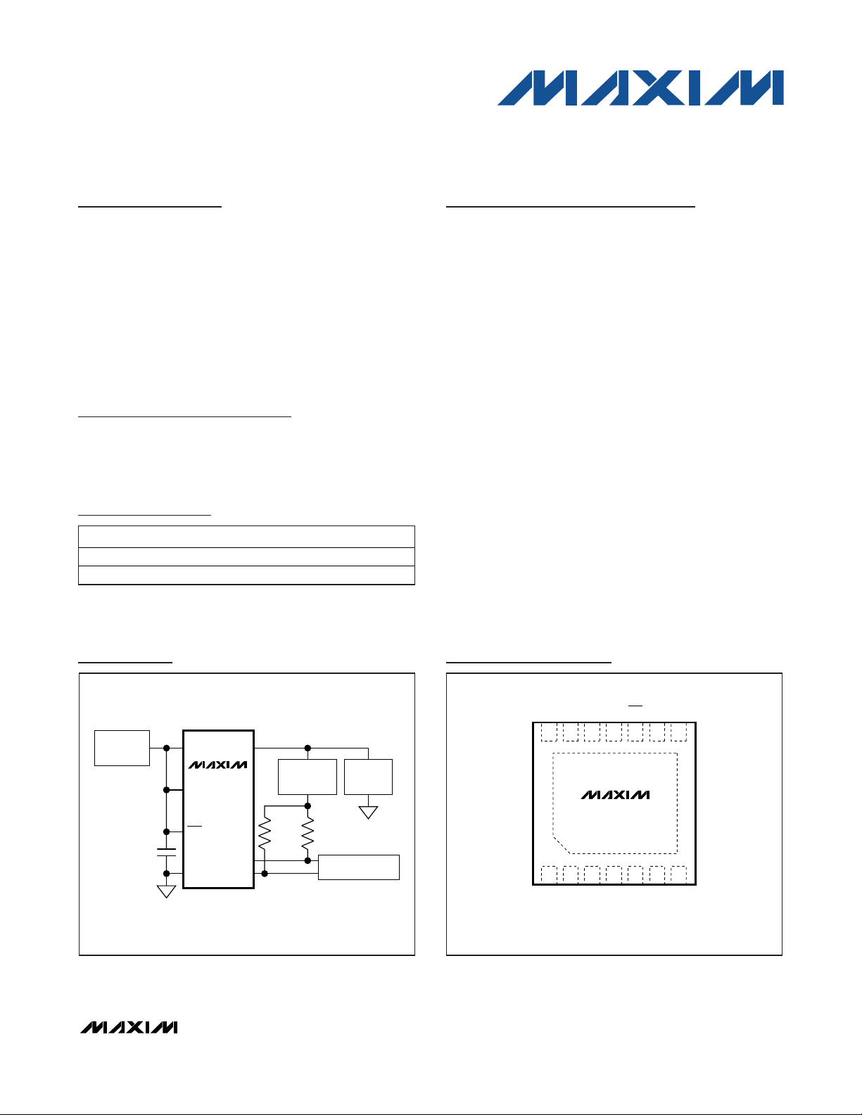
2.2kΩ
1.8V
2.2kΩ
0.1μF
RS+
GND
SLP
V
CC
RS-
SDA
SCL
DC-DC
CONVERTER
Li +
BATTERY
MICROPROCESSOR
CHARGER/
LOAD
Typical Operating Circuit
Rev 0; 8/08
For pricing, delivery, and ordering information, please contact Maxim Direct at 1-888-629-4642,
or visit Maxim’s website at www.maxim-ic.com.
+
Denotes a lead-free/RoHS-compliant package.
T = Tape and reel.
*
EP = Exposed pad.
PART TEMP RANGE PIN-PACKAGE
DS2741N+ -20°C to +70°C 14 TDFN-EP*
DS2741N+T -20°C to +70°C 14 TDFN-EP*
RS-
12
DS2741
245
3
RS+
TDFN
GND
SCL
DNC
9
8
EP*
6
7
V
CC
TOP VIEW
*EXPOSED PAD
RS- RS- SLP
RS-
13 11 10
14
+
1
RS+ RS+ SDA
RS+
Page 2
DS2741
Current Monitor and Accumulator with
Integrated Sense Resistor
2 _______________________________________________________________________________________
ABSOLUTE MAXIMUM RATINGS
RECOMMENDED OPERATING CONDITIONS
(TA= -20°C to +70°C.)
Stresses beyond those listed under “Absolute Maximum Ratings” may cause permanent damage to the device. These are stress ratings only, and functional
operation of the device at these or any other conditions beyond those indicated in the operational sections of the specifications is not implied. Exposure to
absolute maximum rating conditions for extended periods may affect device reliability.
Voltage Range on VCCRelative to GND ...............-0.5V to +6.0V
Voltage Range on SDA, SCL,
RS+, RS-, SLP Relative to GND.....-0.5V to (V
CC
+ 0.5V), not to
exceed +6.0V
Continuous Internal Sense Resistor Current ......................±2.7A
Pulsed Internal Sense Resistor
Current ..................................±10A for <100µs/s, <1000 pulses
Operating Temperature Range ...........................-20°C to +70°C
Storage Temperature Range .............................-55°C to +125°C
Soldering Temperature...........................Refer to the IPC/JEDEC
J-STD-020 Specification.
DC ELECTRICAL CHARACTERISTICS
(2.5V ≤ VCC≤ 4.5V, TA= -20°C to +70°C.)
Supply Voltage VCC (Note 1) 2.5 4.5 V
Input Logic-High: SCL, SDA VIH 1.5 V
Input Logic-Low: SCL, SDA VIL 0.4 V
Input Logic-High: SLP V
Input Logic-Low: SLP V
Power-Up Ramp Time from
0V to V
PARAMETER SYMBOL CONDITIONS MIN TYP MAX UNITS
IH
IL
t
25 ms
CCMI N
RAMP
0.7 x
V
CC
V
0.3 x
V
CC
V
Active Current I
Sleep-Mode Current I
Output Logic-Low: SDA VOL IOL = 4mA (Note 1) 0.4 V
Internal Current-Sense Re sis tor
Value
Current Resolution I
Current Ful l-Scale Magnitude IFS (Note 2) 2.54 2.7 A
Current-Sense Accuracy at +25°C ATL I
Current-Sense Accuracy from
0°C to +70°C
Current Sampling Rate t
Accumulator Resolution qCA 0.247 mAh
Internal Time-Base Accuracy
Current-Sense Offset Mea sured w ith RS+ and RS- shorted -10 +10 mA
PARAMETER SYMBOL CONDITIONS MIN TYP MAX UNITS
ACTIVE
SLEEP
R
SNS
LSB
A
TL
CSR
t
ERR1
t
ERR2
SLP = SCL = SDA = VCC 60 90 μA
SLP = 0V 1 2 μA
+25°C 38 45 m
2.64 mA
at 1.5A ±1 ±2 %
SENSE
I
(Note 3) 200 μs
(Note 4) ±1 ±3
(Note 4) ±6.5
at 1.5A ±2 ±4 %
SENSE
%
Page 3
DS2741
Current Monitor and Accumulator with
Integrated Sense Resistor
_______________________________________________________________________________________ 3
TEMPERATURE SENSOR CHARACTERISTICS
(VCC= +2.5V to +4.5V, TA= -20°C to +70°C, unless otherwise noted.)
AC ELECTRICAL CHARACTERISTICS: I2C INTERFACE
(2.5V ≤ VCC≤ 4.5V, TA= -20°C to +70°C, timing referenced to V
IL(MAX)
and V
IH(MIN)
. See Figure 4.)
Note 1: All voltages are referenced to GND. Currents entering the IC are specified positive and currents exiting the IC are negative.
Note 2: Compensation of the internal sense resistor value for initial tolerance and temperature coefficient of -20°C to +70°C can
reduce the maximum reportable magnitude to 2.5A.
Note 3: Current sampling ceases for 2.5ms every 144ms to allow the ADC to measure temperature.
Note 4: Typical value for t
ERR1
is specified at 3.6V and +25°C, max value is specified for 0°C to +50°C. Max value for t
ERR2
is
specified for -20°C to +70°C.
Note 5: Interface timing shown is for fast-mode (400kHz) operation. This device is also backward compatible with standard-mode
I
2
C timing.
Note 6: C
B
—Total capacitance of one bus line in pF; timing referenced to 0.1 x VCCand 0.9 x VCC.
Temperature Error ±5 °C
PARAMETER SYMBOL CONDITIONS MIN TYP MAX UNITS
SCL Clock Frequenc y f
Bus Free Time Between STOP
and START Conditions
Hold Time (Repeated) START
Condition
Low Period of SCL t
High Period of SCL t
Data Hold Time t
Data Setup Time t
START Setup Time t
SDA a nd SCL R i se Time tR (Note 6)
SDA and SCL Fall Time tF (Note 6)
STOP Setup Time t
SDA a nd SCL Capacit i ve
Loading
PARAMETER SYMBOL CONDITIONS MIN TYP MAX UNITS
(Note 5) 0 400 kHz
SCL
t
1.3 μs
BUF
t
0.6 μs
HD:STA
1.3 μs
LOW
0.6 μs
HIGH
0 0.9 μs
HD:DAT
100 ns
SU:DAT
0.6 μs
SU:STA
0.6 μs
SU:STO
(Note 6) 400 pF
C
B
0.1C
0.1C
20 +
20 +
B
B
300 ns
300 ns
Page 4

DS2741
Current Monitor and Accumulator with
Integrated Sense Resistor
4 _______________________________________________________________________________________
Typical Operating Characteristics
(VCC= +2.5V to +4.5V, TA= -20°C to +70°C, unless otherwise noted.)
70
SLP = SDA = SCL = V
TA = +25°C
60
50
40
30
SUPPLY CURRENT (μA)
20
10
0
2.5 4.5
70
SLP = SDA = SCL = VCC = +3.5V
= +25°C
T
A
60
50
40
30
SUPPLY CURRENT (μA)
20
10
0
0 400
SUPPLY CURRENT
vs. SUPPLY VOLTAGE
CC
SUPPLY VOLTAGE (V)
SUPPLY CURRENT
vs. SCL FREQUENCY
SCL FREQUENCY (kHz)
SLEEP-MODE CURRENT
vs. SUPPLY VOLTAGE
2.0
SDA = SCL = V
DS2741 toc01
4.03.53.0
SLP = GND
= +25°C
T
A
1.5
1.0
0.5
SLEEP-MODE CURRENT (μA)
0
2.5 4.5
CC
4.03.53.0
SUPPLY VOLTAGE (V)
DS2741 toc02
70
60
50
40
30
SUPPLY CURRENT (μA)
20
10
0
-20 70
DISTRIBUTION OF CURRENT-SENSE
OFFSET
90
80
DS2741 toc04
70
60
50
40
30
POPULATION OF PARTS
20
10
0
35030025020015010050
-10
CURRENT-SENSE OFFSET (mA)
-1 2 5 8-7 -4
247 SAMPLES
60
DS2741 toc05
50
40
30
20
POPULATION OF PARTS
10
0
-2.0
SUPPLY CURRENT
vs. TEMPERATURE
SLP = SDA = SCL = V
= +3.5V
CC
TEMPERATURE (°C)
605040302010-10 0
INITIAL CURRENT-SENSE ACCURACY
DISTRIBUTION
I
AT 1.5A
SENSE
247 SAMPLES
1.61.00.4-0.2-0.8-1.4
CURRENT-SENSE ACCURACY (%)
DS2741 toc03
DS2741 toc06
Page 5

DS2741
Current Monitor and Accumulator with
Integrated Sense Resistor
_______________________________________________________________________________________ 5
Pin Description
Block Diagram
PIN NAME FUNCTION
1–4 RS+
5 SDA
6 SCL Serial Clock Input. SCL is used to synchronize data movement on the I2C serial interface.
7 V
8 DNC Do Not Connect
9 GND Ground
10 SLP
11–14 RS-
— EP Exposed Pad. Can be left floating.
CC
Sense Resistor High Side. Connection to high side of internal 38m sense resistor. All RS+ pins
must be connected together.
2
Serial Data Input/Output. SDA i s the input/output pin for the I
open-drain output and requires an external pullup resi stor.
Supply Voltage. Power-supply input.
Sleep Input (Active Low). When taken low, the DS2741 is placed in a low-power sleep state where
all internal circuitry including the I
resets the device and the I
Sense Resistor Low Side. Connection to low side of internal 38m sense resistor. All RS- pins
must be connected together.
2
2
C bus is disabled. Toggling the SLP pin low and then back h igh
C bus logic.
C seria l interface. The SDA pin is an
V
CC
SLP
SDA
SCL
CURRENT ACCUMULATOR
GND
2
I
C
INTERFACE
CURRENT REGISTER
REGISTER
TEMPERATURE
REGISTER
VOLTAGE
REFERENCE
10-BIT PLUS SIGN
A/D CONVERTER
38mΩ
RS+ RS-
POWER
CONTOL
DS2741
Page 6

DS2741
Detailed Description
The DS2741 is a small, low-cost, current-sensing and
accumulation IC that is intended for current-monitoring
applications. The differential voltage measured across
the on-chip 38mΩ sense resistor is digitized by an
internal ADC that provides an accurately scaled digital
signed 10-bit value that represents bidirectional current
up to ±2.5A. The measured current result is reported in
an internal SRAM register that can be read using the
I2C interface. After each current measurement, the
signed result value is added to an accumulator in order
to maintain a signed accumulated current value with a
0.247mAhr LSB and a full-scale range of ±8.1Ahrs. The
device can be placed into a low-power sleep mode
when current measurements are not needed.
Power Modes
The DS2741 has two power modes: active and sleep.
While in active mode, the DS2741 continually measures
and accumulates current and provides data to the host
system through its I2C interface. In sleep mode, the
DS2741 ceases these activities. The DS2741 enters
sleep mode whenever an active-low signal is applied to
the SLP pin and remains in sleep as long as the SLP
pin is held low. Active mode resumes when the SLP pin
is returned to a logic-high level. The SLP pin resets the
Current and Temperature registers, but not the Current
Accumulator register.
Current Measurement
In active mode, the DS2741 continually measures the current flow into and out of the battery by measuring the voltage drop across the internally integrated 38mΩ
current-sense resistor. The DS2741 considers the voltage
difference between pins RS+ and RS- (VRS= V
RS+
- V
RS-
)
to be the filtered voltage drop across the sense resistor. A positive V
RS
value indicates current is flowing into
the battery (charging), while a negative VRSvalue indicates current is flowing out of the battery (discharging).
VRSis measured with a signed resolution of 10 bits.
The current register is updated in two’s-complement
format every 22.7ms with an average of eight readings.
Current measurements outside the register range are
reported at the range limit. Figure 1 shows the format of
the current register.
The DS2741 maintains the current register in units of
amps, with a resolution of 2.64mA and full-scale range
of no less than ±2.5A. The DS2741 automatically compensates for internal sense resistor process variations
and temperature effects when reporting current.
Current Accumulator
The current accumulator facilitates remaining capacity
estimation by tracking the net current flow into and out of
the battery. Current flow into the battery increments the
current accumulator, while current flow out of the battery
decrements it. The DS2741 maintains the current accumulator 0.247mAhrs resolution and full-scale value of
±8.1Ahrs range. Data is maintained in the current accumulator in two’s-complement format. Figure 2 shows the
format of the current accumulator. The current accumulator is a read/write register that can be altered by the
host system as needed. The Current Accumulator register is not reset when the DS2741 is in sleep mode.
Temperature Measurement
The on-board temperature sensor measures temperatures from +127°C to -128°C. The LSb of register 14h
has a 1°C bit weight. See Figure 3 for the temperature
register’s two’s-complement format.
Current Monitor and Accumulator with
Integrated Sense Resistor
6 _______________________________________________________________________________________
Figure 1. Current Register Format
Figure 2. Current Accumulator Register Format
Figure 3. Temperature Register Format
MSB—ADDRESS 16h LSB—ADDRESS 17h
9
8
7
6
5
4
2
2
2
2
S2
MSb LSb MSb LSb
MSB—ADDRESS 10h LSB—ADDRESS 11h
14
13
12
2
S2
MSb LSb MSb LSb
S2
MSb LSb
6
2
ADDRESS 14h
5
2
2
11
2
4
3
2
2
10
2
2
2
2
3
2
9
8
2
1
2
0
2
2
1
2
2
7
2
2
0
2
XXXXX
6
5
4
3
2
2
2
2
2
1
2
0
2
Page 7

DS2741
Current Monitor and Accumulator with
Integrated Sense Resistor
_______________________________________________________________________________________ 7
Figure 4. I2C Timing Diagram
Registers
The DS2741 has 2-byte registers for current measurement and accumulation. When the MSB of a 2-byte register is read, both the MSB and LSB are latched and
held for the duration of the read data command to prevent updates during the read and ensure synchronization between the two register bytes. For consistent
results, always read the MSB and the LSB of a 2-byte
register during the same read data command sequence.
I2C Bus Interface
I2C Definitions
The following terminology is commonly used to
describe I2C data transfers.
Master Device: The master device controls the slave
devices on the bus. The master device generates
SCL clock pulses and START and STOP conditions.
Slave Devices: Slave devices send and receive
data at the master’s request.
Bus Idle or Not Busy: Time between STOP and
START conditions when both SDA and SCL are inactive and in their logic-high states. When the bus is idle
it often initiates a low-power mode for slave devices.
START Condition: A START condition is generated
by the master to initiate a new data transfer with a
slave. Transitioning SDA from high to low, while SCL
remains high, generates a START condition. See
Figure 4 for applicable timing.
STOP Condition: A STOP condition is generated by
the master to end a data transfer with a slave.
Transitioning SDA from low to high, while SCL
remains high, generates a STOP condition. See
Figure 4 for applicable timing.
Repeated START Condition: The master can use a
repeated START condition at the end of one data
transfer to indicate that it will immediately initiate a
new data transfer following the current one.
Repeated STARTs are commonly used during read
operations to identify a specific memory address to
begin a data transfer. A repeated START condition
is issued identically to a normal START condition.
See Figure 4 for applicable timing.
Bit Write: Transitions of SDA must occur during the
low state of SCL. The data on SDA must remain
valid and unchanged during the entire high pulse of
SCL plus the setup and hold-time requirements (see
Figure 4). Data is shifted into the device during the
rising edge of the SCL.
Table 1. Register Map
ADDRESS
(HEX)
00h to 0Fh Reserved —
10h and 11h Current Accumulator Register R/W
12h and 13h Reserved —
14h Temperature Register R
15h Re served —
16h and 17h Current Register R
18h to FFh Re served —
DESCRIPTION READ/WRITE
SDA
t
BUF
SCL
t
HD:STA
STOP START REPEATED
NOTE: TIMING IS REFERENCED TO V
IL(MAX)
t
LOW
AND V
IH(MIN)
t
F
t
t
R
t
HD:DAT
.
HIGH
t
SU:DAT
START
t
SU:STA
t
HD:STA
t
SP
t
SU:STO
Page 8

DS2741
Current Monitor and Accumulator with
Integrated Sense Resistor
8 _______________________________________________________________________________________
Bit Read: At the end a write operation, the master
must release the SDA bus line for the proper amount
of setup time (Figure 4) before the next rising edge
of SCL during a bit read. The device shifts out each
bit of data on SDA at the falling edge of the previous
SCL pulse, and the data bit is valid at the rising
edge of the current SCL pulse. Remember that the
master generates all SCL clock pulses, including
when it is reading bits from the slave.
Acknowledgement (ACK and NACK): An acknowledgement (ACK) or not acknowledge (NACK) is
always the 9th bit transmitted during a byte transfer.
The device receiving data (the master during a read
or the slave during a write operation) performs an
ACK by transmitting a zero during the 9th bit. A
device performs a NACK by transmitting a one during the 9th bit. Timing for the ACK and NACK is
identical to all other bit writes (see Figure 4). An
ACK is the acknowledgment that the device is properly receiving data. A NACK is used to terminate a
read sequence or as an indication that the device is
not receiving data.
Byte Write: A byte write consists of 8 bits of information transferred from the master to the slave
(most significant bit first) plus a 1-bit acknowledgement from the slave to the master. The 8 bits transmitted by the master are done according to the
bit-write definition and the acknowledgement is read
using the bit-read definition.
Byte Read: A byte read is an 8-bit information transfer from the slave to the master plus a 1-bit ACK or
NACK from the master to the slave. The 8 bits of
information that are transferred (most significant bit
first) from the slave to the master are read by the
master using the bit-read definition, and the master
transmits an ACK using the bit-write definition to
receive additional data bytes. The master must
NACK the last byte read to terminate communication
so that the slave returns control of SDA to the master.
Slave Address Byte: Each slave on the I2C bus
responds to a slave addressing byte sent immediately following a START condition. The slave
address byte (Figure 5) contains the slave address
in the most significant 7 bits and the R/W bit in the
least significant bit.
The DS2741’s default factory programmed 7-bit
slave address is 0110100b (binary) or 68h (hex). By
writing the correct slave address with R/W = 0, the
master indicates it will write data to the slave. If
R/W = 1, the master reads data from the slave. If an
incorrect slave address is written, the DS2741
assumes the master is communicating with another
I
2
C device and ignores the communications until the
next start condition is sent. This value can be
changed at the factory to match the user’s need.
Contact the factory for more details on custom I2C
device addresses for the DS2741.
Memory Address: During an I2C write operation,
the master must transmit a memory address to identify the memory location where the slave is to store
the data. The memory address is always the second
byte transmitted during a write operation following
the slave address byte.
I2C Communication
See Figure 6 for examples of I2C communication.
Writing a Single Byte to a Slave: The master must
generate a START condition, write the slave address
byte (R/W = 0), write the memory address, write the
byte of data, and generate a STOP condition.
Remember that the master must read the slave’s
acknowledgement during all byte-write operations.
Writing Multiple Bytes to a Slave: To write multiple
bytes to a slave, the master generates a START condition, writes the slave address byte (R/W = 0),
writes the memory address, writes up to 8 data
bytes, and generates a STOP condition.
Reading a Single Byte from a Slave: Unlike the
write operation that uses the memory address byte
to define where the data is to be written, the read
operation occurs at the present value of the memory
address counter. To read a single byte from the
slave the master generates a START condition,
writes the slave address byte with R/W = 1, reads
the data byte with a NACK to indicate the end of the
transfer, and generates a STOP condition.
Manipulating the Address Counter for Reads: A
dummy write cycle can be used to force the address
counter to a particular value. To do this the master
generates a START condition, writes the slave
address byte (R/W = 0), writes the memory address
where it desires to read, generates a repeated
START condition, writes the slave address byte
(R/W = 1), reads data with ACK or NACK as applica-
Figure 5. DS2741 Slave Address Byte
7-BIT SLAVE ADDRESS
10 1 R/W0100
MOST
SIGNIFICANT BIT
DETERMINES
READ OR WRITE
Page 9

DS2741
Current Monitor and Accumulator with
Integrated Sense Resistor
Maxim cannot assume responsibility for use of any circuitry other than circuitry entirely embodied in a Maxim product. No circuit patent licenses are
implied. Maxim reserves the right to change the circuitry and specifications without notice at any time.
Maxim Integrated Products, 120 San Gabriel Drive, Sunnyvale, CA 94086 408-737-7600 _____________________
9
© 2008 Maxim Integrated Products is a registered trademark of Maxim Integrated Products, Inc.
DS2741
ble, and generates a STOP condition. See Figure 6
for a read example using the repeated START condition to specify the starting memory location.
Reading Multiple Bytes from a Slave: The read
operation can be used to read multiple bytes with a
single transfer. When reading bytes from the slave,
the master simply ACKs the data byte if it desires to
read another byte before terminating the transaction.
After the master reads the last byte, it NACKs to
indicate the end of the transfer and generates a
STOP condition. This can be done with or without
modifying the address counter’s location before the
read cycle. The DS2741’s address counter does not
wrap on page boundaries during read operations,
but the counter rolls from its uppermost memory
address FFh to 00h if the last memory location is
read during the read transaction.
Applications Information
Power-Supply Decoupling
To achieve best results, it is recommended that the power
supply is decoupled with a 0.01µF or a 0.1µF capacitor.
Use high-quality, ceramic, surface-mount capacitors, and
mount the capacitors as close as possible to the VCCand
GND pins to minimize lead inductance.
SDA and SCL Pullup Resistors
SDA is an open-collector output on the DS2741 that
requires a pullup resistor to realize high logic levels. A
master using either an open-collector output with a
pullup resistor or a push-pull output driver can be used
for SCL. Pullup resistor values should be chosen to
ensure that the rise and fall times listed in the AC electrical characteristics are within specification.
Package Information
For the latest package outline information and land patterns, go
to www.maxim-ic.com/packages
.
Figure 6. I2C Communications Examples
PACKAGE TYPE PACKAGE CODE DOCUMENT NO.
14 TDFN-EP T1433+2
21-0137
COMMUNICATIONS KEY
S
START
STOP
P
REPEATED
SR
START
WRITE TWO BYTES WITH A SINGLE TRANSACTION TO SLAVE ADRESS 68h
S 0 1 1 0 0 0 A MEMORY ADDRESS A A DATADATA A P01
READ A SINGLE BYTE WITH A DUMMY WRITE CYCLE TO SET THE ADDRESS COUNTER FROM SLAVE ADDRESS 68h
S 0 1 1 0 0 0 A MEMORY ADDRESS01
READ TWO BYTES WITH A DUMMY WRITE CYCLE TO SET THE ADDRESS COUNTER FROM SLAVE ADDRESS 68h
S 0 1 1 0 0 0 A MEMORY ADDRESS01
ACK
A
NACK
N
XXXXXXXX
WHITE BOXES INDICATE THE MASTER IS
CONTROLLING SDA
SHADED BOXES INDICATE THE SLAVE IS
CONTROLLING SDA
8-BIT ADDRESS OR DATA
A DATASR 0 1 1 0 0 1 A
A DATASR 0 1 1 0 0 1 A01
NOTES
01
1) ALL BYTES ARE SENT MOST SIGNIFICANT BIT FIRST.
2) THE FIRST BYTE SENT AFTER A START CONDITION
IS ALWAYS THE SLAVE ADDRESS FOLLOWED BY
THE READ/WRITE BIT.
N
P
A
DATA
N
P
 Loading...