

Page 1

www.maxim-ic.com
m
(
)
O
875
DS2740
High-Precision Coulomb Counter
FEATURES
§ 15-Bit Bidirectional Current Measurement
(DS2740)
§ 1.56mV LSB and ±51.2mV Dynamic
Range
§ 78mA LSB and ±2.56A Dynamic
Range with External 20mW Sense
Resistor (R
§ 156mA LSB and ±5.12A Dynamic
Range with External 10mW Sense
Resistor (R
§ 13-Bit Bidirectional Current Measurement
(DS2740B)
§ 6.25mV LSB and ±51.2mV Dynamic
Range
§ 312mA LSB and ±2.56A Dynamic
Range with External 20mW Sense
Resistor (R
§ 625mA LSB and ±5.12A Dynamic
Range with External 10mW Sense
Resistor (R
§ Analog Input Filter (IS1, IS2) Extends
Dynamic Range for Pulse-Load
Applications
§ Current Accumulation Register
Resolution
§ 6.25mVhr (Both DS2740 and
DS2740B)
§ 0.3125mAhr with External 20mW
R
SNS
§ 0.6250mAhr with External 10mW
R
SNS
§ Dallas 1-Wire® Interface
§ Unique 64-Bit Device Address
§ Standard and Overdrive Timings
(OVD)
§ Low Power Consumption:
§ Active Current: 65mA max
§ Sleep Current: 1mA max
SNS
SNS
SNS
SNS
)
)
)
)
PIN CONFIGURATION
VD
PIO
SNS
1
2
3
4
MAX
DS2740U, DS2740BU
See Table 1 for Ordering Information.
See Table 2 for Detailed Pin Descriptions.
V
DD
DQ
6
V
SS
IS1IS2
PIN DESCRIPTION
OVD- 1-Wire Bus Speed Select
PIO - Programmable I/O Pin
SNS - Sense Resistor Input
IS2 - Current-Sense Input
IS1 - Current-Sense Input
VSS- Device Ground, Current-Sense Resistor
Return
DQ - Data Input/Output
VDD- Power-Supply Input (2.7V to 5.5V)
1-Wire is a registered trademark of Dallas Semiconductor.
1 of 15 033103
Page 2
DS2740
A
Table 1. ORDERING INFORMATION
PART MARKING PIN-PACKAGE
DS2740U
DS2740U/T&R
DS2740BU
DS2740BU/T&R
DS2740
DS2740
DS2740B
DS2740B
15-Bit Current Resolution, mMAX
15-Bit Current Resolution, mMAX, Tape-and-Reel
13-Bit Current Resolution, mMAX
13-Bit Current Resolution, mMAX, Tape-and-Reel
DESCRIPTION
The DS2740 provides high-precision current-flow measurement data to support battery-capacity
monitoring in cost-sensitive applications. Current is measured bidirectionally over a dynamic range of 15
bits (DS2740U) or 13 bits (DS2740UB), with the net flow accumulated in a separate 16-bit register.
Through its 1-Wire interface, the DS2740 allows the host system read/write access to status and current
measurement registers. Each device has a unique factory-programmed 64-bit net address that allows it to
be individually addressed by the host system, supporting multibattery slot operation. The interface can be
operated with standard or overdrive timing.
Although the DS2740 is primarily intended for location on the host system, it is also suited for mounting
in the battery pack. The DS2740 and FuelPack™ algorithms, along with host measurements of
temperature and voltage, form a complete and accurate solution for estimating remaining capacity.
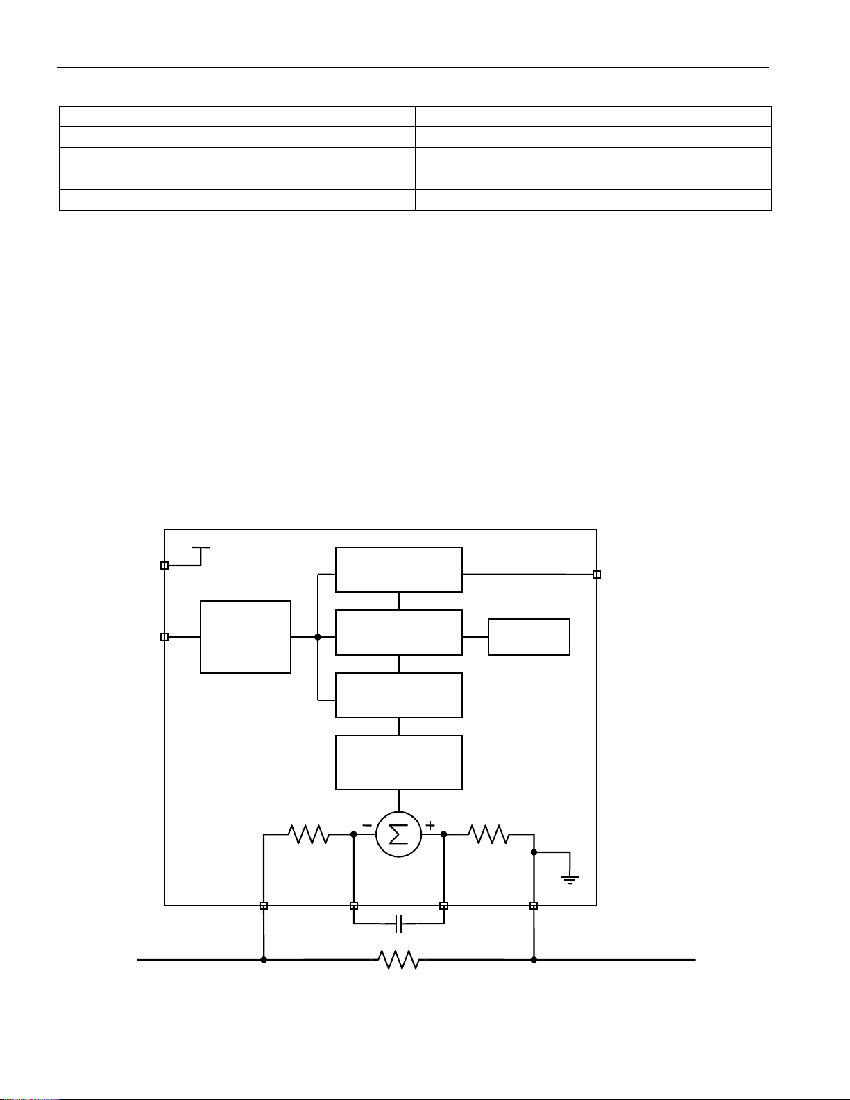
Figure 1. BLOCK DIAGRAM
V
DD
DQ
1-WIRE
INTERFACE
AND
ADDRESS
R
10 k
STATUS/CONTROL
ACCUMULATED
CURRENT
CURRENT
15-Bit + Sign
IS
W
DC
TIMEBASE
R
IS
W
10 k
PIO
CHIP
GROUND
SNS IS2
FuelPack is a trademark of Dallas Semiconductor.
2 of 15
IS1
V
SS
Page 3
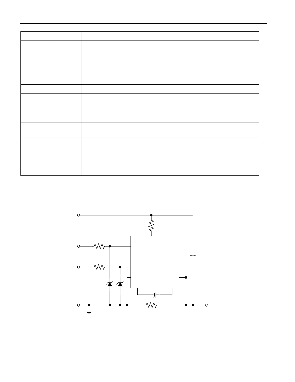
Table 2. DETAILED PIN DESCRIPTION
PIN SYMBOL DESCRIPTION
1-Wire Bus Speed Control. Input logic level selects the speed of the 1-
OVD 1
Wire bus. Logic 1 selects overdrive (OVD) and Logic 0 selects standard
timing (STD). On a multidrop bus, all devices must operate at same
speed.
DS2740
PIO 2
SNS 3
IS2
IS1 5
V
SS
4
6
Programmable I/O Pin. Programmed as input or output through internal
registers. Open-drain output sufficient for LED or vibrator activation.
Current-Sense Resistor Input
Current-Sense Input. Connected to SNS through a 10kΩ resistor to
allow filtering of the current waveform by an external capacitor.
Current-Sense Input. Connected to VSS through a 10kΩ resistor to allow
filtering of the current waveform through an external capacitor.
Device Ground, Current-Sense Resistor Return. Connect directly to
the negative terminal of the battery cell.
Data I/O Pin. Operates bidirectionally with open-drain output driver.
DQ 7
Internal 1µA pulldown aids in sensing pack removal and sleep-mode
activation.
V
DD
8
Power-Supply Input. Connects to system voltage supply or positive
terminal of battery cell.
Figure 2. APPLICATION EXAMPLE
2.7V to 5.5V
System Supply
Battery Pack
150
DATA
PIO
System
150
150
DQ
PIO
SNS
* *
VDD
DS2740
OVD
VSS
IS1IS2
104
GND
R
SNS
* 5.6V zener recommended for ESD protection when DATA or PIO
contacts exposed, such as a removable battery pack application
3 of 15
104
Negative
Battery
Pack
Return
Page 4

DS2740
POWER MODES
The DS2740 has two power modes: active and sleep. While in active mode, the DS2740 operates as a
high-precision coulomb counter with current and accumulated current measurement blocks operating
continuously and the resulting values updated in the measurement registers. Read and write access is
allowed to all registers. PIO pin is active. In sleep mode, the DS2740 operates in a low-power mode with
no current measurement activity. Serial access to current, accumulated current, and status/control
registers is allowed if VDD > 2V.
The DS2740 operating mode transitions from SLEEP to ACTIVE when:
1) DQ > VIH, and VDD > UV threshold, or
2) VDD rises from below UV threshold to above UV threshold.
The DS2740 operating mode transitions from ACTIVE to SLEEP when:
1) VDD falls to UV threshold, or
2) SMOD = 1 and DQ < VIL for 2s.
CURRENT MEASUREMENT
In the active mode of operation, the DS2740 continually measures the current flow into and out of the
battery by measuring the voltage drop across a low-value current-sense resistor, R
range for pulse-type load currents, the voltage signal can be filtered by adding a capacitor between the
IS1 and IS2 pins. The external capacitor and two internal resistors form a lowpass filter at the input of the
ADC. The voltage-sense range at IS1 and IS2 is ±51.2mV. The input converts peak signal amplitudes up
to 75mV as long as the continuous or average signal level (post filter) does not exceed ±51.2mV over the
conversion cycle period. The ADC samples the input differentially at IS1 and IS2 with an 18.6kHz
sample clock and updates the current register at the completion of each conversion cycle. Conversion
times for each resolution option are listed in the tables below. Two resolution options are available.
Figure 3 describes the current measurement register format and resolution for each option. “S” indicates
the sign bit(s).
. To extend the input
SNS
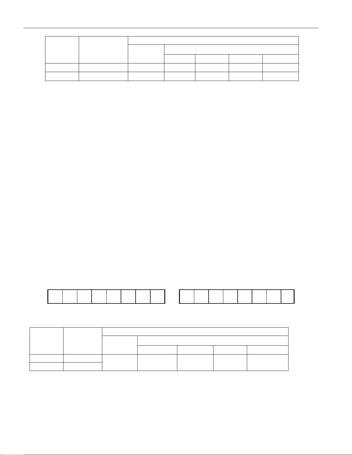
Figure 3. CURRENT REGISTER FORMATS
DS2740: 15-bit + sign resolution, 3.5s conversion period.
MSB—Address 0E LSB—Address 0F
S2142132122112
1029
MSb LSb MSb LSb
DS2740B: 13-bit + sign resolution, 0.875s conversion period.
MSB—Address 0E LSB—Address 0F
SSS2122112
1029
MSb LSb MSb LSb
2
2
8
8
4 of 15
272625242322212
Units: 1.5625mV/Rsns
272625242322212
Units: 6.250mV/Rsns
0
0
Page 5
DS2740
CURRENT RESOLUTION (1 LSB)
PART
DS2740
DS2740B
CONVERSION
TIME
3.515s
0.878s
V
- V
IS1
IS2
20mW 15mW 10mW 5mW
1.5625mV 78.13mA 104.2mA 156.3mA 312.5mA
6.250mV 312.5mA 416.7mA 625mA
R
SNS
1.250mA
Every 1024th conversion, the ADC measures its input offset to facilitate offset correction. Offset
correction occurs approximately once per hour in the DS2740 and four times per hour in the DS2740B.
The resulting correction factor is applied to the subsequent 1023 measurements. During the offset
correction conversion, the ADC does not measure the IS1 to IS2 signal. A maximum error of 1/1024 in
the accumulated current register (ACR) is possible, however, to reduce the error, the current measurement
just prior to the offset conversion is displayed in the current register and is substituted for the dropped
current measurement in the current accumulation process. The typical error due to offset correction is
much less than 1/1024.
CURRENT ACCUMULATOR
Current measurements are internally summed, or accumulated, at the completion of each conversion
period with the results displayed in the ACR. The accuracy of the ACR is dependent on both the current
measurement and the conversion timebase. The ACR has a range of ±204.8mVh with an LSb of
6.25µVh. Additional registers hold fractional results of each accumulation, however, these bits are not
user accessible.
Read and write access is allowed to the ACR. Whenever the ACR is written, fractional accumulation
results are cleared. Also, a write forces the ADC to measure its offset and update the offset correction
factor. The current measurement and accumulation begin with the second conversion following a write to
the ACR. Figure 4 describes the ACR address, format, and resolution.
Figure 4. CURRENT ACCUMULATOR FORMAT
MSB—Address 10 LSB—Address 11
1421321221121029
S2
MSb LSb MSb LSb
PART
DS2740
DS2740B
UPDATE
INTERVAL
3.515s
0.878s
V
- V
IS1
IS2
6.25mVh 312.5mAh 416.7mAh 625mAh
8
2
272625242322212
Units: 6.25mVh/Rsns
ACR LSB
R
SNS
20mW 15mW 10mW 5mW
1.250mAh
0
5 of 15
Page 6

DS2740
ACR RANGE
PART
DS2740
DS2740B
V
- V
IS1
IS2
20mW 15mW 10mW 5mW
±204.8mVh ±10.24Ah ±13.65Ah ±20.48Ah ±40.96Ah
R
SNS
MEMORY
The DS2740 has memory space with registers for instrumentation, status, and control. When the MSB of
a two-byte register is read, both the MSB and LSB are latched and held for the duration of the read data
command to prevent updates during the read and ensure synchronization between the two register bytes.
For consistent results, always read the MSB and the LSB of a two-byte register during the same read data
command sequence.
Table 3. MEMORY MAP
ADDRESS (HEX) DESCRIPTION READ/WRITE
00 Reserved —
01 Status Register R
02 to 07 Reserved —
08 Special Feature Register R/W
09 to 0D Reserved —
0E Current Register MSB R
0F Current Register LSB R
10 Accumulated Current Register MSB R/W
11 Accumulated Current Register LSB R/W
12 to FF Reserved —
STATUS REGISTER
The format of the status register is shown in Figure 5. The function of each bit is described in detail in the
following paragraphs.
Figure 5. STATUS REGISTER FORMAT
ADDRESS 01
BIT 7 BIT 6 BIT 5 BIT 4 BIT 3 BIT 2 BIT 1 BIT 0
X SMOD X RNAOP X X X X
SMOD—SLEEP Mode Enable. A value of 1 allows the DS2740 to enter sleep mode when DQ is low for
2s. A value of 0 disables DQ related transitions to sleep mode. The power-up default of SMOD = 0.
RNAOP—Read Net Address Opcode. A value of 0 in this bit sets the opcode for the read net address
command to 33h, while a 1 sets the opcode to 39h. The power-up default of RNAOP = 0.
X—Reserved bits.
6 of 15
Page 7

DS2740
SPECIAL FEATURE REGISTER
The format of the special feature register is shown in Figure 6. The function of each bit is described in
detail in the following paragraphs.
Figure 6. SPECIAL FEATURE REGISTER FORMAT
ADDRESS 08
BIT 7 BIT 6 BIT 5 BIT 4 BIT 3 BIT 2 BIT 1 BIT 0
X
PIO—PIO Pin Sense and Control. This bit is read and write enabled. Writing a 0 to the PIO bit enables
the PIO open-drain output driver, forcing the PIO pin low. Writing a 1 to the PIO bit disables the output
driver, allowing the PIO pin to be pulled high or used as an input. Reading the PIO bit returns the logic
level forced on the PIO pin. Note that if PIO is left floating, the weak pulldown brings the pin low.
X—Reserved Bits.
PIO X X X X X X
1-WIRE BUS SYSTEM
The 1-Wire bus is a system that has a single bus master and one or more slaves. A multidrop bus is a
1-Wire bus with multiple slaves. A single-drop bus has only one slave device. In all instances, the
DS2740 is a slave device. The bus master is typically a microprocessor in the host system. The discussion
of this bus system consists of four topics: 64-bit net address, hardware configuration, transaction
sequence, and 1-Wire signaling.
64-BIT NET ADDRESS
Each DS2740 has a unique, factory-programmed 1-Wire net address that is 64 bits in length. The first
eight bits are the 1-Wire family code (36h for DS2740). The next 48 bits are a unique serial number. The
last eight bits are a cyclic redundancy check (CRC) of the first 56 bits (see Figure 7). The 64-bit net
address and the 1-Wire I/O circuitry built into the device enable the DS2740 to communicate through the
1-Wire protocol detailed in the 1-Wire Bus System section of this data sheet.
Figure 7. 1-WIRE NET ADDRESS FORMAT
8-BIT CRC 48-BIT SERIAL NUMBER
MSb LSb
8-BIT FAMILY
CODE (36h)
CRC GENERATION
The DS2740 has an 8-bit CRC stored in the most significant byte of its 1-Wire net address. To ensure
error-free transmission of the address, the host system can compute a CRC value from the first 56 bits of
the address and compare it to the CRC from the DS2740. The host system is responsible for verifying the
CRC value and taking action as a result. The DS2740 does not compare CRC values and does not prevent
a command sequence from proceeding as a result of a CRC mismatch. Proper use of the CRC can result
in a communication channel with a very high level of integrity.
The CRC can be generated by the host using a circuit consisting of a shift register and XOR gates as
shown in Figure 8, or it can be generated in software. Additional information about the Dallas 1-Wire
7 of 15
Page 8

DS2740
CRC is available in Application Note 27, Understanding and Using Cyclic Redundancy Checks with
Dallas Semiconductor Touch Memory Products. (This application note can be found on the Maxim/Dallas
Semiconductor website at www.maxim-ic.com.)
In the circuit in Figure 8, the shift register bits are initialized to 0. Then, starting with the least significant
bit of the family code, one bit at a time is shifted in. After the 8th bit of the family code has been entered,
then the serial number is entered. After the 48th bit of the serial number has been entered, the shift
register contains the CRC value.
Figure 8. 1-WIRE CRC GENERATION BLOCK DIAGRAM
INPUT
MSb
XOR XOR
LSb
XOR
HARDWARE CONFIGURATION
Because the 1-Wire bus has only a single line, it is important that each device on the bus be able to drive
it at the appropriate time. To facilitate this, each device attached to the 1-Wire bus must connect to the
bus with open-drain or tri-state output drivers. The DS2740 uses an open-drain output driver as part of the
bidirectional interface circuitry shown in Figure 9. If a bidirectional pin is not available on the bus master,
separate output and input pins can be connected together.
The 1-Wire bus must have a pullup resistor at the bus-master end of the bus. For short line lengths, the
value of this resistor should be approximately 5kW. The idle state for the 1-Wire bus is high. If, for any
reason, a bus transaction must be suspended, the bus must be left in the idle state to properly resume the
transaction later. If the bus is left low for more than 120ms (16ms for overdrive speed), slave devices on
the bus begin to interpret the low period as a reset pulse, effectively terminating the transaction.
The DS2740 can operate in two communication speed modes, standard and overdrive. The speed mode is
determined by the input logic level of the OVD pin with a logic 0 selecting standard speed and a logic 1
selecting overdrive speed. The OVD pin must be at a stable logic level of 0 or 1 before initializing a
transaction with a reset pulse. All 1-Wire devices on a multinode bus must operate at the same
communication speed for proper operation. 1-Wire timing for both standard and overdrive speeds are
listed in the Electrical Characteristics: 1-Wire Interface tables.
8 of 15
Page 9

Figure 9. 1-WIRE BUS INTERFACE CIRCUITRY
DS2740
BUS MASTER DS2740 1-WIRE PORT
Tx
Vpullup
(2.0V to 5.5V)
4.7kW
1mA
(typ)
Rx = RECEIVE
Tx = TRANSMIT
TRANSACTION SEQUENCE
The protocol for accessing the DS2740 through the 1-Wire port is as follows:
§ Initialization
§ Net Address Command
§ Function Command
§ Transaction/Data
RxRx
Tx
100W
MOSFET
The sections that follow describe each of these steps in detail.
All transactions of the 1-Wire bus begin with an initialization sequence consisting of a reset pulse
transmitted by the bus master followed by a presence pulse simultaneously transmitted by the DS2740
and any other slaves on the bus. The presence pulse tells the bus master that one or more devices are on
the bus and ready to operate. For more details, see the 1-Wire Signaling section.
NET ADDRESS COMMANDS
Once the bus master has detected the presence of one or more slaves, it can issue one of the net address
commands described in the following paragraphs. The name of each ROM command is followed by the
8-bit opcode for that command in square brackets. Figure 10 presents a transaction flowchart of the net
address commands.
Read Net Address [33h or 39h]. This command allows the bus master to read the DS2740’s 1-Wire net
address. This command can only be used if there is a single slave on the bus. If more than one slave is
present, a data collision occurs when all slaves try to transmit at the same time (open drain produces a
wired-AND result). The RNAOP bit in the status register selects the opcode for this command, with
RNAOP = 0 indicating 33h, and RNAOP = 1 indicating 39h.
Match Net Address [55h]. This command allows the bus master to specifically address one DS2740 on
the 1-Wire bus. Only the addressed DS2740 responds to any subsequent function command. All other
slave devices ignore the function command and wait for a reset pulse. This command can be used with
one or more slave devices on the bus.
9 of 15
Page 10

DS2740
Skip Net Address [CCh]. This command saves time when there is only one DS2740 on the bus by
allowing the bus master to issue a function command without specifying the address of the slave. If more
than one slave device is present on the bus, a subsequent function command can cause a data collision
when all slaves transmit data at the same time.
Search Net Address [F0h]. This command allows the bus master to use a process of elimination to
identify the 1-Wire net addresses of all slave devices on the bus. The search process involves the
repetition of a simple three-step routine: read a bit, read the complement of the bit, then write the desired
value of that bit. The bus master performs this simple three-step routine on each bit location of the net
address. After one complete pass through all 64 bits, the bus master knows the address of one device. The
remaining devices can then be identified on additional iterations of the process. See Chapter 5 of the Book
of DS19xx iButton® Standards for a comprehensive discussion of a net address search, including an actual
example. (This publication can be found on the Maxim/Dallas Semiconductor website at www.maximic.com.)
Resume [A5h]. This command increases data throughput in multidrop environments where the DS2740
needs to be accessed several times. Resume is similar to the Skip Net Address command in that the 64bit net address does not have to be transmitted each time the DS2740 is accessed. After successfully
executing a Match Net Address command or Search Net Address command, an internal flag is set in the
DS2740. When the flag is set, the DS2740 can be repeatedly accessed through the Resume command
function. Accessing another device on the bus clears the flag, thus preventing two or more devices from
simultaneously responding to the Resume command function.
FUNCTION COMMANDS
After successfully completing one of the net address commands, the bus master can access the features of
the DS2740 with any of the function commands described in the following paragraphs and summarized in
Table 4. The name of each function is followed by the 8-bit opcode for that command in square brackets.
Read Data [69h, XX]. This command reads data from the DS2740 starting at memory address XX. The
LSb of the data in address XX is available to be read immediately after the MSb of the address has been
entered. Because the address is automatically incremented after the MSb of each byte is received, the LSb
of the data at address XX + 1 is available to be read immediately after the MSb of the data at address XX.
If the bus master continues to read beyond address FFh, the DS2740 starts over at address 00h.
Addresses labeled “Reserved” in the memory map contain undefined data. The read data command can be
terminated by the bus master with a reset pulse at any bit boundary.
Write Data [6Ch, XX]. This command writes data to the DS2740 starting at memory address XX. The
LSb of the data to be stored at address XX can be written immediately after the MSb of address has been
entered. Because the address is automatically incremented after the MSb of each byte is written, the LSb
to be stored at address XX + 1 can be written immediately after the MSb to be stored at address XX. If
the bus master continues to write beyond address FFh, the DS2740 starts over writing at address 00h.
Writes to read-only addresses and reserved addresses are ignored. Incomplete bytes are not written. See
the Memory section for more details.
iButton is a registered trademark of Dallas Semiconductor.
10 of 15
Page 11

Figure 10. NET ADDRESS COMMAND FLOW CHART
MASTER Tx
RESET PULSE
DS2740 Tx
PRESENCE PULSE
MASTER Tx NET
ADDRESS
COMMAND
DS2740
33h / 39h
READ
DS2740 Tx
FAMILY CODE
1 BYTE
DS2740 Tx
SERIAL NUMBER
6 BYTES
DS2740 Tx
CRC
1 BYTE
NO NO NO
55h
MATCH
MASTER Tx
BIT 0
BIT 0
MATCH ?
MASTER Tx
BIT 1
BIT 1
MATCH ?
NO NO
NO NO
F0h
SEARCH
YESYESYES
DS2740 Tx BIT 0
DS2740 Tx BIT 0
MASTER Tx BIT 0
BIT 0
MATCH ?
YESYES
DS2740 Tx BIT 1
DS2740 Tx BIT 1
MASTER Tx BIT 1
BIT 1
MATCH ?
YESYES
CCh
SKIP
YES
MASTER Tx
FUNCTION
COMMAND
NO
A5h
RESUME
YES
RESUME
FLAG SET ?
YES
MASTER Tx
FUNCTION
COMMAND
NO
NO
MASTER Tx
FUNCTION
COMMAND
SET
RESUME
FLAG
YES
MASTER Tx
BIT 63
BIT 63
MATCH ?
NO
DS2740 Tx BIT 63
DS2740 Tx BIT 63
MASTER Tx BIT 63
11 of 15
Page 12

DS2740
Table 4. FUNCTION COMMANDS
BUS STATE
AFTER COMMAND
PROTOCOL
BUS DATA
Up to 256 bytes
of data
Up to 256 bytes
of data
COMMAND DESCRIPTION
Reads data from
Read Data
memory starting at
address XX
Write Data
Writes data to memory
starting at address XX
COMMAND
PROTOCOL
69h, XX Master Rx
6Ch, XX Master Tx
1-WIRE SIGNALING
The 1-Wire bus requires strict signaling protocols to ensure data integrity. The four protocols used by the
DS2740 are as follows: the initialization sequence (reset pulse followed by presence pulse), write 0, write
1, and read data. All of these types of signaling except the presence pulse are initiated by the bus master.
The initialization sequence required to begin any communication with the DS2740 is shown in Figure 11.
A presence pulse following a reset pulse indicates that the DS2740 is ready to accept a net address
command. The bus master transmits (Tx) a reset pulse for t
goes into receive mode (Rx). The 1-Wire bus line is then pulled high by the pullup resistor. After
detecting the rising edge on the DQ pin, the DS2740 waits for t
for t
PDL
.
. The bus master then releases the line and
RSTL
and then transmits the presence pulse
PDH
Figure 11. 1-WIRE INITIALIZATION SEQUENCE
DQ
t
RSTL
LINE TYPE LEGEND:
BOTH BUS MASTER AND
DS2740 ACTIVE LOW
t
PDH
t
PDL
t
RSTH
PACK+
PACK-
WRITE-TIME SLOTS
A write-time slot is initiated when the bus master pulls the 1-Wire bus from a logic-high (inactive) level
to a logic-low level. There are two types of write-time slots: write 1 and write 0. All write-time slots must
be t
1-Wire bus line between 15
the line is high when sampled, a write 1 occurs. If the line is low when sampled, a write 0 occurs (see
Figure 12). For the bus master to generate a write 1 time slot, the bus line must be pulled low and then
released, allowing the line to be pulled high within 15
write-time slot. For the host to generate a write 0 time slot, the bus line must be pulled low and held low
for the duration of the write-time slot.
in duration with a 1ms minimum recovery time, t
SLOT
ms and 60ms (between 2ms and 6ms for overdrive speed) after the line falls. If
, between cycles. The DS2740 samples the
REC
ms (2ms for overdrive speed) after the start of the
12 of 15
Page 13

DS2740
X
X
READ-TIME SLOTS
A read-time slot is initiated when the bus master pulls the 1-Wire bus line from a logic-high level to a
logic-low level. The bus master must keep the bus line low for at least 1ms and then release it to allow the
DS2740 to present valid data. The bus master can then sample the data t
from the start of the read-
RDV
time slot. By the end of the read-time slot, the DS2740 releases the bus line and allows it to be pulled
high by the external pullup resistor. All read-time slots must be t
recovery time, t
, between cycles. See Figure 12 for more information.
REC
in duration with a 1ms minimum
SLOT
Figure 12. 1-WIRE WRITE- AND READ-TIME SLOTS
WRITE 0 SLOT WRITE 1 SLOT
t
SLOT
V
PULLUP
GND
t
SLOT
t
LOW0
t
REC
t
LOW1
Mode
Standard
Overdrive
V
PULLUP
GND
DS2740 Sample Window
MIN TYP MA
15ms15ms 30ms
2ms
1ms 3ms 1ms2ms 3ms
READ 0 SLOT
t
SLOT
t
RDV
LINE TYPE LEGEND:
Both bus master and
DS2740 active low
>1ms
>1ms
t
REC
t
RDV
Resistor pullup
DS2740 Sample Window
MIN TYP MA
15ms15ms 30ms
READ 1 SLOT
t
SLOT
13 of 15
Page 14

DS2740
ABSOLUTE MAXIMUM RATINGS*
Voltage on VDD, DQ, IS1, IS2, PIO, Relative to V
Voltage on SNS, Relative to V
SS
SS
Operating Temperature Range -40°C to +85°C
Storage Temperature Range -55°C to +125°C
Soldering Temperature See IPC/JEDECJ-STD-020A
* This is a stress rating only and functional operation of the device at these or any other conditions above
those indicated in the operation sections of this specification is not implied. Exposure to absolute
maximum rating conditions for extended periods of time may affect reliability.
-0.3V to +6V
-0.3V to +6V
RECOMMENDED DC OPERATING CONDITIONS
(2.7V £ V
PARAMETER SYMBOL CONDITIONS MIN TYP MAX UNITS
Supply Voltage V
Data Pin DQ (Note 1) -0.3 +5.5 V
£ 5.5V; TA = 0°C to +70°C.)
DD
DD
(Note 1) 2.7 5.5 V
DC ELECTRICAL CHARACTERISTICS
(2.7V £ V
£ 4.2V; TA = 0°C to +70°C.)
DD
PARAMETER SYMBOL CONDITIONS MIN TYP MAX UNITS
Active Current I
Sleep-Mode Current I
Undervoltage Sleep
Threshold
Current Resolution I
Current Full-Scale
Magnitude
ACTIVE
SLEEP
V
UV
LSB
I
FS
V
= 5.5V 85
DD
V
= 2.0V,
DD
DQ = PIO = V
V
= 4.2V,
DD
DQ = PIO = V
SS
SS
2.3 2.5 2.7 V
DS2740 1.56
DS27640B 6.25
50 65
0.6 1.0
0.9 1.25
51.2
DS2740 (Note 2) -3 +1 +5Current Measurement
Offset (Auto
Calibrated)
Current Gain Error I
Accumulated Current
Resolution
Current Sample Clock
Frequency
Timebase Accuracy t
Input Logic High:
OVD
Input Logic High: DQ,
PIO
Input Logic Low:
OVD
I
OERR
GERR
q
f
SAMP
ERR
V
V
V
CA
IH
IH
IL
DS2740B (Note 2) -2 0 +2
-1 +1
6.25
18.6 kHz
V
= 3.5V at +25°C -1 +1
DD
-4 +4
V
-
(Note 1)
DD
0.2V
(Note 1) 1.5 V
(Note 1)
14 of 15
VSS + 0.2
mA
mA
mV
mV
LSb
% of
reading
mVh
%
V
V
Page 15

Input Logic Low: DQ,
PIO
Output Logic Low:
DQ, PIO
DQ, PIO Input
Pulldown Current
OVD Input Leakage IL
DQ Capacitance C
DQ Low to Sleep Time t
V
IL
V
OL
I
PD
OVD
DQ
SLEEP
(Note 1) 0.6 V
I
= 4mA (Note 1) 0.4 V
OL
V
= 4.2V,
DD
= 0.4V
V
DQ
PIO bit = 1
-1 1
0.5
50 pF
(Note 3) 2.0 2.4 s
ELECTRICAL CHARACTERISTICS: 1-WIRE INTERFACE—STANDARD
SPEED
DS2740
mA
mA
(2.7V £ V
£ 5.5V; TA = -20°C to +70°C.)
DD
PARAMETER SYMBOL MIN TYP MAX UNITS
Time Slot t
Recovery Time t
Write 0 Low Time t
Write 1 Low Time t
Read Data Valid t
Reset Time High t
Reset Time Low t
Presence Detect High t
Presence Detect Low t
SLOT
REC
LOW0
LOW1
RDV
RSTH
RSTL
PDH
PDL
60 120 ms
1 ms
60 120 ms
115ms
15 ms
480 ms
480 960 ms
15 60 ms
60 240 ms
ELECTRICAL CHARACTERISTICS: 1-WIRE INTERFACE—OVERDRIVE
SPEED
(2.7V £ V
Time Slot t
Recovery Time t
Write 0 Low Time t
Write 1 Low Time t
Read Data Valid t
Reset Time High t
Reset Time Low t
Presence Detect High t
Presence Detect Low t
£ 5.5V; TA = -20°C to +70°C.)
DD
PARAMETER SYMBOL MIN TYP MAX UNITS
SLOT
REC
LOW0
LOW1
RDV
RSTH
RSTL
PDH
PDL
616ms
1 ms
616ms
12ms
2 ms
48 ms
48 80 ms
26ms
824ms
Note 1:
Note 2:
Note 3:
All voltages are referenced to V
SS
.
Offset performance requires proper circuit layout design free of surface contaminants.
The DS2740 enters the sleep mode 2.0s to 2.4s after DQ goes low.
15 of 15
 Loading...