

Page 1
r
NiMH Battery Pack Charge Controlle
DS2715
www.maxim-ic.com
DESCRIPTION
The DS2715 is well suited for cost-sensitive charger
applications where the battery is either internal or in a
unique battery pack. It has been optimized for safe
reliable charging of 1 to10 NiMH cells in series. The
DS2715 has an internal gain block that can be
selected as either a comparator or transconductance
amplifier for charge current regulation. The DS2715 is
configurable as a switched DC charger, a linear
current regulator, or a switchmode current source.
The DS2715 pre-conditions severely depleted cells
are pre-conditioned before entering full charge mode.
The DS2715 terminates full charge using the dT/dt
technique. It requires an external thermistor for dT/dt
detection. Over-temperature, under-temperature, and
over-voltage detection prevents charging under
unsafe environmental conditions. A user selectable
charge timer allows charge rates from 0.15C to 2C.
Fast-charge, top-off and charge done modes are
included for highly reliable, safe charging of NiMH
cells. Discharge mode allows the DS2715 to enter a
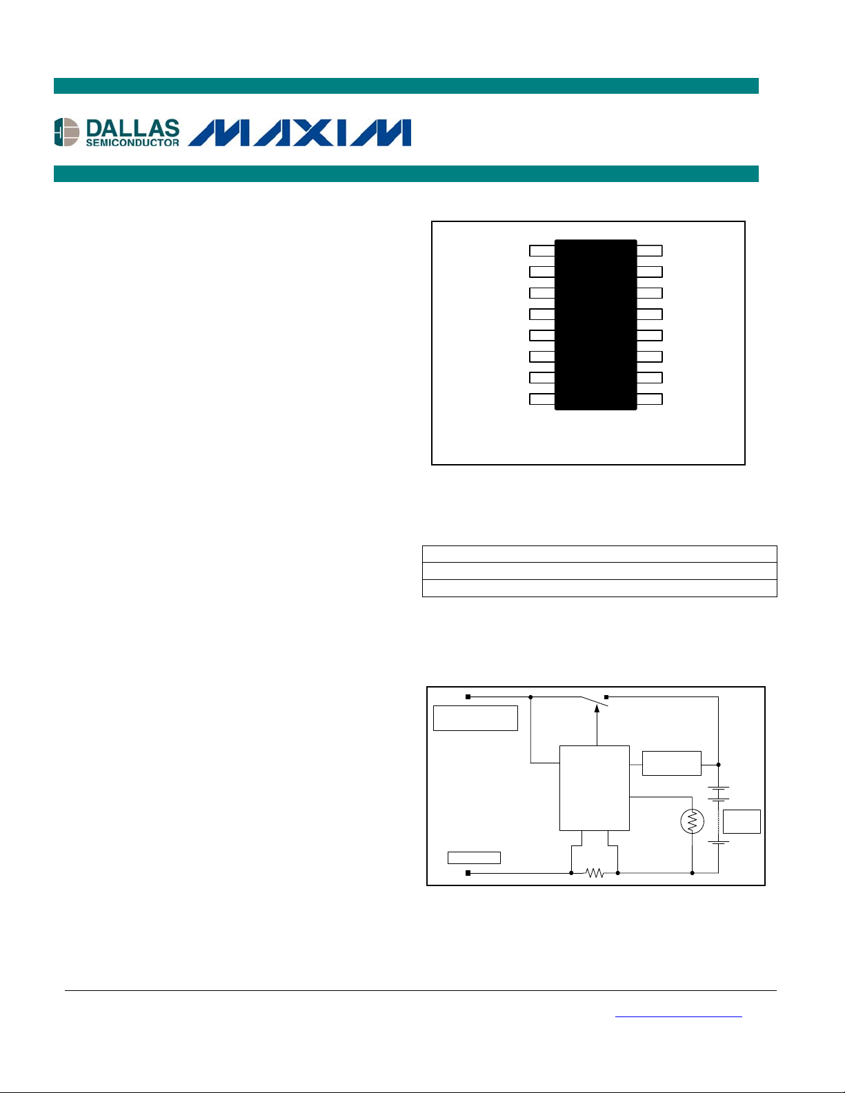
PIN CONFIGURATION
C
CC1
CC2
LED1
LED1
VSS
LED2
LED2
CSOUT
CTG
VN1
CTG
VN0
See Table 1 for Ordering Information.
Table 1.
V
BIAS
V
V
V
CH
1
2
SS
SS
3
4
5
6
7
8
16
15
14
13
12
11
10
9
BATT
VP2
THM
VP1
RT
THM2
V
DD
THM1
SNS-
VDD
SNS+
TMR
DIV
CTST
MODE
DMSEL
16 SO
ORDERING INFORMATION
low power sleep state while the cell pack is being
discharged.
FEATURES
§ Charges 1 to 10 NiMH Cells
§ Fast Charges up to a 2C Rate
§ Pre-Charge and Top-Off Charge Modes Help Cell
Conditioning
§ Load Detection Allows the DS2715 to Enter Low
Power Sleep Mode (Less than 10µA) while the
Cell Pack is Discharged
PART MARKING PIN-PACKAGE
DS2715Z+
DS2715+
16 SO
DS2715Z+T&R DS2715+ 16 SO Tape-and-Reel
+ Denotes lead-free package.
OPERATIONAL DIAGRAM
CHARGE
SOURCE/LOAD
§ dT/dt Charge Termination Eliminates Cell Charge
Stress
§ Monitors Voltage, Temperature, and Time for
Safety and Secondary Termination
§ Regulates Current through Either Linear Control
or Switch-Mode Control
Vdd
Vch
DS2715
+
-
Vbatt
THM
Divide by n
n Cells
§ LED Outputs Display Charge State
§ Small 16-Pin SO Package
GROUND
Sense
APPLICATIONS
Portable DVD Players
Portable Television Sets
Handheld Gaming
Test Equipment
Handheld POS Terminals
Note: Some revisions of this device may incorporate deviations from published specifications known as errata. Multiple revisions of any device
may be simultaneously available through various sales channels. For information about device errata, click here: www.maxim-ic.com/errata.
1 of 12 042605
Page 2
DS2715: NiMH Cell Pack Charge Controller
ABSOLUTE MAXIMUM RATINGS*
Voltage on VDD and VCH Pins with Respect to VSS -0.3V to +18V
Voltage on LED1 and LED2 Pins -0.3V to +18V
Voltage on SNS- -0.3V to +0.3V
Voltage on C
Voltage on all Other Pins -0.3V to V
-0.3V to 6V
BIAS
Cbias
Continuous Sink Current VCH, LED1, and LED2 28mA
Operating Temperature Range -20°C to +85°C
Storage Temperature Range -55°C to +125°C
Soldering Temperature See IPC/JEDECJ-STD-020
*This is a stress rating only and functional operation of the device at these or any other conditions above those indicated in the operation
sections of this specification is not implied. Exposure to absolute maximum rating conditions for extended periods of time may affect reliability.
RECOMMENDED DC OPERATING CONDITIONS
(4.5V £ VDD £ 16.5V; TA = 0°C to +70°C.)
PARAMETER SYMBOL CONDITIONS MIN TYP MAX UNITS
Supply Voltage VDD (Note 1) 4.5 16.5 V
LED1, LED2 Voltage V
Mode Voltage V
VCH Voltage V
C
Capacitor Range C
BIAS
(Note 1) 0.0 16.5 V
LED
(Note 1) 0.0 V
MODE
(Note 1) 0.0 16.5 V
VCH
.02 .15 µF
Cbias
V
Cbias
RT Resistor Range RRt 20 240 KΩ
DC ELECTRICAL CHARACTERISTICS
(4.5V £ VDD £ 16.5V, TA = 0°C to +70°C, unless otherwise noted.)
PARAMETER SYMBOL CONDITIONS MIN TYP MAX UNITS
Operating Current
(Note 2)
Idle Current I
Discharge Current I
UVLO Threshold V
UVLO Hysteresis V
VCH Sink Current I
LED1, LED2 Sink Current I
Leakage Current, VCH,
LED1, LED2
THM Pin Leakage
Current
V
Pin Leakage
BATT
Current
I
I
Linear Mode, V
I
DDA
DDS
DDD
UVLO
UVLO-HYS
OL-Vch
OL-LED
I
LKG
LKG-THM
LKG-Vbatt
Comparator Mode,
V
= 16.5V
DD
VDD < V
UVLO
Discharge latch set (Note 2) 200 µA
VDD Rising (Note 3) 3.8 3.9 4.0 V
VDD Falling 35 mV
VOL = 1.5V 20 mA
VOL = 1.0V 20 mA
Pin inactive or Device Idle -1 +1 µA
-1 +1 µA
-50 +50 nA
= 16.5V 1.3 1.6 mA
DD
150 250 µA
10 µA
C
Voltage V
BIAS
DIV Pin Load Current I
Current Sense Amplifier
Gain
Current Sense
Comparator Gain
0 < I
Cbias
500 uA
Div
G
100µA < I
ERR
G
(Note 7) 10 Ω
COMP
< 0.4ma 3.9 4.0 4.3 V
Cbias
< 20mA 5 6.25 7.5 Ω
Vch
-1
-1
2 of 12
Page 3
DS2715: NiMH Cell Pack Charge Controller
AC ELECTRICAL CHARACTERISTICS
(4.5V £ VDD £ 16.5V, TA = 0°C to +70°C, unless otherwise noted.)
PARAMETER SYMBOL CONDITIONS MIN TYP MAX UNITS
UVLO Debounce Time t
10 µs
UVLO
Current Sense
Comparator Propagation
t
(Note 7) 250 ns
COMP
Delay
Discharge Detect
Propagation Delay
Return To Normal
Function (Op-Amp or
Comparator Mode)
t
t
DD
RNF
From detection of current
reversal
Time from reset of
discharge latch
1 µs
1 µs
RT Timing Accuracy tRt (Note 4) -10 +10 %
Internal Clock Accuracy t
-10 +10 %
BASE
ELECTRICAL CHARACTERISTICS: CHARGING
(4.5V £ VDD £ 16.5V, TA = 0°C to +70°C, unless otherwise noted.)
PARAMETER SYMBOL CONDITIONS MIN TYP MAX UNITS
Fast Charge Comparator
Threshold
Fast Charge Comparator
Hysteresis
Top-off and Pre-Charge
Comparator Threshold
Top-off and Pre-Charge
Comparator Hysteresis
Discharge Latch Reset
Threshold
Discharge Latch Set
Threshold
Low Battery Detect
Threshold
V
Fast charge -127 -121 -115 mV
FC
V
V
V
V
Fast charge -31 -28 -25 mV
HYS-FC
V
Top-off and pre-charge -38 -33 -28 mV
TO
Top-off and pre-charge -10 -8 -6 mV
HYS-TO
DCHG-RST
DCHG-SET
-15 -10 -5 mV
Reverse current through
sense resistor
V
LB
From presence detect into
pre-charge
5 10 15 mV
0.95 1.0 1.05 V
Cell Detect Threshold V
No Cell Detect Threshold V
Presence Detect
Threshold Hysteresis
Minimum Charge Temp V
Maximum Charge Temp V
Over Temp V
dT/dt Detect T
dT/dt Blanking Time t
Fast Charge Timer
Range
Top-Off to Fast Charge
Duration Ratio
1.50 1.55 1.60 V
DET
1.60 1.65 1.70 V
OPEN
V
90 100 110 mV
HYS-PD
(Note 5, 6)
THM-MIN
THM-MAX
THM-STOP
(Note 5, 6)
(Note 5, 6)
0.425 0.5 0.575 ºC/min
TERM
3.85 4.3 4.75 Min
BLANK
t
0.5 6 Hours
FC
1:2
3 of 12
2.88 2.92 2.96 V
0 ºC
1.28 1.32 1.36 V
45 ºC
1.12 1.16 1.20 V
50 ºC
Page 4
DS2715: NiMH Cell Pack Charge Controller
Note 1:
Note 2:
Note 3:
Note 4:
Note 5:
Note 6:
Note 7:
Voltages relative to V
Does not include current through V
Below this voltage no I/O pins are active.
Does not include tolerance of R
V
and resistor tolerances must be added to determine actual threshold.
BIAS
Specified temperature thresholds are only valid if recommended thermistor types are used.
Specification is guaranteed by design.
.
SS
, RT, and DIV pins.
CH
resistor.
T
DETAILED PIN DESCRIPTION
PIN NAME DESCRIPTION
1 C
2 VCH Cell Stack Charge Control Output
3 VSS Ground Reference and Chip Supply Return
4 LED1 Charging Indicator Output
5 LED2 Done Indicator Output
6 VSS Ground Reference and Chip Supply Return
7 CTG Connect to Ground
8 CTG Connect to Ground
9 MODE
10 DIV
11 SNS+ Positive Current Sense. Connect to the pack side of the sense resistor.
12 SNS- Negative Current Sense. Connect to the cell stack side of the sense resistor.
13 VDD Chip Supply Input: +4.0V to +5.5V range.
14 RT Failsafe Timeout. Timeout is selected by an external resistor from RT to VSS.
15 THM
16 V
Bypass for Internal Voltage Regulator
BIAS
Mode Select. Connect to V
for linear mode of operation or C
SS
mode of operation.
Thermistor Divider. Stable output to form a resistor divider for measuring
temperature on THM.
Thermistor Input. Connect to a thermistor located in the cell pack and a divider
resistor from the Div pin.
Battery Voltage Sense Input. Connect to a divider from the positive terminal of the
BATT
cell stack to measure the voltage of a single cell.
for comparator
BIAS
4 of 12
Page 5

Figure 1. BLOCK DIAGRAM
DS2715: NiMH Cell Pack Charge Controller
DS2715
Cbias
VDD
Div
LED1
LED2
Rt
HV
HV
HV
Pwr
Rt
V
UVLO
Disable during
discharge
Oscillator
Rt start-up test
Charge
Timer
Regulator
UVLO
State Machine
Pre-Charge
Low Cells
Fast Charge
Exit on Full
Or Timeout
25% Top-Off Charge
(Set by Timer)
Done, Waiting for event
to start charging
Pwr
R
E
F
Ref
M
U
X
Vbatt
Th
THM
A
D
C
Ref
+
SNS+
-
R
-
+
SNS+
SNS-
Vch
Mode
Ref
Vsns
Ref
121mV,
33mV,
10mV
Disch. Detect
@-0.01V
AMP
or
Comp
+
RS Latch
VSS
Latch is set until
Vsns negative WRT Vss
VSS
5 of 12
Page 6

Figure 2. STATE DIAGRAM
DS2715: NiMH Cell Pack Charge Controller
DS2715 State Diagram
Latch
Reset
Discharge
Mode
Pwr=Low
LEDs = OFF
Vch = LOW
Discharge latch set
VDD < V
UVLO-VUVLO-HYS
(asynchronously from
anywhere)
t < PCTimeout
AND
Vbatt < 1V
Discharge
Latch
Still Set?
t < Fast Timeout
t < Topoff Timeout
r
a
h
c
s
i
D
Che ck Rt, se t mode
e
s
h
c
t
a
L
e
g
Reset
Standby power
Vch = Hi-Z
LEDx = Hi-Z
PreCHG
Vref = 0.033V
LED1 = Charging
30 min PCtimeout
t
Vbatt>1V
T < PCTimeout
T < 50C
Fast
CHARGE
Vref = 0.121V
LED1 = Charging
dT/dt OR
t > Fast Timeout
Topoff
CHARGE
Vref= 0033V
LED1 = Charging
VDD > V
UVLO
Vbatt>1.65
AND
AND
4 Sec
Delay
Vbatt < 1.55V
AND
0C < T < 45C
t > PCTimeout
OR
T > 50
Overtemp, Overvoltage Detect
T > 50
OR
t > Topoff Timeout
Presence
TEST
Vch = Hi-Z
LED Hi-Z= No Battery
Vbatt > 1.65V
FAULT
LED2 = Fault
Flash until Vbatt>1.65
DONE
LED2 = DONE
OR
T < 0C
OR
T > 45C
Vch = Hi-Z
T > 50
Vch = Hi-Z
Discharge
Latch Set
g
r
a
h
c
s
i
D
Vbatt > 1.65
Vbatt > 1.65
or
Vbatt < 1.0
t
e
s
h
c
t
a
l
e
Discharge latch set
Vbatt > 1.65
Discharge latch set
6 of 12
Page 7

DS2715: NiMH Cell Pack Charge Controller
DETAILED DESCRIPTION
Charge Cycle Overview
The DS2715 regulates the charge of up to 10 NiMH cells in a series configuration. With the mode select pin the
DS2715 can be configured to regulate either as an error amplifier in linear mode or as a comparator in switched
mode. A charge cycle begins in one of two ways: with the application of power to the DS2715 with cell pack already
inserted or with the detection of cell insertion after power-up.
The charge cycle begins with pre-charge qualification to prevent fast charging of deeply depleted cells or charging
under extreme temperature conditions. Pre-charging is performed at a reduced rate until each cell reaches 1V. The
algorithm proceeds to a fast-charge phase. Fast charging continues as long as the cell pack temperature is less
than 50°C based on the THM voltage, the cell voltage as measured by the V
indicating the cell pack is still present. Fast charging terminates by measuring the cell pack’s thermal rate of
change dT/dt. When the cell pack’s thermal rate of change exceeds 0.5°C per minute the DS2715 enters top-off.
The DS2715 has an internal charge timer as secondary overcharge protection if the charge is not terminated by the
dT/dt method. The charge termination timer duration is user selectable from 30 minutes up to 6 hours by an
external resistor on the R
pin.
T
The DS2715 remains in top-off for one-half of the period of the fast charge timer duration as selected by the
external resistor on R
. After the top-off charge timer expires, the done phase continues indefinitely until the cell
T
pack is removed from the charger or a load is attached. When a load attached to the cell pack, the DS2715
switches to discharge mode. All charge functions are disabled and the regulation FET is driven on to allow the cell
pack to discharge. Two LED indicators display the charge status to the user.
Undervoltage Lockout (Reset)
The UVLO circuit serves as a power-up and brownout detector by monitoring VDD to prevent charging until VDD
rises above V
, or when VDD drops below V
UVLO
UVLO
- V
UVLO-HYS
. If UVLO is active, charging is prevented, the state
machine is forced to the RESET state, and all charge timers are reset. A 10ms deglitch circuit provides noise
immunity. Once V
reaches an acceptable operating voltage the DS2715 enters the PRESENCE state.
DD
Presence
The DS2715 enters the PRESENCE state whenever VDD > V
source is present, but no cell is available to charge. The DS2715 will remain in the presence state until a cell is
inserted into the circuit causing the voltage on V
valid charging range between 0°C and 45°C (T
to fall below 1.55V (V
BATT
and T
THM-MIN
THM-MAX
will enter pre-charge. If cells are inserted, but the temperature is outside the valid charging range the DS2715 will
remain in the PRESENCE state until the cell temperature falls within the valid charging range.
UVLO
and V
> V
BATT
) and the cell temperature is inside a
DET
). If both these conditions are met the DS2715
Pre-Charge
The DS2715 enters the PRE-CHARGE state when a valid cell voltage is applied to V
as measured by the DS2715 is within the valid charging range. Pre-charge has a 4 second filter to suppress noise
on V
resistor to -33mV (V
the cell voltage measured by V
state. If the cell voltage does not exceed V
caused by cell insertion. The DS2715 pre-charges the cell by regulating the voltage drop across the sense
BATT
) in linear mode or -29mV (VTO - 0.5 x V
TO
exceeds 1.0V (V
BATT
> VLB) at which time the DS2715 will enter FAST CHARGE
within 30 minutes or if the cell temperature exceeds 50°C at any time
LB
BATT
) in comparator mode. Pre-charge will last until
HYS-TO
during pre-charge, the DS2715 enters the FAULT state. If at any time during pre-charge the voltage on V
exceeds 1.65V (V
PRESENCE state.
), the DS2715 determines that the cell pack has been removed and returns to the
OPEN
Fast Charge
In fast charge mode, the DS2715 regulates the voltage across the sense resistor to -121mV (VFC) in linear mode or
-107mV (V
charge the DS2715 constantly measures the rate of change of the cell temperature (dT/dt). When the cell pack’s
dT/dt exceeds 0.5°C per minute (T
the cell temperature caused by charge initiation for the first 4.3 minutes (t
protection, the DS2715 will terminate fast charge and enter top-off based on a time delay set by the external
resistor on the R
minutes up to 6 hours. If the cell temperature exceeds 50°C at any time during fast charge, the DS2715 enters the
- 0.5 x V
FC
) in comparator mode. LED1 indicates the cell pack is being charged. During fast
HYS-FC
) the DS2715 enters the TOP-OFF state. The DS2715 ignores changes in
TERM
pin. This resistor value can set the secondary charge termination delay to anywhere from 30
T
pin remains below 1.65V
BATT
indicating that the charge
OPEN
and the cell temperature
BATT
). As secondary overcharge
BLANK
BATT
7 of 12
Page 8

DS2715: NiMH Cell Pack Charge Controller
DONE state. If at any time during fast charge the voltage on V
that the cell pack has been removed and returns to the PRESENCE state.
exceeds 1.65V (V
BATT
), the DS2715 determines
OPEN
Top-Off
In top-off mode, the DS2715 regulates the voltage across the sense resistor to -33mV (VTO) in linear mode or 29mV (V
- 0.5 x V
TO
) in comparator mode. LED1 indicates the cell pack is being charged. The charge timer is
HYS-TO
reset and restarted with a time-out period of one half the fast-charge duration. When the charge timer expires or if
the measured temperature exceeds 50°C, the charger enters the DONE state.
DONE/Maintenance
The DS2715 enters the DONE state whenever the charge completes normally or if the measured cell temperature
exceeds 50°C during the charge. While in the done state V
is driven to high impedance to prevent further
CH
charging of the cell pack and LED is driven on to indicate charge completion. A maintenance charge can be
applied to the cells by providing a resistive path from the cell pack to the charge source bypassing the regulator.
See the example circuit in Figure 3. The DS2715 remains in DONE until a cell voltage greater than 1.65V (V
detected on V
indicating the cell pack has been removed. The DS2715 then enters the PRESENCE state and
BATT
OPEN
) is
waits for the next cell insertion.
FAULT
The DS2715 enters FAULT if pre-charge is unable to charge the cell above 1.0V (VLB) before the 30 minute precharge timeout of if the cell temperature exceeds 50°C during pre-charge. In the fault state V
is driven to high
CH
impedance and LED2 blinks to indicate the fault condition. The DS2715 remains in FAULT until a cell voltage
greater than 1.65V (V
) is detected on V
OPEN
indicating the cell pack has been removed. The DS2715 then
BATT
enters the PRESENCE state and waits for the next cell insertion.
Discharge Mode
When the DS2715 detects a discharge current voltage drop of V
DCHG-SET
charging is terminated and the DS2715 enters the DISCHARGE state. While in this mode, voltage sensing, thermal
sensing, and LED outputs are disabled. The V
of the DS2715 drops to I
. The DS2715 remains in discharge mode until a charge current of at least V
DDD
pin is driven low to allow the pack to be discharged. Current drain
CH
detected. When this occurs the DS2715 enters the presence detect state to begin a new charge cycle.
or greater across the sense resistor,
DCHG-RST
is
Application Circuit
Figure 3 shows a typical application circuit for charging a 3-cell stack. The mode pin is tied to VSS for linear
operation. A 75mΩ sense resistor (R10) sets the charge current at 1.6A. The DS2715 regulates the current through
Q1. 68kΩ on R
V
to measure the voltage of a single cell. The charge source is isolated with diode CR1 to prevent discharge
BATT
(R6) sets the fast charge timeout to 102 minutes. R5 and R8 form a 1:3 voltage divider to allow
T
through the source connection. R1 and CR2 form a maintenance charge path to supply the cell pack with ~40mA
constant current after the charge completes. Lastly VR1 and R4 create a current leakage path to bias the regulator
circuit and prevent an in-rush current spike when the cell stack is connected to the powered circuit.
8 of 12
Page 9

DS2715: NiMH Cell Pack Charge Controller
Figure 3. TYPICAL APPLICATION CIRCUIT FOR A 3-CELL STACK
LOAD
+9VDC
CR1
R10 0.075
R9
47
LED2
C3
10 uF
LED1
R12 1K
C1 10 uF
R2
470
R3 1K
R6 68K
C4
0.1 uF
CR2
LED1
LED2
Vdd
Rt
Mode
SNS+
Cbias
VSS
VSS
Vch
CTG
100
R1
Q1
IRF9Z24
U1
DS2715
Vbatt
Div
THM
SNS-
R11
47
R7
10K
VR1
5.6V
R4
100
R5
200K
R8
100K
THM1
10K
C2
47 uF
9 of 12
Page 10

DS2715: NiMH Cell Pack Charge Controller
CURRENT REGULATION
Three basic modes of charging operation are supported by the DS2715: Offline switching through an optocoupler,
linear regulation, and DC input switched mode. The DC Switched method requires a currrent-limited power source.
Mode of operation is selected through the Mode pin. Connecting the Mode pin to V
configures the analog block
SS
as a transconductance amplifier for linear mode of operation. Connecting the Mode pin to the Cbias pin configures
the DS2715 as a comparator for switched mode of operation.
Current-Sense Amplifier Mode
An error amplifier block provides several options to regulate the charge current. The 20mA open-drain output can
drive a PMOS or PNP pass element for linear regulation, or the output can drive an optocoupler for isolated
feedback to a primary-side PWM controller. The SNS- pin is a remote-sense return and should be connected to the
grounded side of the sense resistor using a separate, insulated conductor. During fast charge, an error signal
between the current-sense signal (across the sense resistor) and the internal reference is produced so the voltage
across the sense resistor is maintained at V
resistor is maintained at V
TO
.
in a closed-loop circuit. During top-off the voltage across the sense
FC
Current-Sense Comparator Mode
The comparator in the DS2715 switches between ON and OFF and is capable of driving a PNP bipolar or a PMOS
transistor, enabling the use of a switched-mode power stage. Hysteresis on the comparator input provides noise
rejection. In a closed-loop regulation circuit, the comparator regulates voltage across the sense resistor to a DC
average of:
V
= VFC - 0.5 x V
RSNS
= -0.107V during fast charge
HYS-FC
V
= VTO - 0.5 x V
RSNS
= -0.029V during top-off
HYS-TO
Charge Rate Selection
The charge rate is determined by an external sense resistor connected between the SNS+ and SNS- pins. The
DS2715 will regulate the charge current to maintain a voltage drop of V
(VFC - 0.5 x V
FC
in comparator mode)
HYS-FC
across the sense resistor during fast charge. The sense resistor can therefore be selected by:
Linear Mode: R = V
/ Desired Fast Charge Current
FC
Comparator Mode: R = (V
- 0.5 x V
FC
) / Desired Fast Charge Current
HYS-FC
Charge Time and Top-Off Time Selection
Pre-charge has a fixed 30 minute limit generated by an internal oscillator. Charge time and top-off time are
controlled by an external resistor from the R
periods of 0.5 to 6 hours and top-off charge time-out periods of 0.25 to 3 hours. If the timer expires in fast-charge,
the timer count is reset and charging proceeds to the top-off charge phase. The top-off time-out period is half of the
fast charge time-out period. If the timer expires in top-off, the DS2715 enters the DONE state. The programmed
charge time approximately follows the equation:
t = 1.5 x R / 1000 (time in minutes)
pin to VSS. Resistors can be selected to support fast-charge time-out
T
10 of 12
Page 11

DS2715: NiMH Cell Pack Charge Controller
TEMPERATURE SENSE
Accurate temperature sensing is needed to determine end of charge by dT/dt and to detect over temperature fault
conditions. Connecting an external 10kW NTC thermistor between THM and V
, and a 10kW bias resistor between
SS
Div and THM allows the DS2715 to sense temperature. To sense the temperature of the cell pack, locate the
thermistor close to the body of a cell, preferably in the middle of the cell pack. Several recommended 10kW
thermistors are shown in Table 2.
Min, Max Temperature Compare
The voltage thresholds of the THM input (V
when using the recommended 10kW bias and 10kW thermistor. If pre-charging is in progress, and the voltage on
THM reaches V
during fast charge or top-off, charging stops and the DS2715 enters the DONE state. Fast charging will
STOP
THM-STOP
, pre-charging stops and a fault condition is generated. If the voltage on THM reaches V
complete normally and top-off will begin if the voltage change on THM exceeds T
termination).
THM-MIN
, V
) are set to allow charging to start if 0°C < T
THM-MAX
ºC per minute (dT/dt charge
TERM
CELL
< 45°C
THM-
Table 2. THM1, THM2 THRESHOLDS
TEMPERATURE (°C)
Fenwal
197-103LAG-A01
173-103LAF-301
THRESHOLD
THM
RATIO
OF V
CBIAS
THERMISTOR
RESISTANCE
(W)
Semitec
103AT-2
MIN 0.73 27.04k
MAX 0.33 4.925k
STOP 0.29 4.085k
0°C 4°C
45°C 42°C
50°C 47°C
Used with a 10k resistor the Semitec 103AT-2 provides about 0.9% full scale per degree sensitivity. This linearity is
shown in the curve in Figure 4. The left axis is the ratio of the sensed voltage to the divider’s input voltage (V
Cbias
).
Figure 4. RATIO OF THM PIN TO CBIAS PIN OVER TEMPERATURE
Divider Output
0.75
0.70
0.65
0.60
0.55
0.50
0.45
Voltage Ratio
0.40
0.35
0.30
0 1020304050
Degrees Centigrade
11 of 12
Page 12

DS2715: NiMH Cell Pack Charge Controller
LED1 and LED2 Outputs
Open-drain outputs LED1 and LED2 pull low to indicate charge status. When inactive, the outputs are high
impedance. LED1 displays the state of charge and LED2 displays the charge results. The LED1 pin drives low in a
1Hz, 50% duty cycle “blink” pattern to indicate cells are charging. LED2 drives low with 100% duty cycle to signal a
successful charge completion or blinks at 4Hz, 50% duty cycle to signal a charging fault has occurred. Both LED
pins remain in a high-impedance state when no cells are present or the discharge latch is set. LED pins can be tied
together if only one LED display is desired. Table 3 summarizes the LED operation for each charge condition.
Table 3. LED DISPLAY PATTERNS BASED ON CHARGE STATE
CHARGE STATE
NO
BATTERY
CHARGING DONE FAULT
DISCHARGE
MODE
LED1
LED2
LED1 +
LED2
High-Z = High Impedance
High-Z
High-Z High-Z Low
High-Z
Blinks at 1HZ,
50% duty cycle
Blinks at 1HZ,
50% duty cycle
High-Z High-Z High-Z
Blinks at 4Hz,
50% duty cycle
Low
Blinks at 4Hz,
50% duty cycle
Package Information
For the latest package outline information, go to www.maxim-ic.com/DallasPackInfo.
High-Z
High-Z
12 of 12
 Loading...