

Page 1
General Description
The DS2710 is ideal for in-system charging of single-cell
nickel metal hydride (NiMH) cells for low-current
portable applications. Inputs to the DS2710 include USB
voltage sources and 5V regulated adapters.
Temperature, voltage, and charge time are monitored to
provide proper fast-charging control algorithms for
single-cell NiMH or nickel cadmium (NiCd) batteries.
The DS2710 includes battery tests to detect defective or
inappropriate cells such as alkaline primary batteries.
Applications
Small Rechargeable Devices
Voice Recorders
Cordless Mouse
Battery-Powered Toys
Features
♦ Charges Single-Cell NiMH Cells
♦ Switch-Mode Topologies Supported by Hysteretic
Control Technique
♦ Precharges Deeply Depleted Cells
♦ Fast-Charges NiMH with -ΔV Termination
Sensitivity of 2mV (typ)
♦ Monitors Voltage, Temperature, and Time for
Safety and Secondary Termination
♦ Regulates Charge Current
♦ Designed for External pMOS
♦ Rail-to-Rail MOSFET Driver
♦ Tiny 10-Pin TDFN Package (3mm x 4mm)
DS2710
Single-Cell NiMH Charger
________________________________________________________________
Maxim Integrated Products
1
Pin Configuration
Ordering Information
DS2710
V
DD
VP1
THM
CS
VN0 VN1
SENSE
CHARGE
SOURCE
NiMH
CELL
GROUND
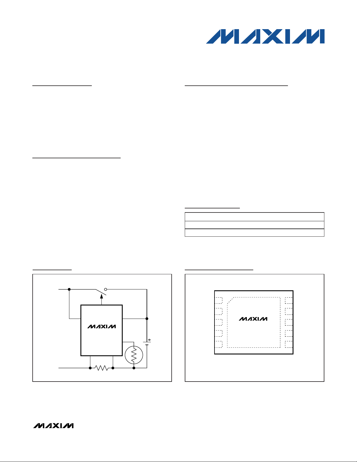
Typical Operating Circuit
Rev 0; 4/08
For pricing, delivery, and ordering information, please contact Maxim Direct at 1-888-629-4642,
or visit Maxim’s website at www.maxim-ic.com.
+
Denotes a lead-free/RoHS-compliant package.
T&R = Tape and reel.
*
EP = Exposed pad.
PART PIN-PACKAGE
DS2710G+ 10 TDFN-EP*
DS2710G+T& R 10 TDFN-EP*
TOP VIEW
+
110
SS
2 9 VN1CS
3 8 VN0V
DD
4 7 TMRTHM
*EP
5 6 CTESTSTATUS
*EXPOSED PAD.
DS2710
TDFN
(3mm × 4mm)
VP1V
Page 2
DS2710
Single-Cell NiMH Charger
2 _______________________________________________________________________________________2 _______________________________________________________________________________________
ABSOLUTE MAXIMUM RATINGS
RECOMMENDED DC OPERATING CONDITIONS
(4.0V ≤ VDD≤ 5.5V, TA= -20°C to +70°C.)
Stresses beyond those listed under “Absolute Maximum Ratings” may cause permanent damage to the device. These are stress ratings only, and functional
operation of the device at these or any other conditions beyond those indicated in the operational sections of the specifications is not implied. Exposure to
absolute maximum rating conditions for extended periods may affect device reliability.
Voltage Range on All Pins Relative to VSS............-0.3V to +6.0V
Continuous Source/Sink Current CS ...................................20mA
Continuous Source Current STATUS ..................................10mA
Operating Temperature Range ...........................-40°C to +85°C
Storage Temperature Range .............................-55°C to +125°C
Soldering Temperature...........................Refer to the IPC/JEDEC
J-STD-020 Specification.
DC ELECTRICAL CHARACTERISTICS
(4.0V ≤ VDD≤ 5.5V, TA= -20°C to +70°C, unless otherwise noted.)
PARAMETER SYMBOL CONDITIONS MIN TYP MAX UNITS
Supply Voltage VDD (Note 1) 4.0 5.5 V
Input Voltage Range CTEST, TMR, THM, VP1, VN1 -0.3 VDD V
Supply Current, VDD I
UVLO Threshold V
UVLO Hysteresis V
Output-Voltage Low, CS V
Output-Voltage High, CS V
Output-Voltage Low, STATUS V
Output-Voltage High, STATUS V
Threshold Voltage,
-V Termination
Current-Sense Reference
Voltage
Hysteres is, Current-Sense
Comparator
Propagation Time, Current-Sense
Comparator to Dri ver Output
CS Pin Pul lup Current ICS VDD < V
STATUS Pin Pulldown Current I
Depleted Cell Voltage Thresho ld V
Overcharge Voltage Threshold
Open Socket Voltage Threshold
Offset, V
PARAMETER SYMBOL CONDITIONS MIN TYP MAX UNITS
Operating mode (Note 2) 250 1000 μA
DD
VDD rising (Note 1) 3.5 3.9 V
UVLO
VDD falling from above V
UHYS
VDD = 5.0V, IOL = +20mA (Note 1) 1.0 V
OL1
VDD = 5.0V, IOL = -20mA (Note 1) 4.0 V
OH1
VDD = 5.0V, IOL = +2mA (Notes 1, 3) 0.50 V
OL2
VDD = 5.0V, IOH = -2mA (Notes 1, 3) 4.0 V
OH2
V
MAX-O PEN
- V
MAX-CHARGE
After t
-V
V
(Notes 1, 5)
IREF
V
HYS-
COMP
t
PDLY
STAT
LOW
V
MAX-
OPEN
V
MAX-
CHARGE
VOS (Note 7) 98 100 102 mV
Centered ~ 0.113V 18 23 27 mV
2mV overdrive/underdrive at trip thresho ld
(Notes 4, 6)
VDD < V
VP1 - VN1 0.9 1.0 1.1 V
VP1 - VN1, CS = high (Note 7) 1.55 1.65 1.75 V
VP1 - VN1, CS = low (Note 7) 1.64 1.75 1.86 V
(Note 4) 1.0 2.0 3.0 mV
THO
UVLO
UVLO
30 mV
UVLO
125 mV
-6 +6 %
0.1 μs
(Note 4) 2 10 μA
(Note 4) 2 10 μA
Page 3
DS2710
Single-Cell NiMH Charger
_______________________________________________________________________________________ 3
Note 1: Voltages relative to VSS.
Note 2: Specification does not include CS and STATUS pin currents.
Note 3: STATUS pin is active high.
Note 4: Specification is guaranteed by design.
Note 5: Specification applicable during charge cycle with T
A
= 0°C to +70°C.
Note 6: 50mV overdrive while connected to a pMOS transistor (such as ZXM62P02 from Zetex).
Note 7: V
BAT-MAX1
and V
BAT-MAX1
ranges never overlap.
Note 8: VT
HM-MIN
, V
THM-MAX
, and V
THM-STOP
are fixed ratios of VDD. Their ranges never overlap.
Note 9: Maximum allowable leakage on TMR to maintain SUSPEND state.
DC ELECTRICAL CHARACTERISTICS (continued)
(4.0V ≤ VDD≤ 5.5V, TA= -20°C to +70°C, unless otherwise noted.)
ELECTRICAL CHARACTERISTICS: TIMING
(4.0V ≤ VDD≤ 5.5V, TA= -20°C to +70°C, unless otherwise noted.)
Cold Temperature Detect
Threshold
Hot Temperature No-Start
Threshold
Hot Temperature Safety
Shutdown Threshold
SUSPEND Current Threshold I
Presence-Test Current, VP1 VDD 4.0V 1.0 10 15 μA
Reverse-Leakage Current, VP1 V
Impedance-Voltage Test Range V
PARAMETER SYMBOL CONDITIONS MIN TYP MAX UNITS
V
THM-MIN
V
THM-MAX
V
THM-ST OP
SUSP END
(Notes 1, 5, 8) 0.73 V
(Notes 1, 5, 8) 0.30 0.33 0.36 V
(Notes 1, 5, 8) 0.29 V
(Note 9) 0.1 0.5 μA
= 0V, VP1 = 1.5V 2 μA
DD
32 400 mV
CTEST
PARAMETER SYMBOL CONDITIONS MIN TYP MAX UNITS
Internal Time-Base Period t
Internal Time-Base Accuracy -10 +10 %
CS Output Duty Factor
CELL TEST Interval t
PRECHARGE Timeout t
FAST-CHARGE Termination
Hold-Off Period
FAST-CHARGE Flat Voltage
Timeout
Charge-Timer Period t
Charge-Timer Accuracy R
Charge-Timer Range t
CTMR -R ANGE
Toggle Rate, Charging f
Toggle Rate, FAULT State f
0.96 Seconds
BASE
DF1 FAST-CHARGE 96.9
DF2 PRECHARGE/TOP-OFF 25.0
DF3 MAINTENANCE 1.56
31 Seconds
CTST
V
PCHG
t
4 Minutes
THO
V
t
FLAT
R
CTMR
< V
CELL
not increasing 16 Minutes
CELL
= 40k 1.0 Hours
TMR
= 40k -6 +6 %
TMR
34 Minutes
LOW
0.5 5.0 Hours
1 Hz
CHARGE
4 Hz
FAULT
DD
DD
DD
%
Page 4
DS2710
Single-Cell NiMH Charger
4 _______________________________________________________________________________________
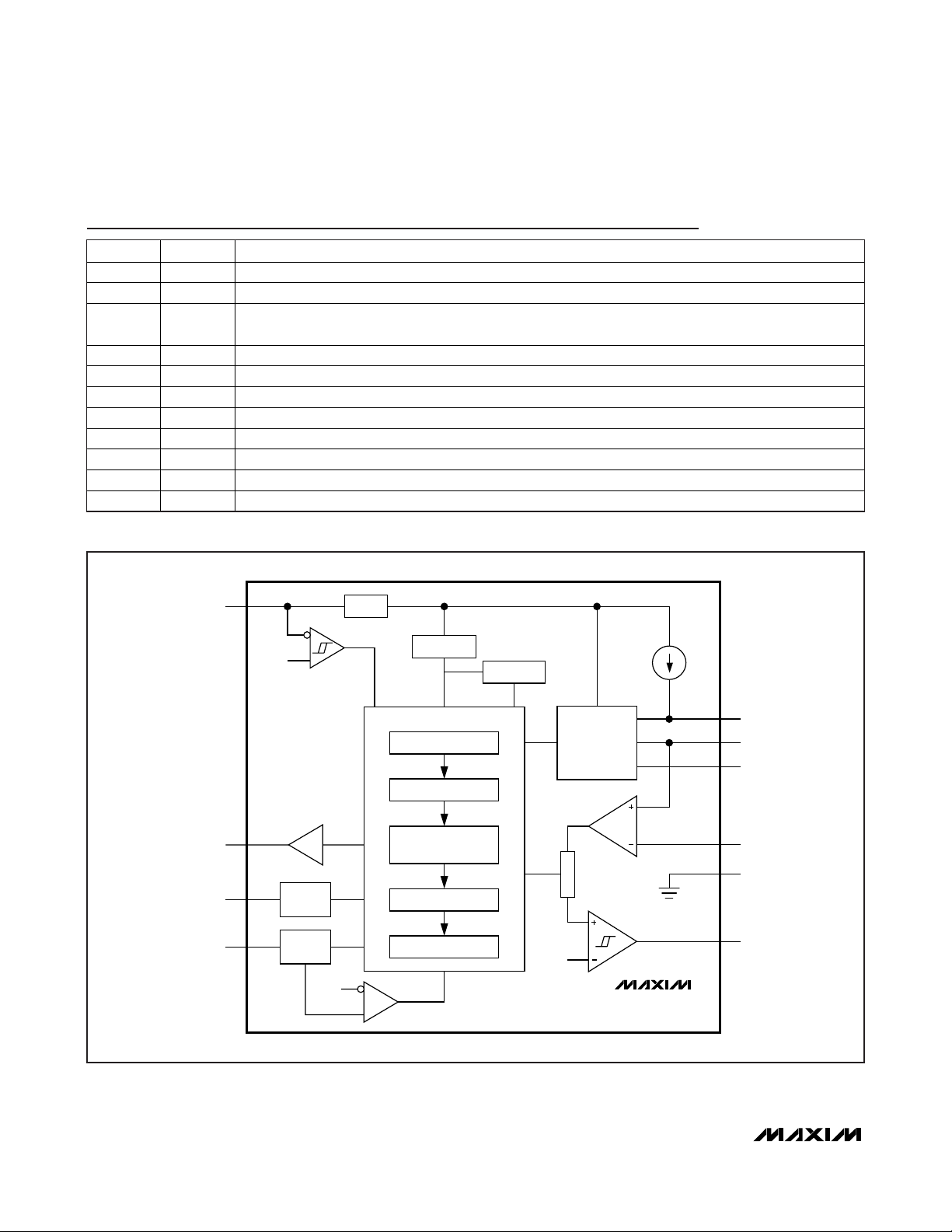
Pin Description
Figure 1. Block Diagram
PIN NAME FUNCTION
1 VSS Device Ground. Connect s directly to the negative terminal of the charge source.
2 CS Charge Source. Feedback control for switching circuitry.
3 V
4 THM Thermistor Input. Connects to a thermistor located near the cell and a resistor-div ider from the VDD pin.
5 STATUS Status Output. Drives an external LED or microprocessor input to indicate charge status.
6 CTEST Impedance Test. Connects to VSS through an external resistor to set the impedance-test threshold.
7 TMR Fast-Charge Timer. Connects to VSS through an external res istor to set the fast-charge timeout period.
8 VN0 Current-Sense Negative Input. Connects to the charge source s ide of the external sense resistor.
9 VN1 Current-Sense Positive Input. Connects to the cell side of the external sense resistor.
10 VP1 Cel l Voltage Sense. The voltage of the cel l is monitored through thi s input pin.
— EP Exposed Pad. Connects to VSS.
Power-Supply Input. Connects to the posit ive terminal of the charge source through a decoupling
DD
network.
V
STATUS
CTEST
TMR
0.1μA
BIAS
UVLO
OSCILLATOR
STATE MACHINE
PRESENSE TEST
PRECHARGE
FAST-CHARGE AND
CELL TESTS
TOP-OFF CHARGE
MAINTENANCE CHARGE
SUSPEND
WATCHDOG
ABORT
0.125V
VOLTAGE
AND
TEMPERATURE
MEASUREMENT
DUTYFACTOR
CONTROL
DS2710
I
PTST
VP1
VN1
THM
VN0
V
SS
CS
DD
3.5V
STATUS
CELL
TEST
CHARGE
TIMER
Page 5

Detailed Description
Charge Algorithm Overview
The DS2710 controls switch-mode topology charging of
a single NiMH cell from a voltage-regulated charge
source. The IC is reset in one of two ways: with the
application of power to the DS2710 or after exiting
SUSPEND state. Once one of these conditions occurs,
the DS2710 enters the PRESENCE state and waits for a
cell to be inserted before starting a charge cycle.
Once a cell is detected, the DS2710 enters PRECHARGE
state and begins qualification to prevent fast charging
of deeply depleted cells or charging under extreme
temperature conditions. Precharging is performed at a
reduced rate until the cell reaches 1V. The algorithm
then proceeds to the FAST-CHARGE state, which
includes cell tests to avoid accidental charging of alkaline cells or NiMH cells that are worn out or damaged.
Fast charging continues as long as all the cell qualification criteria are met. Fast charging terminates by the
-ΔV (negative delta voltage) method. The TOP-OFF
charge phase follows to completely charge the cell.
After the TOP-OFF charge timer expires, the DS2710
enters the MAINTENANCE state to indefinitely keep the
cell at a full state of charge. Maximum voltage, temperature, and charge-time monitoring during all charge
phases act as secondary or safety termination methods
to provide additional protection from overcharge. Any
error condition occurring during charge forces the
DS2710 into the FAULT state and charging terminates.
Charging can be halted at any time by floating the TMR
pin, which forces the DS2710 into SUSPEND state.
Once a charge is complete either normally or by
FAULT, the DS2710 remains in the final state (MAINTENANCE or FAULT) until the cell is removed, the IC is
power cycled, or the IC is forced into SUSPEND state.
Afterwards, the DS2710 returns to PRESENCE state
and the charge cycle begins again.
An internal oscillator provides the main clock source
used to generate timing signals for chip operation. The
PRECHARGE timer, hold-off timers, and timing for CS
operation and cell testing are derived from this time
base. If the internal clock should ever fail, a watchdogdetection circuit halts charging. The watchdog-safety
circuit and charge timer set by the TMR pin are derived
from oscillators other than the main clock source. Figure
1 is the DS2710 block diagram and Figure 2 is the state
diagram.
POWER-ON RESET (POR)
The UVLO circuit serves as a power-up and brownout
detector by monitoring VDDto prevent charging until
V
DD
rises above V
UVLO
, or when VDDdrops below
V
UVLO
- V
UHYS
. If undervoltage lockout is active,
charging is prevented, the state machine is forced to
the POR state, and all charge timers are reset.
PRESENCE
The DS2710 enters the PRESENCE state whenever the
TMR pin is not floating and VDD> V
UVLO
, indicating
that the charge source is present. The DS2710 remains
in the PRESENCE state until a cell is inserted into the
circuit, causing the voltage of VP1 - VN1 to fall below
1.65V (V
MAX-OPEN
) and the cell temperature is inside a
valid charging range between 0°C and +45°C
(T
THM-MIN
and T
THM-MAX
when used with recommended thermistor and resistor values). If both these conditions are met, the DS2710 enters PRECHARGE. If a cell
is inserted but the temperature is outside the valid
charging range, the DS2710 remains in the PRESENCE
state until the cell temperature falls within the valid
charging range.
PRECHARGE
The DS2710 enters the PRECHARGE state when a valid
cell voltage is detected and the cell temperature as
measured by the DS2710 thermistor circuit is within the
valid charging range. The DS2710 precharges the cell
by regulating the voltage drop across the sense resistor to 113mV with a 25% duty cycle. The STATUS output toggles at 1Hz to indicate the cell is being
precharged. Precharging lasts until the measured cell
voltage exceeds 1.0V (V
LOW
), at which time the
DS2710 enters the FAST-CHARGE state. If the cell voltage does not exceed V
LOW
within 30min (t
PCHG
) or if
the cell temperature exceeds +50°C (T
THM-STOP
) at
any time during PRECHARGE, the DS2710 enters the
FAULT state. If at any time during PRECHARGE the cell
voltage exceeds 1.75V (V
MAX-CHARGE
), the DS2710
determines that the cell has been removed and enters
the FAULT state.
FAST-CHARGE
In the FAST-CHARGE state, the DS2710 regulates the
average voltage across the sense resistor to 113mV.
The STATUS output is held high to indicate the cell
pack is being charged. During FAST-CHARGE, the
DS2710 performs a cell test every 31s. The CELL TEST
state is responsible for determining when charge is
complete. As secondary overcharge protection, the
DS2710 terminates FAST-CHARGE and enters TOPOFF based on a time delay set by the external resistor
on the TMR pin. This resistor value can set the secondary charge termination delay to anywhere from
30min up to 5hr. If the cell temperature exceeds +50°C
at any time during FAST-CHARGE, the DS2710 enters
DS2710
Single-Cell NiMH Charger
_______________________________________________________________________________________ 5
Page 6

DS2710
Single-Cell NiMH Charger
6 _______________________________________________________________________________________
Figure 2. State Diagram
> R
R
TMR
SUSPEND
CS = INACTIVE
> 1.0V
V
CELL
t < t
T < +50°C
POR
PRECHARGE
CS = ACTIVE 25% DF
STATUS = 1Hz TOGGLE
AND
PCHG
AND
PASS
31s INTERVAL
(ASYNCHRONOUSLY FROM ANYWHERE)
(ASYNCHRONOUSLY FROM ANYWHERE)
< V
V
- V
DD
UVLO
UHYS
t < t
PCHG
AND
< 1.0V
V
CELL
SUSPEND
CS = INACTIVE
STATUS = LOW
VDD > V
UVLO
V
CELL TEST
CS = INACTIVE
STATUS = HIGH
(3.5V)
V
CELL
t > t
T > +50°C
CELL
< V
MAX-OPEN
PCHG
OR
OR
> V
*
MAX
FAIL: V
OR ΔV > CTEST
R
< R
TMR
CELL
SUSPEND
PRESENCE
CS = INACTIVE
STATUS = LOW
STATUS = 4Hz TOGGLE
> V
MAX-OPEN
> 1.75V
V
CELL
FAULT
CS = INACTIVE
V
> V
CELL
MAX
*
> 1.75V
V
CELL
OR
T < 0°C
OR
T > +45°C
FAST-CHARGE
t < FAST TIMEOUT
CS = ACTIVE
STATUS = HIGH
t > FAST TIMEOUT
-ΔV DETECT
OR
T > +50°C
FLAT VOLTAGE DETECT
MAINTENANCE
CS = ACTIVE 1.56% DF
STATUS = LOW
t < TOP-OFF TIMEOUT
REPRESENTS V
*V
MAX
MAX-CHARGE
TOP-OFF
CS = ACTIVE 25% DF
STATUS = HIGH
WHEN THE CS OUTPUT IS ACTIVE AND V
T > +50°C
OR
t > TOP-OFF TIMEOUT
WHEN THE CS OUTPUT IS INACTIVE.
MAX-OPEN
V
> V
MAX
*
CELL
Page 7

the MAINTENANCE state. If at any time during FASTCHARGE the cell voltage exceeds V
MAX-CHARGE
, the
DS2710 determines that the cell is either overcharged
or has been removed, and enters the FAULT state.
CELL TEST
CELL TEST is performed once every 31s during FASTCHARGE to determine if charging is complete. During
CELL TEST, the CS output is held high to prevent
charging. The cell’s voltage is measured and compared against prior readings. The maximum cell voltage measurement during the charge is retained. If a
cell’s voltage falls more than 2mV (V
-ΔV
) from its peak
reading, the FAST-CHARGE terminates successfully
and moves to TOP-OFF. The DS2710 also moves to
TOP-OFF if the cell’s voltage reading does not exceed
the maximum over a 16min period (t
FLAT
). A hold-off
period for -ΔV and flat voltage detection begins at the
start of fast charging and prevents false termination in
the first 4min of the charge cycle (t
THO
).
The impedance of the cell is also measured during
CELL TEST. The cell’s open-circuit voltage is compared
against the voltage of the cell under charge. The difference is compared against the impedance threshold set
by the CTEST pin. If the difference exceeds the threshold set by CTEST, the cell’s impedance is considered
to be too high for charging and the DS2710 enters the
FAULT state. The DS2710 also enters FAULT state if
any voltage reading in CELL TEST exceeds the
V
MAX-OPEN
threshold.
TOP-OFF
In the TOP-OFF state, the DS2710 charges at 25% the
rate of FAST-CHARGE. The voltage across the sense
resistor is regulated to 113mV with a 25% duty cycle.
The STATUS output is held high to indicate the cell
pack is being charged. The charge timer is reset and
restarted with a timeout period of one-half the
FAST-CHARGE duration. When the charge timer
expires or if the measured temperature exceeds
+50°C, the charger enters the MAINTENANCE state. If
the cell voltage is greater than V
MAX-CHARGE
during
the 25% of time when charge current is applied or
V
MAX-OPEN
during the remaining time, TOP-OFF is exit-
ed early and the DS2710 goes to FAULT.
MAINTENANCE
The DS2710 enters the MAINTENANCE state whenever
the charge completes normally or if the measured cell
temperature exceeds +50°C during the charge. The
STATUS pin is driven low to indicate TOP-OFF has
completed. The cell’s state of charge is maintained
indefinitely by continuing a 1.56% duty-cycle charge of
the cell. The DS2710 remains in the MAINTENANCE
state until the cell is removed, the DS2710 is power
cycled, or the DS2710 is forced into SUSPEND state.
FAULT
The DS2710 can enter FAULT from any charge state if
the cell voltage exceeds V
MAX-CHARGE
any time when
charge current is applied (CS low) or V
MAX-OPEN
at any
time when no charge current is flowing (CS high). In
addition, FAULT can be entered during PRECHARGE if
the cell’s temperature exceeds +50°C or the
PRECHARGE timer expires, or during FAST-CHARGE if
impedance threshold is exceeded. In the FAULT state,
CS is forced high to prevent charging and the STATUS
output toggles at a 4Hz rate to indicate that an error
has occurred. The DS2710 remains in FAULT until a
cell voltage greater than 1.75V (V
MAX-CHARGE
) is
detected, indicating that the cell has been removed.
The DS2710 then enters the PRESENCE state and waits
for the next cell insertion.
SUSPEND
Suspension of charge activity is possible by floating the
TMR pin (R
TMR
> R
SUSPEND
). The CS output is pulled
to VDDto disable the charge control FET to prevent current flow to the cell. When the TMR connection is
restored, charging begins from the PRESENCE state
with all timers reset. The SUSPEND state is useful as a
means to stop charging by the application circuit, such
as with a microcontroller signal.
DS2710
Single-Cell NiMH Charger
_______________________________________________________________________________________ 7
Page 8

DS2710
Charge-Current Regulation
The DS2710 regulates charge current by maintaining a
constant average voltage across an external sense
resistor connected between the VN1 and VN0 pins.
VN1 and VN0 drive an internal comparator in the
DS2710 to switch the CS output ON and OFF to drive a
regulating pnp bipolar or a pMOS transistor. Hysteresis
on the comparator input provides noise rejection. The
DS2710 regulates the charge current during FASTCHARGE to maintain a voltage drop across the sense
resistor as follows:
V
SENSE
= V
IREF
- 0.5 x V
HYS-COMP
= 0.113V (typ)
Figure 3 shows the sense resistor voltage and CS pin
voltage of the regulating circuit during normal operation.
Charging with Load Applied
NiMH cells have a low, but finite, impedance. If load
current is flowing out of the battery, an internal voltage
drop appears at the battery terminals. This can interfere
with the CTEST and -ΔV detection. If the load current is
variable, early termination is more likely than if the load
current is constant. If the load’s ground is connected to
the negative terminal of the cell (VN0), load current
flows through the current-sense resistor, resulting in less
charge current to the battery. The load-current return
path should be to charger ground to reduce the likelihood of false termination or impedance-test errors.
Charging with load applied is not recommended.
Temperature Monitoring
Accurate temperature sensing is needed to detect temperature FAULT conditions. Connecting an external
10kΩ NTC thermistor between THM and VSSand a
10kΩ bias resistor between VDDand THM allows the
DS2710 to sense temperature. To accurately monitor
the cell, the thermistor should make physical contact
either to the cell or cell tabs. Table 1 shows several recommended 10kΩ thermistors.
MIN, MAX Temperature Compare
The voltage thresholds of the THM input (V
THM-MIN
,
V
THM-MAX
) are set to allow charging to start if the thermistor temperature is between 0°C and +45°C when
using the recommended 10kΩ bias resistor and 10kΩ
thermistor circuit. If precharging is in progress and the
voltage on THM reaches V
THM-STOP
, precharging
stops and a FAULT condition is generated. If the voltage on THM reaches V
THM-STOP
during FASTCHARGE or TOP-OFF, charging stops and the DS2710
enters the MAINTENANCE state. FAST-CHARGE and
Single-Cell NiMH Charger
8 _______________________________________________________________________________________
Figure 3. Ideal Comparator Input and Charge Control Output
Waveforms
Figure 4. Ratio of THM Pin to VDDPin Over Temperature
Table 1. THM Thresholds
THM THRESHOLD RATIO OF V
MIN 0.73 27.04 0 +4
MAX 0.33 4.925 +45 +42
STOP 0.29 4.085 +50 +47
NOT DRAWN TO SCALE
V
CS
V
SENSE
TIME
CBIAS
V
V
V
V
V
OH1
OL1
IREF
SENSE
IREF
(DC)
- V
HYS-COMP
THERMISTOR
RESISTANCE
(k)
TEMPERATURE (°C)
Fenwal
Semitec 103AT-2
0.75
0.70
0.65
0.60
0.55
0.50
0.45
VOLTAGE RATIO
0.40
0.35
0.30
0 1020304050
DIVIDER OUTPUT
TEMPERATURE (°C)
197-103LAG-A01,
173-103LAF-301
Page 9

TOP-OFF complete normally if the cell temperature
remains below this threshold.
Used with a 10kΩ resistor, the Semitec 103AT-2 provides approximately 0.9% full scale-per-degree sensitivity. Figure 4 shows this linearity curve. The left axis is
the ratio of the sensed voltage to the divider’s input
voltage (VDD).
Charge-Status Output
The DS2710 indicates the state of charge and the
charge results on the STATUS output pin. When no cell
is present, the output is driven to a logic-low. Any LED
attached to the STATUS pin is off. When a cell is inserted, STATUS oscillates in a 1Hz, 50% duty-cycle pattern
to indicate the cell is precharging. Once the DS2710
transitions to FAST-CHARGE, the STATUS output goes
to logic-high and stays high until the end of TOP-OFF.
STATUS returns to logic-low for MAINTENANCE charge
and remains at logic-low until the cell is removed or the
DS2710 is power cycled. If a FAULT occurs during
charging, STATUS toggles at a fast 4Hz, 50% dutycycle rate until the cell is removed. Table 2 summarizes
the STATUS output and LED operation for each charge
condition.
Charge-Rate Selection
The charge rate is determined by an external sense
resistor connected between the VN1 and VN0 pins. The
DS2710 regulates the charge current to maintain a voltage drop of V
IREF
- 0.5 x V
HYS-COMP
across the sense
resistor during FAST-CHARGE:
V
SENSE
= V
IREF
- 0.5 x V
HYS-COMP
= 0.113V (typ)
The sense resistor can therefore be selected by:
R
SENSE
= 0.113V/Desired FAST-CHARGE Current
The effective FAST-CHARGE rate is equal to 0.969 times
the regulated current limit, TOP-OFF rate is 0.25 times
the regulated current, and MAINTENANCE charge rate
is 0.0156 times the regulated current. Table 3 shows
the charge rates for charging three different cell capacities using a 565mA (0.200Ω sense) current source and
a 1130mA (0.100Ω sense) current source.
DS2710
Single-Cell NiMH Charger
_______________________________________________________________________________________ 9
Table 2. LED Display Patterns Based on Charge State
Table 3. Charge-Rate Examples
CHARGE STATE
NO BATTERY PRECHARGE
STATUS PIN Logic- low
STATUS PIN LED Off 1Hz toggle On Off 4Hz toggle
Oscillates at 1Hz,
50% duty cyc le
FAST-CHARGE/
TOP -OFF
Logic-high Logic-low
MAINTENANCE FAULT
Oscillates at 4Hz,
50% duty cyc le
565mA CHARGE RATE (0.200)
STATE
900mAH 1700mAH 2200mAH 900mAH 1700mAH 2200mAH
FAST-CHARGE C/1.64 C/3.10 C/4.00 C/0.82 C/1.55 C/2.0
PRECHARGE/TOP-OFF C/6.37 C/12.0 C/15.5 C/3.19 C/6.0 C/7.75
MAINTENANCE C/102 C/193 C/249 C/51 C/96 C/125
AT CELL CAPACITY
1130mA CHARGE RATE (0.100)
AT CELL CAPACITY
Page 10

DS2710
Timeout Selection
FAST-CHARGE state normally operates until -ΔV termination. In the event that termination does not occur correctly, a safety timeout is required. This timeout is set
by an external resistor on the TMR pin to VSSand provides secondary protection against significant overcharging. The value of the TMR resistor should be
chosen so that the timeout is greater than the FASTCHARGE time expected in the application, but not so
much greater that its protection is compromised. If the
timer expires during FAST-CHARGE, the timer count is
reset and charging proceeds to the TOP-OFF charge
state. The TMR resistor also sets the timed charge
duration of TOP-OFF state. The TOP-OFF timeout period is fixed at half the FAST-CHARGE timeout period.
When the timer expires in TOP-OFF, the DS2710 enters
the MAINTENANCE state.
Resistors can be selected to support FAST-CHARGE
timeout periods of 0.5hr to 5hr and TOP-OFF timeout
periods of 0.25hr to 2.5hr. The programmed FASTCHARGE time approximately follows the equation:
t(minutes) = 1.5 x R
TMR
(Ω)/1000
Impedance-Test Threshold
Selection
The DS2710 tests the cell impedance every 31s while
in FAST-CHARGE state. Impedance is measured by
comparing the cell voltage during normal charging to
the cell voltage with no charge current (CS output held
high). The resulting voltage difference is compared
against the threshold set by an external resistor from
CTEST to VSS. The detection threshold can be set from
32mV to 400mV. The following formula approximates
the setting for the detection threshold:
V
TEST
= 8000/R
CTEST
(Value in Volts)
Since the charge rate is controlled by the external
sense resistor (R
SENSE
) between VN1 and VN0, the test
threshold can be expressed as impedance as follows:
Impedance Threshold =
( 8000/R
CTEST
)/( 0.113/R
SENSE
) =
70796 x ( R
SENSE/RCTEST
)
For example, an application charging at 1.13A (R
SENSE
= 0.100Ω) would use a 47kΩ resistor on the CTEST pin
to set the impedance threshold to 0.150Ω.
Application Circuit
Figure 5 shows a typical DS2710 application circuit for
charging a NiMH cell from a USB port or other 5V
charge source capable of supplying 0.5A. Q1, L1, C2,
and D2 form a switching buck-regulator circuit controlled by the CS pin of the DS2710. Current is regulated through the current-sense resistor, R9, by switching
Q1 on and off as the sense resistor voltage ramps up
and down toward the preset sense voltage thresholds.
The 0.100Ω sense resistor along with the DC groundreferenced sense threshold level of V
IREF
- 1/2 V
HYS-
COMP
sets the average charge current in the example
to 1.13A. The sense resistor should have a proper
power rating for the chosen charge current.
The TMR resistor is set to 100kΩ for a timeout of 2.5hr.
This is appropriate for cells with a capacity of approximately 2200mAh when charged with the 1.13A charge
current. The CTEST resistor is set to 47kΩ for an impedance-test threshold of approximately 0.150Ω when
charging at 1.13A. Additionally, R6 protects the VP1 pin
from any stress applied to the exposed tabs of a loose
NiMH cell; R3 creates a weak pullup to offset the leakage through D2, which might otherwise cause a false
cell detection; and R1/C1 creates a bypass filter on the
V
DD
pin of the IC.
The value of L1 in Figure 5 represents a moderate
switching speed of ~ 200kHz for FAST-CHARGE state.
L1 can be adjusted to fit specific application goals as
long as the associated change in switching speed
does not exceed the circuit’s ability to maintain proper
regulation of the sense-resistor voltage. All capacitors
should be ceramic surface-mount types of good quality
where possible. The 10µF capacitor can be of any type
that meets the application requirements. All resistors
not previously mentioned are standard surface-mount
types.
Application PCB Layout
Proper layout rules must be followed to ensure a successful application circuit. For all modes of operation,
currents in excess of 1A can flow through the charge
and discharge paths (USB charging is specification limited to 500mA). All these paths should be properly sized
to handle the worst-case current flow, whether from
charging or from powering the load with the battery.
Switch-mode operation presents challenges with fast
voltage and current transients. Proper switch-mode
buck power-supply layout should always be observed.
Single-Cell NiMH Charger
10 ______________________________________________________________________________________
Page 11

DS2710
Single-Cell NiMH Charger
______________________________________________________________________________________ 11
Figure 5. Typical Application Circuit for USB Port Charging
Referring to the example circuit and layout of Figure 6,
the loop labeled as Loop1 encompassing CIN,
Q
SWITCH
, and D
SWITCH
should be kept as small as
possible to minimize the change in loop area that
occurs when switching from the OFF to the ON state
and vice versa. Loop2 should also be minimized as
much as practical, although it contains DC current
components for the most part. The returning ground
currents should be allowed to follow a path on a layer
directly under the outgoing path since the high-frequency components try to follow the path of least
impedance. Low ESR and ESL capacitors should be
used when possible and for all capacitors 10µF and
smaller. Typical surface-mount ceramic types with an
X5R or better dielectric are recommended.
Another important layout detail is the connection of the
sense resistor. Proper Kelvin connection layout should
be used to ensure the signal quality viewed by the
sensing circuit inside the DS2710 is adequate. Figure 7
shows a recommended connection of the sense lines to
the resistor footprint.
PACKAGE TYPE PACKAGE CODE DOCUMENT NO.
10 TDFN-EP —
56-G0012-001
Package Information
For the latest package outline information and land patterns, go
to www.maxim-ic.com/packages
.
R3
270kΩ
+5V
(USB+)
GROUND
(USB-)
1μF
Q1
ZXM62P02E6
R1
150Ω
R4
10kΩ
C1
RT1
103AT-2
10μF
CERAMIC
1kΩ
C2
CS
V
DD
THM
STATUS
R2
TMR CTEST V
D1
GREEN
SMA
R7
100kΩ
L1
15μH
SISCDRH74M-150R
D2
1W B340A-13
SCHOTTKY
DS2710
R8
47kΩ
C3
10μF
CERAMIC
R6
1kΩ
VP1
1S
NiMH
CELL
VN1
R9
0.1Ω
1W
VN0
SS
Page 12

DS2710
Single-Cell NiMH Charger
Maxim cannot assume responsibility for use of any circuitry other than circuitry entirely embodied in a Maxim product. No circuit patent licenses are
implied. Maxim reserves the right to change the circuitry and specifications without notice at any time.
12
____________________Maxim Integrated Products, 120 San Gabriel Drive, Sunnyvale, CA 94086 408-737-7600
© 2008 Maxim Integrated Products is a registered trademark of Maxim Integrated Products, Inc.
Figure 6. Switching Circuit with Example Layout
Figure 7. Sense Resistor Connection Layout
R
GATE
Q
SWITCH
CHARGE SOURCE SIDE
C
IN
LOOP1 LOOP2
CONTROL
D
SWITCH
LOOP AREAS MINIMIZED
L
SWITCH
C
OUT
BATTERY SIDE
CHARGE SOURCE SIDE
CONTROL
C
I
R
G
SENSE TRACES RUN CLOSE
SENSE+ SENSE-
R
SNS
CHARGE SOURCE- CHARGE SOURCE-
BATTERY- BATTERY-
TOGETHER TO MINIMIZE LOOP
Q
S
INDUCTANCE
D
S
L
S
SENSE+
C
O
SENSE-
R
SNS
BATTERY SIDE
BACKSIDE
GROUND PLANE
PROPER KELVIN CONNECTION
AT SENSE RESISTOR
 Loading...