

Page 1
r
m
PASS
FAIL
C
SHA-1 Authentication Maste
DS2705
www.maxim-ic.com
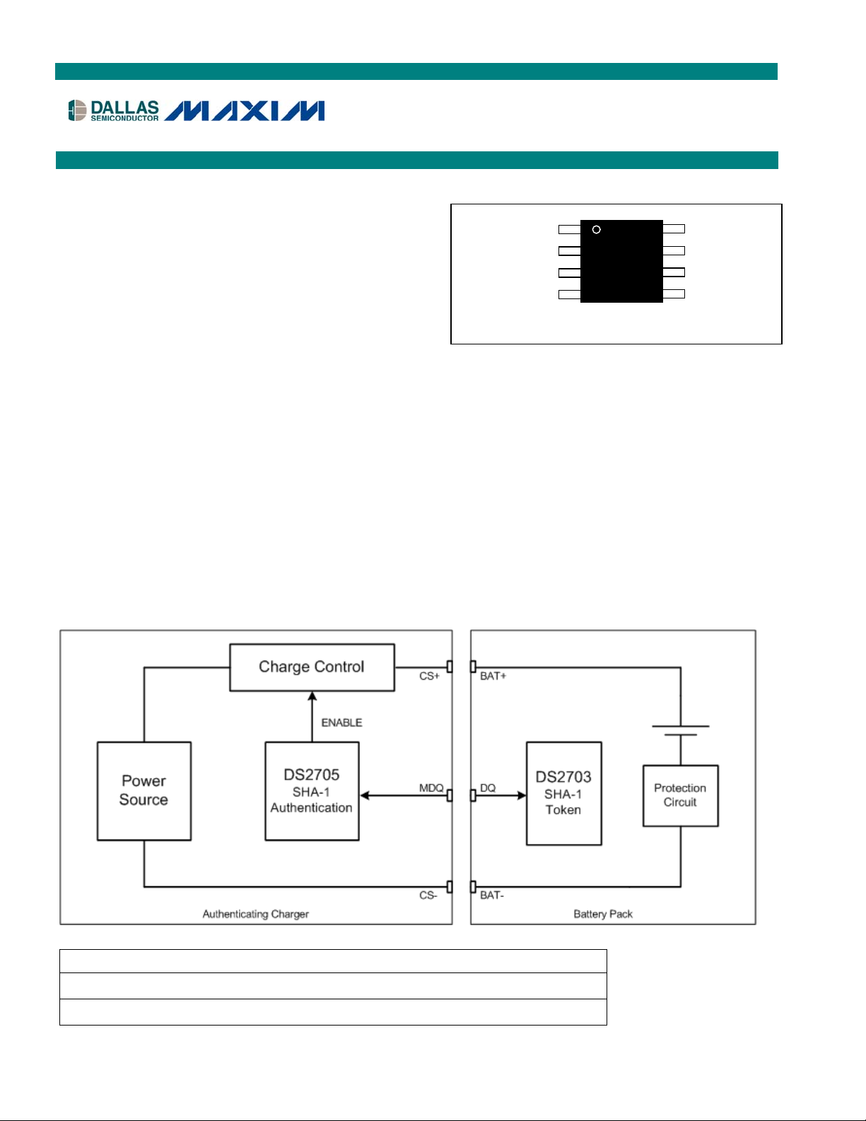
GENERAL DESCRIPTION
The DS2705 provides the master side of a Secure
Hash Algorithm (SHA) based token authentication
scheme. Hardware-based SHA authentication allows
for security without the added cost and complexity of
a microprocessor-based system. Batteries and other
accessories are authenticated using a single contact
through the Dallas 1-WireÒ interface. Authentication
is performed on demand or automatically, with the
pass/fail status reported on open-drain output pins to
signal the charge system and/or drive LEDs. The
DS2705 stores a predetermined challenge-andresponse pair in nonvolatile (NV) EEPROM. The
DS2705 works in conjunction with Dallas Battery
Management SHA-1 token products, including the
DS2703 and DS2704.
APPLICATIONS
Digital Cameras
Portable DVD and Media Players
Cradle and Accessory Chargers
Cell Phones/Smartphones
APPLICATION EXAMPLE
PIN CONFIGURATION
HAL
2
3
VSS
MAX
VDD
7
MDQ
6
SDQ
VPP
FEATURES
§ Initiates Challenge-and-Response
Authentication based on the SHA-1 Algorithm
§ Dallas 1-Wire Master/Slave Interface Operates
at Standard and Overdrive Speeds
§ Input and Output pins for Initiating Challenge
and Reporting Authentication Pass/Fail
§ Programmable Configuration
§ Operates from 2.5V to 5.5V Supply
§ Tiny mMAX Package (Pb-Free)
ORDERING INFORMATION
PART TEMP RANGE MARKING PIN-PACKAGE
DS2705U+
DS2705U+/T&R
+ Denotes lead-free package.
1-Wire is a registered trademark of Dallas Semiconductor.
1 of 18 050506
-40°C to +85°C
-40°C to +85°C
DS2705
DS2705 DS2705U+ in Tape-and-Reel
mMAX
Page 2

DS2705: SHA-1 Authentication Master
ABSOLUTE MAXIMUM RATINGS
Voltage Range on All Pins (except VPP), Relative to VSS -0.3V to +5.5V
Voltage Range on V
Pin, Relative to VSS -0.3V to +18V
PP
Continuous Source Current, MDQ 20mA
Operating Temperature Range -40°C to +85°C
Storage Temperature Range -55°C to +125°C
Soldering Temperature See IPC/JEDEC J-STD-020A Specification
Stresses beyond those listed under “Absolute Maximum Ratings” may cause permanent damage to the device. These are stress ratings only,
and functional operation of the device at these or any other conditions beyond those indicated in the operational sections of the specifications is
not implied. Exposure to the absolute maximum rating conditions for extended periods may affect device.
DC ELECTRICAL CHARACTERISTICS
(2.5V £ VDD £ 5.5V, TA = -20°C to +85°C.)
PARAMETER SYMBOL CONDITIONS MIN TYP MAX UNITS
Active mode,
MDQ low, I
Active mode,
MDQ idle, I
O_MDQ
O_MDQ
Sleep mode, I
= 0
= 0
= 0 (Note 2) 1 2
O_MDQ
2.5 mA
90 130
mA
mA
Program pulse (Notes 1, 3) 14.5 15.0 V
(Note 1) 1.8 V
(Note 1) 0.6 V
IOL = 4mA (Note 1) 0.4 V
Supply Current
Programming Voltage: VPP
Input Logic High:
MDQ, SDQ, CHAL
Input Logic Low:
MDQ, SDQ, CHAL
Output Logic Low: MDQ, SDQ V
I
I
I
V
V
V
DD1
DD2
DD3
PP
IH
IL
OL1
Output Logic Low: PASS, FAIL
Pulldown: VPP
Pulldown: SDQ, CHAL I
Pullup: MDQ
V
OL2
I
PD1
PD2
IOH
VOH
IOL = 10mA (Note 1) 0.4 V
300
(Note 5) 0.125
Communication mode
(Note 6)
Computation mode
= 2.0mA (Note 7)
I
OH
0.25 2.5 mA
V
- 0.1
DD
V
mA
mA
Input Capacitance: MDQ, SDQ CIN 60 pF
EEPROM RELIABILITY SPECIFICATION
(2.5V £ VDD £ 5.5V, TA = -20°C to +85°C.)
PARAMETER SYMBOL CONDITIONS MIN TYP MAX UNITS
EEPROM Write Time t
EEPROM Write Endurance N
EEW
EEC
(Note 3) 15 ms
(Notes 3, 4) 1,000 Cycles
2 of 18
Page 3

DS2705: SHA-1 Authentication Master
AC ELECTRICAL CHARACTERISTICS: MASTER 1-Wire INTERFACE
(2.5V £ VDD £ 5.5V, TA = -20°C to +85°C.)
PARAMETER SYMBOL CONDITIONS MIN TYP MAX UNITS
STANDARD BUS TIMING
Time Slot t
Recovery Time t
Write-0 Low Time t
Write-1 Low Time t
Read-Data Sample Window t
Reset-Time Low t
Presence-Detect High t
Presence-Detect Low t
OVERDRIVE BUS TIMING
Time Slot t
Recovery Time t
Write-0 Low Time t
Write-1 Low Time t
Read-Data Sample Window t
(Note 10) 90
MSLOT
(Note 10) 7.5 10 12.5
MREC
(Note 10) 88.5
MLOW0
(Note 10) 1.05 1.5 2.25
MLOW1
(Note 10) 4.0 5.5 7.0
MRDV
(Note 10) 510 680 850
MRSTL
(Note 10) 2 75
MPDH
(Note 10) 2 400
MPDL
(Note 10) 12
MSLOT
(Note 10) 1 2 2.5
MREC
(Note 10) 10.5
MLOW0
(Note 10) 0.35 0.5 0.65
MLOW1
(Note 10) 1.1 1.5 1.9
MRDV
ms
ms
ms
ms
ms
ms
ms
ms
ms
ms
ms
ms
ms
Reset-Time Low t
Presence-Detect High t
Presence-Detect Low t
(Note 10) 53 70 88
MRSTL
(Note 10) 2 7
MPDH
(Note 10) 2 41
MPDL
ms
ms
ms
3 of 18
Page 4

DS2705: SHA-1 Authentication Master
AC ELECTRICAL CHARACTERISTICS: SLAVE 1-Wire INTERFACE
(2.5V £ VDD £ 5.5V, TA = -20°C to +85°C.)
PARAMETER SYMBOL CONDITIONS MIN TYP MAX UNITS
STANDARD BUS TIMING
Time Slot t
Recovery Time t
Write-0 Low Time t
Write-1 Low Time t
Read-Data Valid t
Reset-Time High t
Reset-Time Low t
Presence-Detect High t
Presence-Detect Low t
OVERDRIVE BUS TIMING
Time Slot t
Recovery Time t
Write-0 Low Time t
Write-1 Low Time t
60 120
SLOT
1
REC
60 120
LOW0
1 15
LOW1
15
RDV
480
RSTH
480 960
RSTL
15 60
PDH
60 240
PDL
6 16
SLOT
1
REC
6 16
LOW0
1 2
LOW1
ms
ms
ms
ms
ms
ms
ms
ms
ms
ms
ms
ms
ms
Read-Data Valid t
Reset-Time High t
Reset-Time Low t
Presence-Detect High t
Presence-Detect Low t
2
RDV
48
RSTH
48 80
RSTL
2 6
PDH
8 24
PDL
ms
ms
ms
ms
ms
4 of 18
Page 5

AC ELECTRICAL CHARACTERISTICS
(2.5V £ VDD £ 5.5V, TA = -20°C to +85°C.)
PARAMETER SYMBOL CONDITIONS MIN TYP MAX UNITS
DS2705: SHA-1 Authentication Master
Programming Pulse Width t
Programming Pulse Rise Time t
Programming Pulse Fall Time t
Strong Pullup Delay Time t
Strong Pullup Period t
Challenge Delay Time t
Authentication Attempt Time t
FAIL Pin Pulse Frequency
17 ms
PPW
(Note 8) 0.5 5
PPR
(Note 8) 0.5 5
PPF
2 10
SPUD
24 34 48 ms
SPUP
45 65 85 ms
CHD
(Note 9) 61 490 ms
AAT
FOM = 1, 50% duty cycle 1.5 2 2.5 Hz
t
FPF
Note 1:
Note 2:
Note 3:
Note 4:
Note 5:
Note 6:
Note 7:
Note 8:
Note 9:
Note 10:
All voltages are referenced to V
IDD3 Sleep mode conditions:
CHAL pin inactive OR (CHAL active AND (PAA = 0 AND PPT = 00 AND FOM = 0 AND Initial Authentication sequence
complete))
[Above conditions disable the internal oscillator]
Programming temperature range is T
5 years data retention at 70°C
If CHAL pin left unconnected, CHP bit = 0 required for an authentication attempt to be initiated on power up. See Table 1.
Typical Communication mode MDQ pullup behavior equivalent to 3kW resistor.
Typical Computation mode MDQ pullup behavior approximates a 50W resistor.
Exceeding maximum rise and fall time specifications may affect device reliability.
t
= Retries per Attempt x (264bits x 90ms + 3 x (t
AAT
MAX[7 retries]: 490ms, MIN[no retries]: 61ms with standard timings
1. 1-Wire Master timings based on ±25% clock tolerance from nominal.
2. t
3. t
4. Bus rise time of ~1ms required to settle to logic high by t
[defined in design documentation] = t
RPDT
= t
MPDL-MAX
MRSTH-MIN
.
SS
– t
MPDH-MAX,
= 0°C to 50°C.
A
+ t
+ t
RSTH
MRSTH
) + t
MRSTL
MRSTL
represents the maximum presence pulse low time allowed from the slave.
) = [1 to 8] x (23.7ms + 3.54ms + 34ms)
SPUD
after MDQ released at t
MRDV
MLOW1
PIN DESCRIPTION
PIN
mMAX
TDFN
1 1 CHAL Challenge Strobe Input Pin. Initiates authentication. Active level/edge set by CHP bit.
2 2
3 3
4 4
5 5
6 6 SDQ
7 7 MDQ
8 8
SYMBOL FUNCTION
PASS
FAIL
V
SS
V
PP
Authentication “PASS” Result Open-Drain Output Pin
Authentication “FAIL” Result Open-Drain Output Pin (Programmable As Low Or Pulse)
Supply Return Pin, GND Reference for Logic Signals
EEPROM Programming Voltage Input
Slave Serial interface Data I/O Pin. Bidirectional data transmit and receive at 16kbps or
143kbps. Bus master must provide a weak pullup.
Master Serial interface Data I/O Pin. Bidirectional data transmit and receive at 16kbps or
143kbps. Provides a weak pullup in communication mode and strong pullup in
computation mode.
V
Supply Input Pin. Bypass to VSS with 0.1mF capacitor.
DD
ms
ms
ms
5 of 18
Page 6
Figure 1. Block Diagram
DS2705: SHA-1 Authentication Master
VDD
EEPROM
64-bit
Challenge
CHP = 0
160-bit MAC
16-bit
Configuration
Pullup
Control
CHAL
PASS
FAIL
Control FSM
t
+ t
CHD
AAT
VSS
1-Wire
Master /
Slave
MDQ
SDQ
DETAILED DESCRIPTION
The DS2705 orchestrates a challenge/response SHA-1 authentication procedure by accessing a Dallas Battery
Management SHA-1 Token product, such as the DS2703 or DS2704. The remote SHA-1 token is accessed with
the MDQ pin acting as the 1-Wire bus master. The DS2705 issues the appropriate 1-Wire command sequence on
MDQ to write the 64-bit challenge, initiates a SHA-1 computation in the token, and then reads back the 160-bit
MAC result. The DS2705 compares the 160-bit MAC received from the battery token with the preprogrammed
MAC. An exact bit for bit match is required for the authentication to be successful. The result of the operation,
PASS or FAIL, is indicated on active low status output pins which can be used to drive status LEDs and/or enable
cell charging.
The DS2705 can be configured to automatically authenticate by detection of a presence pulse on MDQ or
authentication can be controlled by the state of the CHAL input pin. The DS2705’s SDQ pin is a 1-Wire slave
interface for programming the behavior of the I.C.. All EEPROM values can be permanently locked to prevent
corruption.
Figure 2 shows a example application circuit for a standalone battery charger. The DS2705 is preprogrammed for
automatic authentication on MDQ and also contains a known good challenge/response pair. Programming occurs
during assembly through PCB test points shown on the right side of the circuit. When a battery pack is inserted into
the charger, a presence pulse on MDQ will cause the DS2705 to automatically authenticate the pack. The result of
the authentication will be displayed through the LEDs and the DS2705 will either enable or disable the charging
circuit.
6 of 18
Page 7

DS2705: SHA-1 Authentication Master
Figure 2. Typical Application Circuit
MDQ
Contac ts
from
Charger to
Battery
Pack
Contact
BAT+
Contact
BAT-
Contact
Control
Charge
Circuit
Charge
Circuit
VSS
Charge
Circuit
Enable
Charge Circuit
VDD
Charge Supply
330 330 1K 150
0.1µF
CHAL
FAIL
PASS
DS2705
MDQVDD
SDQ
VPP
VSS
150
5.6V 5.6V 18V
SDQ
150
150
Testpoint
VPP
Testpoint
VSS
Testpoint
DS2705
Assembly
Programmi ng
Interface
BATTERY TOKEN PRESENCE DETECTION
Authentication of a battery or peripheral first depends on the authentication host detecting the presence or insertion
(electrical connection) of the accessory to the host unit. The DS2705 supports insertion detection in four ways, two
use the CHAL pin and two use the MDQ pin:
t
1. CHAL pin at the active logic level on IC power-up (detected after challenge delay time
negative logic level is determined by the CHP bit.
2. CHAL pin edge trigger after power-up period. Positive or negative edge trigger is determined by the CHP
bit.
3. Detection of Asynchronous 1-Wire Presence Pulse by insertion of battery with 1-Wire device (token).
4. Periodic Authentication Attempt issuing a 1-Wire Reset on MDQ to test for presence of a 1-Wire token.
). Positive or
CHD
With cases 1 and 2 above, the CHAL pin acts as a detection trigger when pulled to a logic low or logic high. A split
contact on the battery ground or supply terminal can be used to connect the CHAL pin to the positive or negative
battery terminal when the battery is present. In case 1, when the battery is connected prior to powering up the host
system (which occurs often since the battery typically powers the host), presence is detected by sensing the logic
level on CHAL immediately after power-up of the DS2705. A configuration bit, CHP, allows the use of either polarity
of the CHAL pin. Table 1 shows the timing and sequence of events for detecting presence on power-up. In case 2
above, the DS2705 monitors the CHAL pin for a signal transition after the power-up period is complete. The
DS2705 detects an authentication attempt on a positive or a negative edge of CHAL depending on the state of the
CHP bit. Table 2 shows the timing and sequence of detecting presence with an edge on CHAL.
7 of 18
Page 8

DS2705: SHA-1 Authentication Master
Table 1. Presence Detection/Authentication on Power-up Using CHAL Pin
TIME FROM
POWER UP
CHAL PIN
t = N/A High 0 Not Present Armed Hi-Z
t < t
t
t > t
t > t
Low 0 Present Initiated Hi-Z
CHD
CHD
> t > t
CHD
CHD
+ t
Low 0 Present In Progress Hi-Z
AAT
Low 0 Present Complete Active
Pos Edge 0 Removal Reset Reset (Hi-Z)
+ t
+ t
CHD
AAT
AAT
t = N/A Low 1 Not Present Armed Hi-Z
t < t
t
t > t
t > t
t
RTA1:0 bits. Minimum time is t
Table 2. Insertion Detection/Authentication Using Transition On CHAL Pin
High 1 Present Initiated Hi-Z
CHD
> t > t
CHD
CHD
CHD
: Authentication attempt time represents the period for attempting authentication and is dependent on the
AAT
+ t
High 1 Present In Progress Hi-Z
AAT
High 1 Present Complete Active
Neg Edge 1 Removal Reset Reset (Hi-Z)
SHA
+ t
+ t
CHD
AAT
AAT
CHAL PIN CHP BIT TOKEN PRESENCE AUTHENTICATION DISPLAY
High 0 Not Present Armed Hi-Z
Neg Edge 0 Insertion Initiated Hi-Z
Low < t
Low > t
CHD
CHD
+ t
0 Present In Progress Hi-Z
AAT
+ t
0 Present Complete Active
AAT
Pos Edge 0 Removal Reset Reset
Low 1 Not Present Armed Hi-Z
Pos Edge 1 Insertion Initiated Hi-Z
High < 0.5s 1 Present In Progress Hi-Z
High > 0.5s 1 Present Complete Active
Neg Edge 1 Removal Reset Reset
CHP
BIT
TOKEN
PRESENCE
, maximum time is 8*t
SHA
AUTHENTICATION DISPLAY
.
Detection cases 3 and 4 occur through a 1-Wire Reset/Presence Detect sequence on the MDQ pin. In case 3, an
asynchronous 1-Wire presence pulse occurs when a battery with a 1-Wire device is connected to the DS2705. The
DS2705 responds with the authentication sequence. Case 4 is a user configuration option where a 1-Wire reset is
periodically issued on MDQ which then monitors the bus for the presence pulse issued by any/all 1-Wire slave
devices on the bus. If the DS2705 detects a presence pulse, it begins an authentication sequence. The DS2705
can also be configured to periodically test for the continued presence of a 1-Wire slave device once successful
authentication has completed. This allows the status display to be automatically reset when a slave token has been
removed. Table 3 shows the sequence and display activity for presence detection on MDQ.
Table 3. Asynchronous And Periodic Presence Detection Using MDQ Pin
PD
No PD Not Present Reset Hi-Z
PD
No PD Removal Reset Reset (Hi-Z)
TOKEN
PRESENCE
AUTHENTICATION DISPLAY
Insertion Initiated Hi-Z
Present
In Progress Hi-Z
Complete Active
8 of 18
Page 9

DS2705: SHA-1 Authentication Master
AUTHENTICATION SEQUENCE
Following the detection of the battery, the DS2705 initiates the authentication sequence. The sequence is executed
in whole each time authentication is initiated. See Figure 4.
1. Test for presence with 1-Wire RESET.
2. Issue SKIP ROM (SKIP NET ADDRESS) command.
3. Issue Write Challenge command with 64-bit Challenge data.
4. Issue Compute MAC without ROMID command to SHA-1 token.
5. Provide strong pullup on DQ output.
6. Issue 8 write 0 timeslots.
7. Issue read time slots to receive MAC from token.
8. Compare local and token MAC results.
9. If configured for multiple attempts, re-try until authentication complete.
10. Test for presence with 1-Wire RESET.
11. Update status on
Note: If the DS2705 does not receive a presence pulse after presence has been established, or the presence
test in step 9. fails, then the status is reported as not present with both the
PASS or FAIL pins.
PASS and FAIL pins hi-Z.
PREPROGRAMMED CHALLENGE AND RESPONSE
A challenge response authentication system does not require a truly random set of challenges. The set of unique
challenges must be sufficiently large that it precludes the use of a lookup table type of attack. If a large enough set
of unique challenges is dispersed over a population of portable devices, then each portable device does not need
to store the secret key and duplicate the computation of the MAC. It need only store one challenge response pair to
provide a practical barrier to battery clones. This system requires that every battery contain the secret key and
SHA-1 algorithm so that it is compatible with any portable device it might be required to power.
The DS2705 stores the preprogrammed challenge and response MAC. This serves to lower the cost and increase
the secrecy of the key since the key does not have to be programmed into the DS2705. Dallas Semiconductor
recommends not using any challenge response pair where either the challenge or MAC is all ‘0’s or all ‘1’s to
prevent accidental authentication of an open or shorted communication bus.
9 of 18
Page 10

DS2705: SHA-1 Authentication Master
MASTER PORT (MDQ) FUNCTION COMMANDS
MASTER MODE WRITE CHALLENGE COMMAND
Write Challenge [0Ch, XXXXXXXXXXXXXXXX]. The master mode Write Challenge command sends the 8-byte
(64-bit) challenge to the remote token in preparation for a Compute MAC command.
Figure 3. Write Challenge (MDQ)
1-Wire
Reset
SKIP ROM
Cmd
Write
Challenge
64 Write Time Slots
(Random Number)
CMD
Presence
Pulse
MASTER MODE COMPUTE MAC W/O ROM ID COMMAND
Compute MAC without ROM ID [36h, XXXXXXXXXXXXXXXXXXXXXXXXXXXXXXXXXXXXXXXX].
The Compute MAC command executes a MAC computation in the remote token and reads back the 20-byte result.
Figure 4. Compute and Return MAC (MDQ)
t
SPUP
Strong
Pull-up Applied
8 Write 0
Time Slots
160 Read Time Slots
(20-By te MAC)
1-Wire
Reset
Presence
Pulse
SKIP ROM
Cmd
Compute
MAC
Cmd
t
SPUD
10 of 18
Page 11

DS2705: SHA-1 Authentication Master
MAC Comparison
After the SHA-1 computation is completed by the remote token, the DS2705 and remote SHA-1 token both contain
a MAC result based on the secret key. The results are compared by the DS2705 on a bit by bit basis as the MAC
data is read in from the remote token. Note that the secret is never transmitted on the bus and thus cannot be
captured by observing bus traffic.
Multiple Authentication Attempts
The DS2705 is configurable for multiple authentication attempts or re-tries to avoid reporting authentication failure
in the event of contact bounce or a noisy communication channel. When configured for more than one retry, the
status outputs are kept at the previous state until one attempt succeeds or all attempts fail. It is always
recommended to configure the DS2705 for at least one retry.
Signaling Authentication Results
Authentication results are signaled on the open drain
both outputs remain at their previous state. After authentication is complete, the pass or fail status is reported until
the display is cleared by one of the following conditions:
§ CHAL pin returning to inactive logic level.
§ Battery token removal detected when no 1-Wire Presence Pulse is returned in response to a 1-Wire
Reset.
PASS and FAIL output pins. During an authentication attempt,
Table 4. PASS/FAIL Outputs
CONDITION FOM BIT
Token Not Present x Hi-Z Hi-Z
Authentication in
Progress
Complete: Pass x LOW Hi-Z
Complete: Fail
x No Change No Change
0 Hi-Z LOW
1 Hi-Z Pulse
PASS OUTPUT FAIL OUTPUT
PROGRAMMING AND CONFIGURING
The DS2705 requires a configuration step prior to deployment to program the 64-bit challenge, 160-bit response
and to set up desired configuration options. Configuration is performed in slave mode using the SDQ and VPP
pins. The Challenge-and-Response pair, and option data are programmed in on-chip EEPROM that requires an
externally supplied programming voltage. After programming and verifying the EEPROM data, setting of the Lock
bits is recommended to prevent future modification. SDQ and VPP have internal pull downs which prevent the pins
from floating during normal operation.
11 of 18
Page 12

DS2705: SHA-1 Authentication Master
Table 5. Configuration Register
FIELD NAME DESCRIPTION DEFAULT
Re-Tries Per Authentication Attempt
Each re-try includes:
OWR, PD, Skip ROM, Write Challenge, Read MAC, Compare MAC, Final OWR/PD
0 0 0 Re-try (1 attempt per initiation)
CR[1:0] RTA1:0
CR[3:2] PAA1:0
CR[5:4] PPT1:0
CR[6] APA
CR[7] CHP
CR[8] FOM
CR[9] OWS
CR[11:10] LOCK1:0
0 1 1 Re-tries (2 attempts per initiation)
1 0 3 Re-tries (4 attempts per initiation)
1 1 7 Re-tries (8 attempts per initiation)
PASS output hi-Z until authentication complete.
Authentication complete after first occurrence of a PASS result or all re-tries are a FAIL result
Periodic Authentication Attempt
Each Attempt performed with the programmed number of re-tries:
0 0 No Periodic Attempts
0 1 Attempt every 1s
1 0 Attempt every 8s
1 1 Attempt every 16s
PASS and FAIL pins retain previous states until updated when authentication completed. If
presence not detected, status outputs are cleared to hi-Z.
Periodic Presence Test
1-Wire Presence test performed at programmed period:
0 0 No Periodic Test
0 1 Attempt every 0.25s
1 0 Attempt every 0.5s
1 1 Attempt every 1.0s
PASS and FAIL pins retain previous states if presence detected. PASS and FAIL pins are cleared to
hi-Z and status flags are cleared to zero if presence not detected.
Asynchronous Presence Authentication
0 No
1 Yes
Authentication sequence initiated t
CHAL Pin Polarity Setting
0 High to low transition; active low
1 Low to high transition; active high
FAIL Output Select
0 FAIL pin held low
1 FAIL pin pulsed low at 2Hz 50% duty cycle
1-Wire Bus Speed
0 Standard 1-wire communication (Master and Slave)
1 Overdrive 1-wire communication (Master and Slave)
EEPROM Lock
0 0 No Operation
0 1 No Operation
1 0 Permanently Lock EEPROM
1 1 No Operation
Writing a 10b to the lock bits, followed by an EEPROM copy will permanently lock all EEPROM
locations inside the DS2705. Writing any other value to the lock bits will perform no operation.
ms delay after Presence Detect from token.
CHD
00b
00b
00b
0b
0b
0b
0b
00b
CR[12]
¾
CR[13] FAILF
CR[14] PASSF
CR[15] LOCKF
RESERVED
FAIL flag. Mirrors the FAIL pin output for test via slave interface (SDQ pin). Set if authentication
attempt fails. Cleared when subsequent authentication attempt initiated.
PASS flag. Mirrors the PASS pin output for test via slave interface (SDQ pin). Set if authentication
attempt passes. Cleared when subsequent authentication attempt initiated.
Displays Lock/Unlock Status. LOCKF = 1 if lock procedure successful.
12 of 18
0b
0b
0b
0b
Page 13

DS2705: SHA-1 Authentication Master
MEMORY
The DS2705 has a 256 byte linear memory space for the EEPROM memory block that stores the challenge,
response and configuration parameters. Addresses designated as “Reserved” typically return FFh when read.
These bytes should not be written. EEPROM memory consists of non-volatile EEPROM cells overlaying volatile
shadow RAM. The Read Data and Write Data protocols allow the 1-Wire interface to directly accesses the shadow
RAM. The Copy Data and Recall Data function commands transfer data between the EEPROM cells and the
shadow RAM. In order to modify the data stored in the EEPROM cells, data must be written to the shadow RAM
and then copied to the EERPOM. In order to verify the data stored in the EEPROM cells, the EEPROM data must
be recalled to the shadow RAM and then read from the shadow. After issuing the Copy Data function command, a
programming pulse is required on the VPP pin.
Figure 5. EEPROM Access via Shadow RAM
Copy
EEPROM
Shadow RAM
Recall
Serial
Interface
Write
Read
Table 6. Memory Map
ADDRESS (HEX) DESCRIPTION READ/WRITE
00 to 07 64-bit Challenge R/W
08 to 1B 160-bit Response (Local MAC) R/W
1C to 1D Configuration Register R/W
1E to FF Reserved —
1-Wire BUS SYSTEM
The 1-Wire bus is a system that has a single bus master and one or more slaves. A multidrop bus is a 1-Wire bus
with multiple slaves, while a single-drop bus has only one slave device. The DS2705 acts as a bus master on the
MDQ pin and as a slave device on the SDQ pin. In both cases, the DS2705 requires a single-drop bus
configuration. The discussion of the 1-Wire bus system consists of three topics: hardware configuration, transaction
sequence, and 1-Wire signaling.
HARDWARE CONFIGURATION
Because the 1-Wire bus has only a single line, it is important that each device on the bus be able to drive it at the
appropriate time. To facilitate this, each device attached to the 1-Wire bus must connect to the bus with open-drain
or tri-state output drivers. The DS2705 uses an open-drain output driver as part of the bidirectional interface
circuitry shown in Figure 6. If a bidirectional pin is not available to act as the bus master when communicating with
the DS2705 as a slave on the SDQ pin, separate output and input pins can be connected together.
The 1-Wire bus must have a pullup resistor at the bus-master end of the bus. The DS2705 internally provides the
pullup for communication as a master on the MDQ pin. The bus master communicating with the DS2705 on SDQ is
responsible for providing an external pullup . The idle state for the 1-Wire bus is high. If, for any reason, a bus
transaction must be suspended, the bus must be left in the idle state to properly resume the transaction later. Note
that if the bus is left low for more than t
pulse, which effectively terminates the transaction.
, slave devices on the bus begin to interpret the low period as a reset
LOW0
13 of 18
Page 14

Figure 6. 1-Wire Bus Interface Circuitry, DS2705 as Slave
Vpullup
(2.5 to 5.5V)
1.5kW - 4.7kW
Test System Bus
Master
(approx.)
SDQ
DS2705 SDQ Port
DS2705: SHA-1 Authentication Master
Rx
~100 Ohm
MOSFET
Tx
~1 uA
Rx = Receive
Tx = Transmit
Rx
Tx
TRANSACTION SEQUENCE
The protocol for 1-Wire communication is as follows:
§ Initialization
§ Net Address Command
§ Function Command(s)
§ Data Transfer (not all commands have data transfer)
All transactions of the 1-Wire bus begin with an initialization sequence consisting of a reset pulse transmitted by the
bus master, followed by a presence pulse transmitted by a slave if it is present on the bus. The presence pulse tells
the bus master that a slave device is on the bus and ready to operate. For more details, see the 1-Wire Signaling
section.
NET ADDRESS COMMANDS
Once the bus master has detected the presence of a slave, it can issue the net address command described in the
following paragraph. The name of the Net Address command (ROM command) is followed by its 8-bit opcode in
square brackets.
Skip Net Address [CCh]. The only net address command supported by the DS2705 is the Skip Net Address
command. It is preserved on the DS2705 for compatibility with multidrop enabled slaves such as the DS2703/4.
Skip Net Address must also be used after a reset pulse when a bus master is communicating to the DS2705 over
the SDQ input.
SLAVE PORT (SDQ) FUNCTION COMMANDS
After successfully completing the Skip Net Address command, the bus master can access the features of the
DS2705 with any of the function commands described in the following paragraphs. The name of each function is
followed by the 8-bit opcode for that command in square brackets. The function commands are summarized in
Table 7.
Read Data [69h, XX]. This command reads data starting at memory address XX. The LSb of the data in address
XX is available to be read immediately after the MSb of the address has been entered. Because the address is
automatically incremented after the MSb of each byte is received, the LSb of the data at address XX + 1 is
available to be read immediately after the MSb of the data at address XX. If the bus master continues to read
beyond address FFh, data is read starting at memory address 00 and the address is automatically incremented
until a reset pulse occurs. Addresses labeled “Reserved” in the memory map contain undefined data values. The
read data command can be terminated by the bus master with a reset pulse at any bit boundary. Read Data from
returns the data in the shadow RAM. A Recall Data command is required to transfer data from the EEPROM to the
shadow. See the Memory section for more details.
14 of 18
Page 15

DS2705: SHA-1 Authentication Master
Write Data [6Ch, XX]. This command writes data starting at memory address XX. The LSb of the data to be stored
at address XX can be written immediately after the MSb of address has been entered. Because the address is
automatically incremented after the MSb of each byte is written, the LSb to be stored at address XX + 1 can be
written immediately after the MSb to be stored at address XX. If the bus master continues to write beyond address
FFh, the data starting at address 00 is overwritten. Writes to read-only addresses, reserved addresses and locked
EEPROM blocks are ignored. Incomplete bytes are not written. Write Data modifies the shadow RAM. A Copy Data
command is required to transfer data from the shadow to the EEPROM. See the Memory section for more details.
The Write command will cause spurious behavior if issued during an authentication attempt is in progress on the
MDQ pin.
Copy Data [48h]. This command copies the contents of all shadow RAM locations to EEPROM cells. After the
copy command is issued a high voltage pulse must be applied to the VPP pin for a time period of
t
. See Figure 7
PPW
for example bus timing of an EEPROM program function. During the pulse, the bus master can issue read timeslots
on the bus. The DS2705 will respond with ‘0’s while the EEPROM copy is in progress, and ‘1’s after the copy is
complete. A reset on SDQ at any time during the copy sequence will prematurely terminate the operation.
Figure 7. Copy EEPROM Sequence
t
t
PPR
PPW
t
PPF
VPP = 14.5V MIN
15.0V MAX
VPP
VPP = 0V
Non-critical Timing
SDQ
1-W ire
Reset
SKIP ROM
Cmd
Copy Data
Cmd
Presence
Pulse
Recall Data [B8h]. This command recalls the contents of all EEPROM cell locations to the shadow RAM memory.
Following the Recall command, SDQ must be driven low for a minimum of t
after the Recall command. The Recall command will cause spurious behavior if issued while an authentication
attempt is in progress on the MDQ pin.
Bus master may issue read slots during
EEPROM copy. DS2705 responds with
‘0’s during copy , ‘1’s afterwards.
. SDQ can be driven low indefinitely
RSTL
15 of 18
Page 16

Table 7. Slave Function Commands
COMMAND DESCRIPTION
COMMAND
PROTOCOL
DS2705: SHA-1 Authentication Master
BUS STATE
AFTER
COMMAND
PROTOCOL
BUS DATA
RESET
CCh
69h
Address
RESET
CCh
6Ch
Address
RESET
CCh
48h
Program Pulse
RESET
CCh
B8h
Master Rx
Master Tx
Master Rx
Master Reset None
Up to 256 bytes of
data
Up to 256 bytes of
data
Read data = 0 until
command completes
Read Data
Write Data
Copy Data
Recall Data
Reads data from
memory starting at
address XX
Writes data to
memory starting at
address XX
Copies shadow RAM
data to EEPROM
Recalls EEPROM to
shadow RAM
16 of 18
Page 17

DS2705: SHA-1 Authentication Master
I/O SIGNALING
The 1-Wire bus requires strict signaling protocols to ensure data integrity. The four protocols used in 1-Wire
communication are as follows: the initialization sequence (reset pulse followed by presence pulse), write 0, write 1,
and read data. The 1-Wire bus master initiates all these types of signaling except the presence pulse.
The initialization sequence required to begin any 1-Wire communication is shown in Figure 8. A presence pulse
following a reset pulse indicates that the 1-Wire slave is ready to accept a net address command. The bus master
transmits (Tx) a reset pulse for t
1-Wire bus line is then pulled high by the pullup resistor. After detecting the rising edge on the DQ pin, the slave
waits for t
and then transmits the presence pulse for t
PDH
Figure 8. 1-Wire Initialization Sequence
RESET PRESENCE PULSE
t
V
PULLUP
GND
. The bus master then releases the line and goes into receive mode (Rx). The
RSTL
.
PDL
MRSTL
t
MPDH
t
MPDL
MODE
Standard
Overdrive
680ms
70ms
4
4ms
0
s
m
640ms
160ms
64ms
16ms
LINE T YPE LEGEND:
Bus Master active LOW Device active LOW
Both Bus Master and Device Resistor pullup
active LOW
WRITE-TIME SLOTS
A write-time slot is initiated when the bus master pulls the 1-Wire bus from a logic-high (inactive) level to a logic-low
level. There are two types of write-time slots: write 1 and write 0. All write-time slots must be t
a 1ms minimum recovery time, t
t
LOW0_MIN
after the line falls. If the line is high when sampled, a write 1 occurs. If the line is low when sampled, a
write 0 occurs. The sample window is illustrated in Figure 9. 1-Wire Write and Read-Time
, between cycles. The slave samples the 1-Wire bus line between t
REC
Slots. For the bus master
in duration with
SLOT
LOW1_MAX
and
to generate a write 1 time slot, the bus line must be pulled low and then released, allowing the line to be pulled high
less than t
after the start of the write time slot. For the host to generate a write 0 time slot, the bus line must be
RDV
pulled low and held low for the duration of the write-time slot.
READ-TIME SLOTS
A read-time slot is initiated when the bus master pulls the 1-Wire bus line from a logic-high level to a logic-low level.
The bus master must keep the bus line low for at least 1ms and then release it to allow the slave to present valid
data. The bus master can then sample the data t
time slot, the slave releases the bus line and allows it to be pulled high by the external pullup resistor. All read-time
slots must be t
in duration with a 1ms minimum recovery time, t
SLOT
specifications in the Electrical Characteristics table for more information.
from the start of the read-time slot. By the end of the read-
RDV
, between cycles. See Figure 9 and the timing
REC
17 of 18
Page 18

Figure 9. 1-Wire Write and Read-Time Slots
WRITE 0 SLOT WRI TE 1 SLOT
DS2705: SHA-1 Authentication Master
V
PULLU P
GND
MODE
Standard
Overdrive
V
PULLU P
15ms
2ms
t
RDV
t
SLOT
t
LOW0
Slave Sample Window
MIN TYP MAX
15ms 30ms
1ms 3ms
Data = 0
t
SLOT
t
REC
15ms
2ms
READ DATA SLOT
t
REC
t
RDV
t
SLOT
t
LOW1
Slave Sample Window
MIN TYP MAX
15ms 30ms
1ms 3ms
Data = 1
t
SLOT
GND
t
LOW1
Master Sample Window
15ms
MODE
Standard
Overdrive
Master Sampl e Window
15ms
2ms 2ms
LINE TYPE LEGEND:
Bus Master active LOW Slave active LOW
Both Bus Master and Device Resistor pullup
active LOW
PACKAGE INFORMATION
(For the latest package outline information, go to www.maxim-ic.com/DallasPackInfo.)
18 of 18
 Loading...