

Page 1
www.maxim-ic.com
GENERAL DESCRIPTION
The DS25LV02 provides data storage and serial
number identification for battery packs. The lowvoltage Dallas 1-WireÒ interface enables serial
communication on a single battery contact and the
64-bit unique serial number allows multidrop
networking and identification of individual devices.
The 1024-bit EPROM memory is organized as 4
pages of 32 bytes each and supports storage of
battery cell characteristics, charging voltage, current
and temperature parameters, as well as battery pack
manufacturing data. CRC verification provides data
integrity during communication. The EPROM pages
are in-circuit writable and can be individually locked
to protect data. The DS25LV02 is designed to be
completely backward-compatible with the DS2502 for
existing designs.
APPLICATIONS
Cell Phones/Smartphones
Digital Cameras
MP3 Players
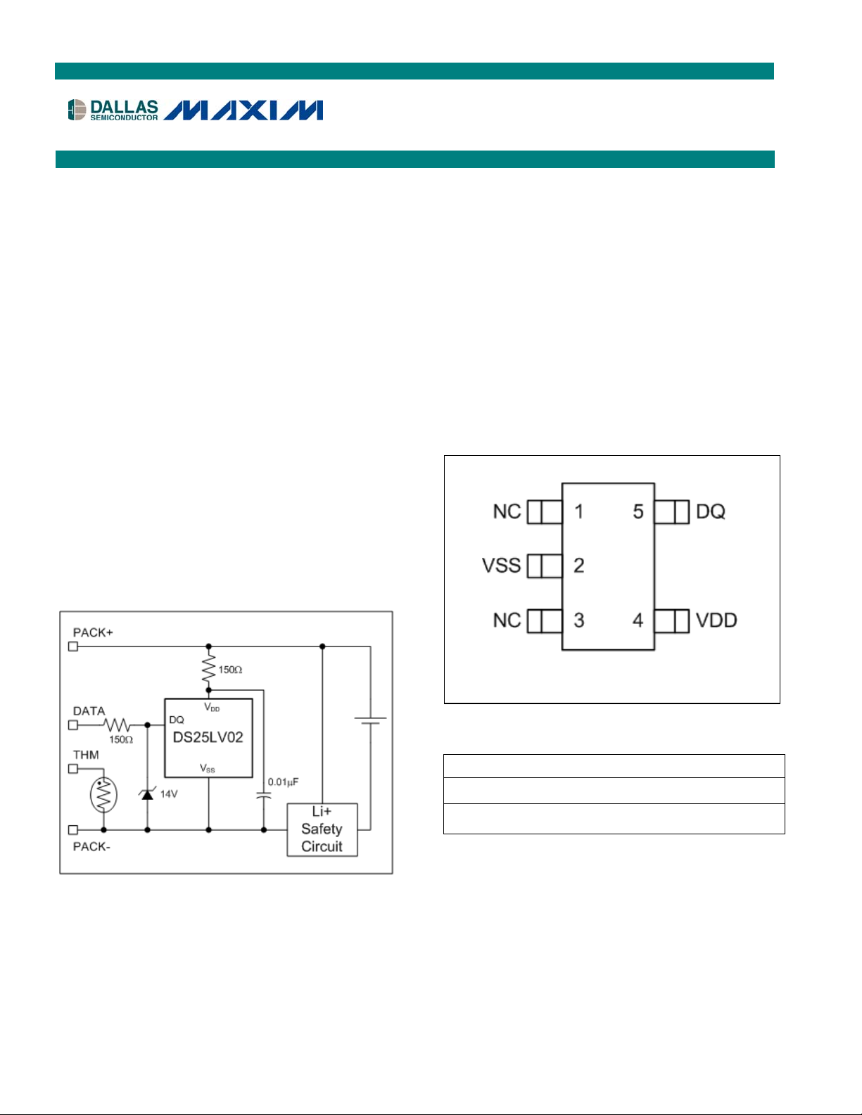
TYPICAL APPLICATION CIRCUIT
DS25LV02
Low-Voltage 1024-Bit EPROM
FEATURES
§ 128 Bytes of EPROM Storage Organized into
Four Separately Lockable Pages
§ Backward-Compatible with DS2502
§ Dallas 1-Wire Interface
§ Input Logic Thresholds Compatible with 1.8V
I/O Supply Rail
§ Unique 64-Bit Serial Number
§ Operates with V
§ Tiny, Thin SOT-23 Package
PIN CONFIGURATION
TOP VIEW
as Low as 2.2V
DD
5-Pin Thin-SOT (TSOT)
ORDERING INFORMATION
PART TEMP RANGE PIN-PACKAGE
DS25LV02R+U
DS25LV02R+T&
R
+Denotes lead-free package.
1-Wire is a registered trademark of Dallas Semiconductor.
Certain commands, modes, and registers are capitalized for
clarity.
-30°C to +85°C
-30°C to +85°C
5 Thin SOT
5 Thin SOT in
Tape-and-Reel
1 of 17 051106
Page 2

DS25LV02: Low-Voltage 1024-Bit EPROM
ABSOLUTE MAXIMUM RATINGS
Voltage Range on DQ, Relative to VSS -0.3V to +12V
Voltage Range on V
, Relative to VSS -0.3V to +6V
DD
Operating Temperature Range -30°C to +85°C
Storage Temperature Range -55°C to +125°C
Soldering Temperature See IPC/JEDEC J-STD-020A Specification
Stresses beyond those listed under “Absolute Maximum Ratings” may cause permanent damage to the device. These are stress ratings only,
and functional operation of the device at these or any other conditions beyond those indicated in the operational sections of the specifications is
not implied. Exposure to the absolute maximum rating conditions for extended periods may affect device.
RECOMMENDED DC OPERATING CONDITIONS
(2.2V £ VDD £ 5.5V, TA = -30°C to +85°C.)
PARAMETER SYMBOL CONDITIONS MIN TYP MAX UNITS
Supply Voltage VDD (Notes 1, 2) 2.2 5.5 V
Data Pin Communication Voltage VDQ (Note 1) -0.3 +5.5 V
Data Pin Programming Voltage VPP (Notes 1, 2, 5) 11.5 12.0 V
DC ELECTRICAL CHARACTERISTICS
(2.2V £ VDD £ 5.5V, TA = -30°C to +85°C.)
PARAMETER SYMBOL CONDITIONS MIN TYP MAX UNITS
I
DQ Idle (Note 4) 0.8 2
Supply Current
DD0
I
Communication mode, DQ active 300
DD1
mA
Input-Logic High: DQ VIH (Note 1) 1.5 V
VDD ≥ 2.5V 0.6
Input-Logic Low: DQ (Note 1) VIL
V
0.4
Output-Logic Low: DQ V
OL
Pulldown Current: DQ IPD 0.5
IOL = 4mA (Note 1) 0.4 V
mA
EPROM RELIABILITY SPECIFICATION
(2.2V £ VDD £ 5.5V, TA = -30°C to +85°C.)
PARAMETER SYMBOL CONDITIONS MIN TYP MAX UNITS
Storage t
(Notes 2, 3) 10 Years
EES
2 of 17
Page 3

DS25LV02: Low-Voltage 1024-Bit EPROM
AC ELECTRICAL CHARACTERISTICS: EPROM PROGRAMMING
(3.0V £ VDD £ 5.5V, TA = -30°C to +50°C.)
PARAMETER SYMBOL CONDITIONS MIN TYP MAX UNITS
Programming Pulse Width t
Program Voltage Rise Time t
PP
RP
(Notes 1, 2, 5, 6) 480 5000
(Notes 1, 2, 5) 0.5 5.0
Program Voltage Fall Time tFP (Notes 1, 2, 5) 0.5 5.0
Programming Current: DQ Pin I
PP
(Notes 2, 5, 7) 6 10 mA
AC ELECTRICAL CHARACTERISTICS: 1-Wire INTERFACE
(2.2V £ VDD £ 5.5V, TA = -30°C to +85°C.)
PARAMETER SYMBOL CONDITIONS MIN TYP MAX UNITS
Time Slot t
Recovery Time t
Write-0 Low Time t
Write-1 Low Time t
Read-Data Valid t
Reset-Time High t
Reset-Time Low t
60 120
SLOT
1
REC
60 120
LOW0
1 15
LOW1
15
RDV
480
RSTH
480 960
RSTL
ms
ms
ms
ms
ms
ms
ms
ms
ms
ms
Presence-Detect High t
Presence-Detect Low t
Delay to Program Pulse tDP 5
Delay to Verify tDV 5
15 60
PDH
60 240
PDL
ms
ms
ms
ms
DQ Capacitance CDQ 50 pF
Note 1:
Note 2:
Note 3:
Note 4:
Note 5:
Note 6:
Note 7:
All voltages are referenced to V
Programming of the EPROM Data and EPROM Status fields require a limited temperature range of 0°C to 50°C and limited V
voltage range of 3.0V to 5.5V.
Storage for t
DQ < V
Programming pulse on DQ pin must be shaped to conform with rise, fall, and width timing specifications. See Figure 7. EPROM
Programming Diagram).
The accumulative duration of all programming pulses for each address must not exceed 5ms.
Specification is guaranteed by design.
at +50°C.
EES
for t > 1.5ms or DQ > VIH for t > 1.5ms [1-Wire oscillator shut down].
IL
.
SS
DD
3 of 17
Page 4
DS25LV02: Low-Voltage 1024-Bit EPROM
PIN DESCRIPTION
PIN NAME FUNCTION
1, 3 N.C. No Connection
2
V
SS
Supply GND and Reference for Serial Communication. Attach
terminal.
V
to battery-pack negative
SS
4
5 DQ
V
DD
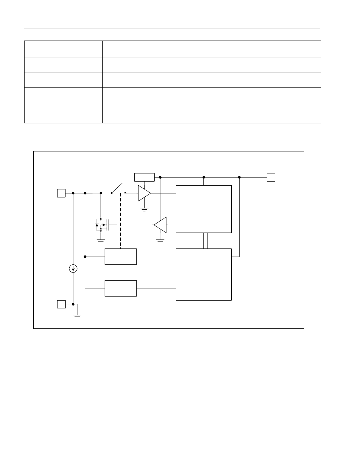
Figure 1. Block Diagram
DQ
HV
0.5mA
Supply Input. Bypass to VSS with 0.01mF (typ).
Serial Interface Data I/O Pin. Bidirectional data transmit and receive at 16kbps. Input for
programming voltage pulse during EPROM programming. Internal 0.5mA pulldown ensures
idle mode is entered when no DQ pullup is present.
VDD
HV Detect
Reg.
Vdd_int
DIN
1-Wire I/F
and
Control
DOUT
EPROM Array
HV Shaper
Vpp
VSS
DETAILED DESCRIPTION
The DS25LV02 provides battery-pack identification and data storage. A 128-byte EPROM memory array and an 8
byte status field accessed by a low-voltage 1-Wire interface. Each DS25LV02 has a unique 64-bit Net Address
(ROM ID) for identification.
The EPROM is divided into four 32-byte pages. An additional 8-byte status field provides lock bit and page
redirection information to the user. EPROM writing occurs one byte at a time by supplying a 12V pulse on the DQ
line in-between each byte written. Each page can be individually locked by clearing the appropriate bit in the Status
field. Data is read sequentially from a starting address through the end of the array. CRC verification provides
integrity of all read and written data.
Functional compatibility has been maintained between the DS2502 and DS25LV02 at the Net Address/ROM
Command and Function Command levels for reading and writing the Memory data and Status data fields.
4 of 17
Page 5

DS25LV02: Low-Voltage 1024-Bit EPROM
EPROM MEMORY DATA FIELD
The DS25LV02 has a linear address space for access to the EPROM data field. The EPROM data field is
organized as 4 pages of 32 bytes each as shown in Table 1. The Read Memory and Read Data/Generate CRC
Memory function commands provide read access to the 1024 bits of the EPROM data field. The Write Memory
function command provides write access to the EPROM data field. When received from the factory, the entire
1024-bit EPROM data field is erased and returns logical 1’s when read. Bits within the data field are one time
programmable. Programming changes the bit value to logical zero from the factory default erased value of a logical
1. Once a bit is programmed, it cannot be set back to a logical 1.
Table 1. EPROM Data Field
ADDRESS (HEX) DESCRIPTION READ/WRITE
0000–001F PAGE 0 (32 bytes) R/W*
0020–003F PAGE 1 (32 bytes) R/W*
0040–005F PAGE 2 (32 bytes) R/W*
0060–007F PAGE 3 (32 bytes) R/W*
0080–FFFF Reserved
* One-time write to “0” for each bit.
READ MEMORY [F0h]
The Read Memory command is used to read data from PAGE 0 to PAGE 3 of the 1024-bit EPROM data field. The
bus master follows the command byte with a 2-byte address (TA1 = (T7:T0), TA2 = (T15:T8)) that indicates a
starting byte location within the data field. An 8-bit CRC of the command byte and address bytes is computed by
the DS25LV02 and read back by the bus master to confirm that the correct command word and starting address
were received. If the CRC is deemed to be incorrect by the bus master, the bus master should issue a reset pulse
and repeat the entire sequence. If the CRC is deemed to be correct by the bus master, read time slots can be
issued to receive data from the EPROM data field starting at the initial address. The bus master can issue a reset
pulse at any point or continue to issue read time slots until the end of PAGE 3 of the data field is reached.
If reading continues through the end of PAGE 3, the bus master can issue eight additional read time slots and the
DS25LV02 will respond with a 8-bit CRC of all data bytes read from the initial starting byte through the last byte of
PAGE 3. Terminating the command transaction with a reset pulse prior to reaching the end of PAGE 3 results in a
loss of availability of the 8-bit CRC.
READ DATA/GENERATE 8-BIT CRC [C3h]
The Read Data/Generate 8-bit CRC command is used to read data from PAGE 0 to PAGE 3 of the 1024-bit
EPROM data field. The bus master follows the command byte with a 2-byte address
(TA1 = (T7:T0), TA2 = (T15:T8)) that indicates a starting byte location within the data field. An 8-bit CRC of the
command byte and address bytes is computed by the DS25LV02 and read back by the bus master to confirm that
the correct command word and starting address were received. If the CRC is deemed to be incorrect by the bus
master, the bus master should issue a reset pulse and repeat the entire sequence. If the CRC is deemed to be
correct by the bus master, read time slots can be issued to receive data from the EPROM data field starting at the
initial address. The bus master can issue a reset pulse at any point or continue to issue read time slots until the
end of the 32-byte page is reached. If reading occurs through the end of the 32-byte page, the bus master can
issue eight additional read time slots and the DS25LV02 will respond with an 8-bit CRC of all data bytes read from
the initial starting byte through the last byte of the current page. After the CRC is received, additional read time
slots return data starting with the first byte of the next page. This sequence will continue until the bus master reads
PAGE 3 and its accompanying CRC. Thus each page of data can be considered to be 33 bytes long: the 32 bytes
of user-programmed EPROM data and an 8-bit CRC that gets generated automatically at the end of each page.
The Read Data/Generate 8-Bit CRC command sequence can be exited at any point by issuing a reset pulse.
5 of 17
Page 6

DS25LV02: Low-Voltage 1024-Bit EPROM
WRITE MEMORY [0Fh]
The Write Memory command is used to program the 1024-bit EPROM data field. Programming is performed one or
more bytes at a time, with CRCs of the master-to-slave bit stream provided for data integrity. To begin a memory
write, the bus master issues the Write Memory function command followed by a 2-byte address argument
(TA1 = (T7:T0), TA2 = (T15:T8)) and a 1-byte data argument (D7:D0). The 2-byte address argument sets the
starting byte position in the EPROM data field of the first byte to be written. The data argument provides data for
the first byte to be written. The master must issue 8 read timeslots following the data argument.
An 8-bit CRC of the command byte, address bytes and data byte computed by the DS25LV02 is returned in the 8
timeslots to enable the master to check the integrity of the communication. If the CRC is deemed to be incorrect by
the bus master, the bus master should issue a reset pulse and repeat the entire sequence. If the CRC is deemed to
be correct by the bus master, a programming pulse can be issued to program the byte position within the EPROM
data field pointed to by T15:T0. Following the programming pulse, the bus master must issue 8 read timeslots. The
read timeslots return the EPROM data byte value (least significant bit first) for confirmation by the master.
The bus master can issue a reset pulse at any point after issuing the program pulse to end the write operation, or
continue the write operation with the next byte in the EPROM data field. If a the write operation is continued, the
DS25LV02 automatically increments the internal address pointer to select the next byte in the EPROM data field,
and the new value of T7:T0 is loaded into the 8-bit CRC generator as the starting value. The bus master issues the
next 1-byte data argument followed by 8 read timeslots to return the CRC computed by the DS25LV02. The value
returned is computed with D7:D0, using T7:T0 as the starting value. If the CRC is deemed to be incorrect by the
bus master, the bus master should issue a reset pulse and repeat the entire sequence. If the CRC is deemed to be
correct by the bus master, a programming pulse can be issued to program the byte position pointed to by T15:T0.
Following the programming pulse, the bus master must issue 8 read timeslots. The read timeslots return the
EPROM data byte value (least significant bit first) for confirmation by the master.
The write operation can be continued until the end of the EPROM data field is reached by repeating the sequence
of issuing a 1-byte data argument, 8 read timeslots to return CRC, a programming pulse, and 8 read timeslots to
return EPROM data.
EPROM STATUS
The DS25LV02 has a separate 8-byte linear address space for access to the EPROM STATUS data field using the
Read Status and Write Status function commands.
READ STATUS [AAh]
The Read Status command is used to read data from the EPROM Status data field. The bus master follows the
command byte with a 2-byte address (TA1 = (T7:T0), TA2 = (T15:T8)) that indicates a starting byte location within
the data field. An 8-bit CRC of the command byte and address bytes is computed by the DS25LV02 and read back
by the bus master to confirm that the correct command word and starting address were received. If the CRC is
deemed to be incorrect by the bus master, a reset pulse should be issued and the entire sequence repeated. If the
CRC is deemed to be correct by the bus master, read timeslots can be issued to receive data starting at the initial
address. The bus master can issue a reset pulse at any point or continue to issue read timeslots until the end of
the EPROM Status data field is reached. If reading occurs through the end of the EPROM Status data field, the bus
master can issue 8 additional read timeslots and the DS25LV02 will respond with a 8-bit CRC of all data bytes read
from the initial starting byte through the last byte. Additional read timeslots return logical 1s until the internal
address reaches a multiple of 128. Then data is returned from address 0000h. The Read Status command
sequence can be ended at any point by issuing a reset pulse.
WRITE STATUS [55h]
The Write Status command is used to program the EPROM status field. To begin a status field write, the bus
master issues the Write Status function command followed by a 2-byte address argument
(TA1 = (T7:T0), TA2 = (T15:T8)) and a 1-byte data argument (D7:D0). The 2-byte address argument sets the
starting byte position in the EPROM status field of the first byte to be written. The data argument provides data for
the first byte to be written. The master must issue 8 read timeslots following the data argument.
An 8-bit CRC of the command byte, address bytes, and data byte computed by the DS25LV02 is returned in the 8
timeslots to enable the master to check the integrity of the communication. If the CRC is deemed to be incorrect by
the bus master, the bus master should issue a reset pulse and repeat the entire sequence. If the CRC is deemed to
6 of 17
Page 7

DS25LV02: Low-Voltage 1024-Bit EPROM
be correct by the bus master, a programming pulse can be issued to program the byte position within the EPROM
status field pointed to by T15:T0. Following the programming pulse, the bus master must issue 8 read timeslots.
The read timeslots return the EPROM status byte value (least significant bit first) for confirmation by the master.
The bus master can issue a reset pulse at any point after issuing the program pulse to end the write operation, or
continue the write operation with the next byte in the EPROM status field. If the write operation is continued, the
DS25LV02 automatically increments the internal address pointer to select the next byte in the EPROM status field,
and the new value of T7:T0 is loaded into the 8-bit CRC generator as the starting value. The bus master issues the
next 1-byte data argument followed by 8 read timeslots to return the CRC computed by the DS25LV02. The value
returned is computed with D7:D0, using T7:T0 as the starting value. If the CRC is deemed to be incorrect by the
bus master, the bus master should issue a reset pulse and repeat the entire sequence. If the CRC is deemed to be
correct by the bus master, a programming pulse can be issued to program the byte position pointed to by T15:T0.
Following the programming pulse, the bus master must issue 8 read timeslots. The read timeslots return the
EPROM status byte value (least significant bit first) for confirmation by the master.
The write operation can be continued until the end of the EPROM status field is reached by repeating the sequence
of issuing a 1-byte data argument, 8 read timeslots to return CRC, a programming pulse, and 8 read timeslots to
return EPROM byte value.
Table 2. EPROM Status Field
ADDRESS (HEX) DESCRIPTION READ/WRITE
Write Protect Page bits
B0: Page 0 Write Protect
B1: Page 1 Write Protect
B2: Page 2 Write Protect
0000
B3: Page 3 Write Protect
B4: Reserved for TMEX
B5: Reserved for TMEX
B6: Reserved for TMEX
B7: Reserved for TMEX
R/W*
0001 Page Redirection Byte for Page 0 R/W*
0002 Page Redirection Byte for Page 1 R/W*
0003 Page Redirection Byte for Page 2 R/W*
0004 Page Redirection Byte for Page 3 R/W*
0005-0006 Reserved R
0007 Factory Programmed to 00h R
* One-time write to “0” for each bit.
7 of 17
Page 8

DS25LV02: Low-Voltage 1024-Bit EPROM
Table 3. EPROM Memory and Status Function Commands
COMMAND HEX FUNCTION
Read data from the lower 1024 bits of the 1024-bit EPROM Memory
Read Memory F0
Read Data/Generate CRC C3
Write Memory 0F Write data to the EPROM data field.
data field. Generates a CRC value if a read continues through the
end of the last page.
Read data from the lower 1024 bits of the 1024-bit EPROM Memory
data field. Generates a CRC value of the data if read continues
through the end of the page.
Read Status AA
Write Status 55
Note: The Write Memory, Read Memory, Read Data/Generate CRC, Write Status, and Read Status commands
filter the target address (TA2:TA1) value with a 007Fh AND mask that limits the addressable size of the EPROM
data field and EPROM status field to 1024 bits. Target address values equal to or greater than 0080h (128 decimal)
return data from the lower 128 bytes of the respective data field. The result of the filtering is that the internal
address wraps around every 128 bytes as the external target address increments in multiples of 128. For instance,
each time a read operation crosses a 128-byte boundary (0080h, 0100h, … FF00h, FF80h) data retrieval begins
again at address 0000h. This process repeats until reading occurs through the end of the 64kb memory space
addressable by T15:T0. It is also important to note that the filter is applied prior to calculation of the CRC, so that
target address values that are multiples of 128 return the same CRC. The CRC values should be considered
correct only for T15:T0 in the range of 0000h to 007Fh.
Read data from the 8-byte EPROM status field. Generates a CRC if
read continues through the end of the field.
Write the Page Protection bits and Page Redirection bytes in the
EPROM status field.
1-Wire BUS SYSTEM
The 1-Wire bus is a system that has a single bus master and one or more slaves. A multidrop bus is a 1-Wire bus
with multiple slaves, while a single-drop bus has only one slave device. In all instances, the DS25LV02 is a slave
device. The bus master is typically a microprocessor in the host system. The discussion of this bus system consists
of five topics: 64-bit net address, CRC generation, hardware configuration, transaction sequence, and 1-Wire
signaling.
64-BIT NET ADDRESS (ROM ID)
Each DS25LV02 has a unique, factory-programmed 1-Wire Net Address that is 64 bits in length. The term Net
Address is synonymous with the ROM ID or ROM Code terms used in the DS2502 and older Dallas 1-Wire
documentation. The first 8 bits of the Net Address are the 1-Wire family code (09h for the standard DS25LV02).
The next 48 bits are a unique serial number. The last 8 bits are a cyclic redundancy check (CRC) of the first 56 bits
(see Figure 2). The 64-bit net address and the 1-Wire I/O circuitry built into the device enable the DS25LV02 to
communicate through the 1-Wire protocol detailed in this data sheet.
Figure 2. 1-Wire Net Address Format
8-BIT CRC 48-BIT SERIAL NUMBER
MSb LSb
8-BIT FAMILY
CODE (09H)
8 of 17
Page 9

DS25LV02: Low-Voltage 1024-Bit EPROM
CRC GENERATION
The DS25LV02 has an 8-bit CRC stored in the most significant byte of its 1-Wire net address and generates a CRC
during some command protocols. To ensure error-free transmission of the address, the host system can compute a
CRC value from the first 56 bits of the address and compare it to the CRC from the DS25LV02.
The host system is responsible for verifying the CRC value and taking action as a result. The DS25LV02 does not
compare CRC values and does not prevent a command sequence from proceeding as a result of a CRC mismatch.
Proper use of the CRC can result in a communication channel with a very high level of integrity.
The CRC can be generated by the host using a circuit consisting of a shift register and XOR gates as shown in
Figure 3, or it can be generated in software using the polynomial X
Dallas 1-Wire CRC is available in Application Note 27: Understanding and Using Cyclic Redundancy Checks with
Dallas Semiconductor i
In the circuit in Figure 3, the shift register bits are initialized to 0. Then, starting with the least significant bit of the
family code, one bit at a time is shifted in. After the 8th bit of the family code has been entered, then the serial
number is entered. After the 48th bit of the serial number has been entered, the shift register contains the CRC
value.
ButtonÒ Products (www.maxim-ic.com/appnoteindex).
8
+ X5 + X4 + 1. Additional information about the
Figure 3. 1-Wire CRC Generation Block Diagram
INPUT
MSb
XOR
XOR
LSb
XOR
During some command sequences, the DS25LV02 also generates an 8-bit CRC and provides this value to the bus
master to facilitate validation for the transfer of command, address, and data from the bus master to the
DS25LV02. The DS25LV02 computes an 8-bit CRC for the command and address bytes received from the bus
master for the Read Memory, Read Status and Read/Generate CRC commands to confirm that these bytes have
been received correctly. The CRC generator on the DS25LV02 is also used to provide verification of error-free data
transfer as each EPROM page is sent to the master during a Read Data/Generate CRC command and for the 8
bytes of information in the Status memory field.
In each case where a CRC is used for data transfer validation, the bus master must calculate the CRC value using
the same polynomial function and compare the calculated value to the CRC either stored in the DS25LV02 Net
Address or computed by the DS25LV02. The comparison of CRC values and decision to continue with an
operation are determined entirely by the bus master. There is no circuitry in the DS25LV02 that prevents the
command sequence from proceeding if the stored or calculated CRC from the DS25LV02 and the calculated CRC
from the host do not match.
HARDWARE CONFIGURATION
Because the 1-Wire bus has only a single line, it is important that each device on the bus be able to drive it at the
appropriate time. To facilitate this, each device attached to the 1-Wire bus must connect to the bus with open-drain
or tri-state output drivers. The DS25LV02 uses an open-drain output driver as part of the bidirectional interface
circuitry shown in Figure 4. If a bidirectional pin is not available on the bus master, separate output and input pins
can be connected together.
The 1-Wire bus must have a pullup resistor at the bus-master end of the bus. A value between 2kW and 5kW is
recommended. The idle state for the 1-Wire bus is high. If, for any reason, a bus transaction must be suspended,
the bus must be left in the idle state to properly resume the transaction later. Note that if the bus is left low for more
iButton is a registered trademark of Dallas Semiconductor.
9 of 17
Page 10

than t
, slave devices on the bus begin to interpret the low period as a reset pulse, effectively terminating the
LOW0
transaction.
Figure 4. 1-Wire Bus Interface Circuitry
Vpullup
(1.8 to 5.5V)
DS25LV02: Low-Voltage 1024-Bit EPROM
Bus Master
Rx
Tx
4.7kW
Rx = Receive
Tx = Transmit
Device 1-Wire Port (DQ)
~100 Ohm
MOSFET
~0.5µA
Rx
Tx
TRANSACTION SEQUENCE
The protocol for accessing the DS25LV02 through the 1-Wire port is as follows:
§ Initialization
§ Net Address Command
§ Function Command(s)
§ Data Transfer
All transactions of the 1-Wire bus begin with an initialization sequence consisting of a reset pulse transmitted by the
bus master, followed by a presence pulse simultaneously transmitted by the DS25LV02 and any other slaves on
the bus. The presence pulse tells the bus master that one or more devices are on the bus and ready to operate.
For more details, see below.
NET ADDRESS COMMANDS
Once the bus master has detected the presence of one or more slaves, it can issue one of the net address
commands described in the following paragraphs. The name of each Net Address command (ROM command) is
followed by the 8-bit opcode for that command in square brackets.
Read Net Address [33h]. This command allows the bus master to read the DS25LV02’s 1-Wire net address. The
bus master follows the Read Net Address command with 64 read timeslots allowing the 1-Wire slave to transmit its
address. This command can only be used if there is a single slave on the bus. If more than one slave is present, a
data collision occurs when all slaves try to transmit at the same time (open drain produces a wired-AND result).
Match Net Address [55h]. This command allows the bus master to specifically address one DS25LV02 on the
1-Wire bus. Following this command, the bus master transmits the 64 bit net address of the desired slave device.
Only the addressed DS25LV02 responds to any subsequent function command. All other slave devices ignore the
function command and wait for a reset pulse. This command can be used with one or more slave devices on the
bus.
Skip Net Address [CCh]. This command saves time when there is only one DS25LV02 on the bus by allowing the
bus master to issue a function command without specifying the address of the slave. If more than one slave device
is present on the bus, a subsequent function command can cause a data collision when all slaves transmit data at
the same time.
Search Net Address [F0h]. This command allows the bus master to use a process of elimination to identify the
1-Wire net addresses of all slave devices on the bus. The search process involves the repetition of a simple three-
10 of 17
Page 11

DS25LV02: Low-Voltage 1024-Bit EPROM
step routine: read a bit, read the complement of the bit, then write the desired value of that bit. The bus master
performs this simple three-step routine on each bit location of the net address. After one complete pass through all
64 bits, the bus master knows the address of one device. The remaining devices can then be identified on
additional iterations of the process. Refer to Chapter 5 of the Book of DS19xx i
comprehensive discussion of a net address search, including an actual example (www.maxim-ic.com/iButtonBook
Button Standards for a
).
I/O SIGNALING
The 1-Wire bus requires strict signaling protocols to ensure data integrity. The four protocols used by the
DS25LV02 are as follows: the initialization sequence (reset pulse followed by presence pulse), write 0, write 1, and
read data. The bus master initiates all these types of signaling except the presence pulse.
The initialization sequence required to begin any communication with the DS25LV02 is shown in Figure 5. A
presence pulse following a reset pulse indicates that the DS25LV02 is ready to accept a net address command.
The bus master transmits (Tx) a reset pulse for t
. The bus master then releases the line and goes into receive
RSTL
mode (Rx). The 1-Wire bus line is then pulled high by the pullup resistor. After detecting the rising edge on the DQ
pin, the DS25LV02 waits for t
and then transmits the presence pulse for t
PDH
PDL
.
Figure 5. 1-Wire Initialization Sequence
DQ
LINE TYPE LEGEND:
t
RSTL
t
PDH
t
PDL
t
RSTH
PACK+
PACK-
BOTH BUS MASTER AND
SLAVE ACTIVE LOW
WRITE-TIME SLOTS
A write-time slot is initiated when the bus master pulls the 1-Wire bus from a logic-high (inactive) level to a logic-low
level. There are two types of write-time slots: write 1 and write 0. All write-time slots must be t
a 1ms minimum recovery time, t
and t
LOW0_MIN
after the line falls. If the line is high when sampled, a write 1 occurs. If the line is low when sampled, a
, between cycles. The DS25LV02 samples the 1-Wire bus line between t
REC
in duration with
SLOT
LOW1_MAX
write 0 occurs. The sample window is illustrated in Figure 6. For the bus master to generate a write-1 time slot, the
bus line must be pulled low and then released, allowing the line to be pulled high less than t
after the start of the
RDV
write time slot. For the host to generate a write-0 time slot, the bus line must be pulled low and held low for the
duration of the write-time slot.
READ-TIME SLOTS
A read-time slot is initiated when the bus master pulls the 1-Wire bus line from a logic-high level to a logic-low level.
The bus master must keep the bus line low for at least 1ms and then release it to allow the DS25LV02 to present
valid data. The bus master can then sample the data t
read-time slot, the DS25LV02 releases the bus line and allows it to be pulled high by the external pullup resistor. All
read-time slots must be t
in duration with a 1ms minimum recovery time, t
SLOT
the timing specifications in the Electrical Characteristics table for more information.
from the start of the read-time slot. By the end of the
RDV
, between cycles. See Figure 6 and
REC
11 of 17
Page 12

Figure 6. 1-Wire Write and Read Time Slots
WRITE 0 SLOT WRI TE 1 SLOT
DS25LV02: Low-Voltage 1024-Bit EPROM
V
PULLU P
GND
MODE
Standard
Overdrive
V
PULLU P
15ms
2ms
t
RDV
t
SLOT
t
LOW0
t
Device Sample Window
MIN TYP MAX
15ms 30ms
1ms 3ms
Data = 0
t
SLOT
REC
>1ms
15ms
2ms
READ DATA SLOT
t
REC
t
RDV
t
SLOT
t
LOW1
Device Sample Window
MIN T YP MAX
15ms 30ms
1ms 3ms
Data = 1
t
SLOT
GND
>1ms
Master Sample Window
15ms
MODE
Standard
Overdrive
Master Sampl e Wi ndow
15ms
2ms 2ms
LINE TYPE LEGEND:
Bus Master active LOW Slave Device active LOW
Both Bus Master and Slave Device Resistor pullup
active LOW
12 of 17
Page 13

Figure 7. EPROM Programming Diagram
DS25LV02: Low-Voltage 1024-Bit EPROM
t
RP
VPP Min = 11.5V,
VPP Max = 12.0V
t
DP
1-Wire
Reset
SKIP ROM
Command
Write
Memory
TA1, TA2, Data
and CRC bytes
Programming
Pulse
Command
Presence
Pulse
PACKAGE INFORMATION
(For the latest package outline information, go to www.maxim-ic.com/DallasPackInfo.)
t
PP
t
FP
t
DV
Verification
Read
13 of 17
Page 14

Figure 8. Operational Flow Chart
START
MASTER T x
RESET PULSE
DS25LV02 Tx
PRESENCE PULSE
MASTER Tx
NET ADDRESS
COMMAND
DS25LV02: Low-Voltage 1024-Bit EPROM
33h/39h
READ
DS25LV0 2 Tx
FAMILY CODE
1 BYTE
DS25LV0 2 Tx
SERIAL NUMBER
6 BYTES
DS25LV0 2 Tx
CRC
1 BYTE
NO
55h
MATCH
YES
MAST ER Tx
BIT 0
BIT 0
MATCH?
YES
MAST ER Tx
BIT 1
BIT 1
MATCH?
YES
NO NO
F0h
SEARCH
YESYES
DS25 LV02 Tx BIT 0
DS25 LV02 Tx BIT 0
MASTER Tx BI T 0
NO
NO
BIT 0
MATCH?
DS25 LV02 Tx BIT 1
DS25 LV02 Tx BIT 1
MASTER Tx BI T 1
NO NO
BIT 1
MATCH?
YES
CCh
SKIP
YES
GO TO MEMOR Y
COMMANDS 1
NO
DS25LV02 Tx BIT 63
DS25LV02 Tx BIT 63
MAST ER Tx BIT 63
GO TO MEMORY
COMMANDS 1
YES
MAST ER Tx
BIT 63
BIT 63
MATCH?
NO
GO TO START
14 of 17
Page 15

Figure 8. Operational Flow Chart (Continued)
MEMORY
COMMANDS 1
MASTER Tx MEMORY
FUNCTION COMMAND
DS25LV02: Low-Voltage 1024-Bit EPROM
BUS MASTER Rx 8-BIT CRC OF
COMMAND AND ADDRESS
DS25LV02 INCREMENTS
ADDRESS COUNTER
NO
F0h
READ
MEMORY
?
YES
BUS MASTER T x
TA1 (T7:T0)
BUS MASTER T x
TA2 (T15:T8)
CRC
CORRECT
?
YES
BUS MASTER Rx DATA
FROM DATA MEMORY
BUS MASTER
Tx RESET
?
NO
END
OF D AT A
MEMORY
?
YES
NO
NO
YES
BUS MASTER T x
RESET
AAh
READ
STAT US
?
YES
BUS MASTER T x
TA1 (T7:T0)
BUS MASTER T x
TA2 (T15:T8)
BUS MASTER Rx 8-BIT CRC OF
COMMAND AND ADDRESS
NO
BUS MASTER Rx DATA
FROM STATUS MEMORY
YES
CRC
CORRECT
?
YES
BUS MASTER
Tx RESET
?
NO
END OF
PAGE
?
YES
NO
DS25LV02 INCREMENTS
ADDRESS COUNTER
NO
GO TO MEMORY
COMMANDS 2
BUS MASTER
Tx RESET
?
NO
BUS MASTER Rx 8-BIT
CRC OF DATA
BUS MASTER
Tx RESET
?
NO
BUS MASTER Rx
ALL 1's
YES
YES
DS25LV02 Tx
PRESENCE PULSE
GO TO ST ART
YES
BUS MASTER
Tx RESET
?
NO
BUS MASTER R x 8-BIT
CRC OF STATUS DATA
YES
BUS MASTER
Tx RESET
?
NO
BUS MASTER Rx
ALL 1's
15 of 17
Page 16

Figure 8. Operational Flow Chart (Continued)
DS25LV02: Low-Voltage 1024-Bit EPROM
MEMORY
COMMANDS 2
DS25LV02 INCREMENTS
ADDRESS COUNTER
C3h
READ DAT A
& GENERATE
CRC ?
YES
BUS MASTER Tx
TA1 (T7:T0)
BUS MASTER Tx
TA2 (T15:T8)
BUS MASTER Rx 8-BIT CRC OF
COMMAND AND ADDRESS
CRC
CORRECT
?
BUS MASTER Rx DAT A
FROM DATA MEMORY
BUS MASTER
Tx RESET
?
NO
NO
YES
YES
NO
GO TO MEMORY
COMMANDS 3
BUS MASTER T x
RESET
END OF
NO
NO
PAGE
?
YES
BUS MASTER R x 8-BIT
CRC OF STATUS DATA
CRC
CORRECT
?
YES
END OF
MEMORY
?
YES
BUS MASTER
Tx RESET
?
NO
BUS MASTER Rx
ALL 1's
NO
YES
BUS MASTER T x
RESET
DS25LV02 Tx
PRESENCE PULSE
GO TO START
16 of 17
Page 17

Figure 8. Operational Flow Chart (Continued)
DS25LV02: Low-Voltage 1024-Bit EPROM
MEMORY
COMMANDS 3
0Fh
WRITE
MEMORY
?
BUS MASTER T x
TA1 (T7:T0)
BUS MASTER T x
TA2 (T15:T8)
BUS MASTER T x
DATA BYTE (D7:D0)
BUS MASTER Rx 8-BIT CRC OF
COMMAND, ADDRESS, AND DATA
CRC OF ADDRESS AND DATA
NO
st
PASS )
(1
(SUBSEQU ENT PASSES)
CRC
CORRECT
?
BUS MASTER T x
PROGRAM PULSE
NO
YES
YES
55h
WRITE
STATUS
?
BUS MASTER T x
TA1 (T7:T0)
BUS MASTER T x
TA2 (T15:T8)
BUS MASTER T x
DATA BYTE (D7:D0)
BUS MAST ER R x CRC16 OF
COMMAND, ADDRESS, AND DATA
CRC16 OF ADDRESS AND DATA
NO
st
PASS)
(1
(SUBSEQUENT PASSES)
CRC
CORRECT
?
BUS MASTER T x
PROGRAM PULSE
NO
YES
YES
BUS MASTER
TX RESET
BUS MAST ER
TX RESET
DS25LV02 COPIES
SCRATCHPAD TO DATA EPROM
BUS MAST ER Rx BYTE
NO
YES
DS25LV02 INCREMENTS
ADDRESS COUNTER
DS25LV02 LOADS LSB OF
NEW ADDRESS INTO CRC
NO
FROM EPROM
EPROM BYT E
= CORRECT
?
YES
END OF
DATA
MEMORY
?
NO
GENE RATOR
BUS MAST ER
TX RESET
DS25LV02 COPIES SCRATCHPAD
TO ST ATU S EPROM
BUS MAST ER R x BYTE
NO
YES
DS25LV02 INCREMENTS
ADDRESS COUNTER
DS25LV02 LOADS LSB OF
NEW ADDRESS INTO CRC
NO
FROM EPROM
EPROM BYTE
= CORR ECT
?
YES
END OF
STATUS
MEMORY
?
NO
GENERATOR
DS25LV02 Tx
PRESEN CE PULSE
GO TO ST ART
17 of 17
 Loading...