

Page 1
www.maxim-ic.com
DS2431
1024-Bit 1-Wire EEPROM
GENERAL DESCRIPTION
The DS2431 is a 1024-bit, 1-Wire® EEPROM chip
organized as four memory pages of 256 bits each.
Data is written to an 8-b yte scratchpad, verif ied, and
then copied to the EEPROM memory. As a special
feature, the four memory pages can individually be
write protected or put in EPROM-emulation mode,
where bits can only be changed from a 1 to a 0 stat e.
The DS2431 communicates over the singleconductor 1-Wire bus. The communication follows
the standard Dallas Semiconductor 1-Wire protocol.
Each device has its own unaltera ble and unique 64bit ROM registration number that is factory lasered
into the chip. The registration number is used to
address the device in a multidrop 1-Wire net
environment.
APPLICATIONS
Accessory/PC Board Ident if ic ati on
Medical Sensor Calibration Data Storage
Analog Sensor Calibration Including IEEEP1451.4 Smart Sensors
Ink and Toner Print Cartridge Identification
After-Market Management of Consumables
FEATURES
!
1024 Bits of EEPROM Memory Partitioned into
Four Pages of 256 Bits
!
Individual Memor y Pages can be Permanently
Write Protected or Put in EPROM-Emulation
Mode ("Write to 0")
!
Switchpoint Hysteresis and Filtering to Optimize
Performance in the Presence of Noise
!
IEC 1000-4-2 Level 4 ESD Protection (8kV
Contact, 15kV Air)
!
Reads and Writes Over a Wide Voltage Range of
2.8V to 5.25V from -40°C to +85°C
!
Communicates to Host with a Single Digital
Signal at 15.4kbps or 111kbps Using 1-Wire
Protocol
ORDERING INFORMATION
PART TEMP RANGE PIN-PACKAGE
DS2431 -40°C to 85°C TO-92
DS2431/T&R -40°C to 85°C TO-92, tape & reel
DS2431P -40°C to 85°C TSOC
DS2431P/T&R -40°C to 85°C TSOC, tape & reel
DS2431X -40°C to 85°C CSP, tape & reel
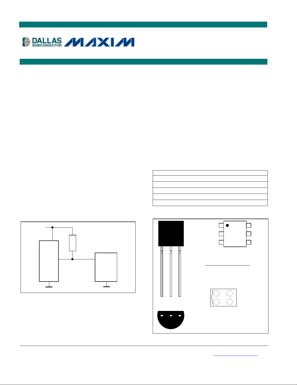
TYPICAL OPERATING CIRCUIT
V
CC
R
PUP
µC
I/O
DS2431
GND
Commands, Registers, and Modes ar e capita li ze d for
clarity.
PIN CONFIGURATION
1
TO-92
1 2 3
1 2 3
2
3
TSOC, TO-92 pi nout:
Pin 1 ------------- GND
Pin 2 ------------- I/O
All other pins -- NC
2
1
A B
CSP, approx. 68 × 68 mil
TSOC, Top View
A1 = NC
A2 = I/O
B1 = NC
B2 = GND
6
5
4
Top view, bumps not visible
1-Wire is a registered trademark of Dallas Semiconductor Corp.
Note: Some revisions of this device may incorporate deviations from published spec ifications known as errata. Multiple revisions of any device
may be simultaneously available through various sales channels. For informati on about device errata, click here: www.maxim-ic.com/errata.
1 of 23
REV: 050704
Page 2

DS2431: 1024-Bit, 1-Wire EEPRO M
ABSOLUTE MAXIMUM RATINGS
I/O Voltage to GND -0.5V, +6V
I/O Sink Current 20mA
Operating Temperature Range -40°C to +85°C
Junction Temperature +150°C
Storage Temperature Range -40°C to +85°C
Soldering Temperature See IPC/JEDEC J-STD-020A
Stresses beyond those listed under “Absolute Maximum Ratings” may caus e permanent damage to the device. These are stress ratings only,
and functional operation of the device at these or any other conditions beyond those indicated in the operational sections of t he specifications is
not implied. Exposure to the absolute maximum rating conditions for extended periods may affect device rel i abili ty .
ELECTRICAL CHARACTERISTICS
(V
= 2.8V to 5.25V, TA = -40°C to +85°C.)
PUP
PARAMETER SYMBOL CONDITIONS MIN TYP MAX UNITS
I/O PIN GENERAL DATA
1-Wire Pullup Resistance
Input Capacitance C
Input Load Current I
High-to-Low Switching
Threshold
Input Low Voltage V
Low-to-High Switching
Threshold
Switching Hysteresis V
Output Low Voltage V
Recovery Time
(Notes 1,11)
Rising-Edge Hold-off Time t
Timeslot Duration (Note 1) t
R
V
V
t
REC
REH
SLOT
PUP
IO
L
TL
IL
TH
HY
OL
I/O PIN, 1-WIRE RESET, PRESENCE DETECT CYCLE
Reset Low Time (Note 1) t
Presence Detect High
Time
Presence Detect Fall Time
(Notes 4, 14)
Presence Detect Low
Time
Presence Detect Sample
Time (Note 1)
RSTL
t
PDH
t
FPD
t
PDL
t
MSP
(Notes 1, 2)
0.3 2.2
kΩ
(Notes 3, 4) 100 800 pF
I/O pin at V
PUP
0.05 2.2 µA
(Notes 4, 5, 6) 0.5 4.1 V
(Notes 1, 7) 0.3 V
(Notes 4, 5, 8) 1.0 4.9 V
(Notes 4, 5, 9) 0.22 1.70 V
At 4mA (Note 10) 0.4 V
Standard speed, R
Overdrive speed, R
PUP
PUP
= 2.2kΩ
= 2.2kΩ
Overdrive speed, directly prior to reset
pulse; R
PUP
= 2.2kΩ
Standard speed (Note 12) 0.5 5.0
Overdrive speed Not applicable (0)
Standard speed 65
Overdrive speed (Note 13) 9
Standard speed, V
> 4.5V 480 640
PUP
Standard speed (Note 12) 504 640
Overdrive speed, V
> 4.5V 48 80
PUP
5
2
µs
5
µs
µs
µs
Overdrive speed (Note 13) 53 80
Standard speed, V
Standard speed (Note 13) 15 63
> 4.5V 15 60
PUP
µs
Overdrive speed (Note 13) 2 7
Standard speed, V
Standard speed 1.1 7
> 4.5V 1.1 3.75
PUP
µs
Overdrive speed 1.1
Standard speed 60 240
Overdrive speed, V
> 4.5V 8 24
PUP
µs
Overdrive speed (Note 13) 8 26
Standard speed, V
Standard speed 70 75
> 4.5V 64 75
PUP
µs
Overdrive speed 8.1 10
2 of 23
Page 3
DS2431: 1024-Bit, 1-Wire EEPRO M
PARAMETER SYMBOL CONDITIONS MIN TYP MAX UNITS
I/O PIN, 1-Wire WRITE
Write-0 Low Time (Note 1) t
Write-1 Low Time
(Notes 1, 15)
I/O PIN, 1-Wire READ
Read Low Time
(Notes 1, 16)
Read Sample Time
(Notes 1, 16)
EEPROM
Programming Current I
Programming Time t
Write/Erase Cycles
(Endurance)
Data Retention t
W0L
t
W1L
t
RL
t
MSR
PROG
PROG
N
CY
DR
Standard speed 60 120
Overdrive speed (Note 13) 716
Standard speed 5
Overdrive speed 1
Standard speed 5
Overdrive speed 1
Standard speed
Overdrive speed
tRL + δ
tRL + δ
15 - ε
2 - ε
15 - δ
2 - δ
15
(Note 17) 1 mA
(Note 18) 12.5 ms
At 25°C 200k
At 85°C (worst case) 50k
At 85°C (worst case) 10 years
µs
µs
µs
2
µs
---
Note 1:
Note 2:
Note 3:
Note 4:
Note 5:
Note 6:
Note 7:
Note 8:
Note 9:
Note 10:
Note 11:
Note 12:
Note 13:
Note 14:
Note 15:
Note 16:
Note 17:
Note 18:
System requirement.
Maximum allowable pullup resistance is a function of the number of 1-Wire devices in the system and 1-Wire recovery times. The
specified value here applies to systems with only one device and with the minimum 1-Wire recovery times. For more heavily
loaded systems, an active pullup such as that found in the DS2482-x00, DS2480B, or DS2490 may be required.
Capacitance on the data pin could be 800pF when V
after V
Guaranteed by design, simulation only. Not production tested.
V
Voltage below which, during a falling edge on I/O, a logic 0 is detected.
The voltage on I/O needs to be less or equal to V
Voltage above which, during a rising edge on I/O, a logic 1 is detected.
After V
The I-V characteristic is linear for voltages less than 1V.
Applies to a single DS2431 attached to a 1-Wire line.
The earliest recognition of a negative edge is possible at t
Highlighted numbers are NOT in compliance with legacy 1-Wire product standards. See comparis on table bel ow.
Interval during the negative edge on I/O at the beginning of a Presence Detect pulse between the time at which the voltage is
80% of V
ε represents the time required for the pullup circuitry to pull the voltage on I/O up from V
δ represents the time required for the pullup circuitry to pull the voltage on I/O up from V
master.
Current drawn from I/O during the EEPROM programming interval. The pullup circuit on I/O during the programming interval
should be such that the voltage at I/O is greater than or equal to Vpup(min). If Vpup in the system is close to Vpup(min) then a
low impedance bypass of Rpup which can be activated during programming may need to be added.
Interval begins t
sequence. Interval ends once the device's self-timed EEPROM programm ing cycle is complete and the current drawn by the
device has returned from I
has been applied the parasite capacitance will not affect normal communications.
PUP
, VTH, and V
TL
TH
are a function of the internal supply voltage.
HY
is crossed during a rising edge on I/O, the voltage on I/O has to drop by at least VHY to be detected as logic '0'.
and the time at which the voltage is 20% of V
PUP
after the leading negative edge on IO for the last timeslot of the E/S byte for a valid Copy Scratchpad
WiLMIN
to IL.
PROG
is first applied. If a 2.2kΩ resistor is used to pull up the data line, 2.5µs
PUP
whenever the master drives the line low.
ILMAX
after VTH has been previously reached.
REH
.
PUP
to VTH.
IL
to the input high threshold of the bus
IL
LEGACY VALUES DS2431 VALUES
PARAMETER STANDARD SPEED OVERDRIVE SPEED STANDARD SPEED OVERDRIVE SPEED
MIN MAX MIN MAX MIN MAX MIN MAX
t
(incl. t
SLOT
t
RSTL
t
PDH
t
PDL
t
W0L
1)
Intentional change, longer recovery time requirement due to modified 1-Wire front end.
) 61µs (undef.) 7µs (undef.) 65µs
REC
480µs (undef.) 48µs 80µs 504µs 640µs 53µs 80µs
15µs 60µs 2µs 6µs 15µs 63µs 2µs 7µs
60µs 240µs 8µs 24µs 60µs 240µs 8µs 26µs
60µs 120µs 6µs 16µs 60µs 120µs 7µs 16µs
1)
(undef.) 9µs (undef.)
PIN DESCRIPTION
NAME FUNCTION
I/O 1-Wire Bus Interface. Open drain, requires external pullup resistor.
GND Ground Reference
N.C. Not Connected
3 of 23
Page 4
DS2431: 1024-Bit, 1-Wire EEPRO M
DESCRIPTION
The DS2431 combines 1 024 bits of EEPROM, an 8-byte register/control page with up to 7 user read/write bytes,
and a fully-featured 1-Wire interface in a single c hip. Each DS2431 has its own 64-bit ROM registration number
that is factory lasered into the chip to provide a guaranteed unique identity for absolute traceability. Data is
transferred serially via the 1-Wire protocol, which requires only a single data lead and a ground return. The DS2431
has an additional mem ory area ca lled the sc ratchpad t hat acts as a buff er when writing to t he main m emor y or the
register page. Data is first written to the scratchpad from which it can be read back. After the data has been
verified, a cop y scratchpad command transf ers the data to its final memory location. Applications of the DS2431
include accessory/PC board identification, medical sensor calibration data storage, analog sensor calibration
including IEEE-P1451.4 Sm art Sensors, ink and toner pr int cartridge identif ication, and after-m arket management
of consumables.
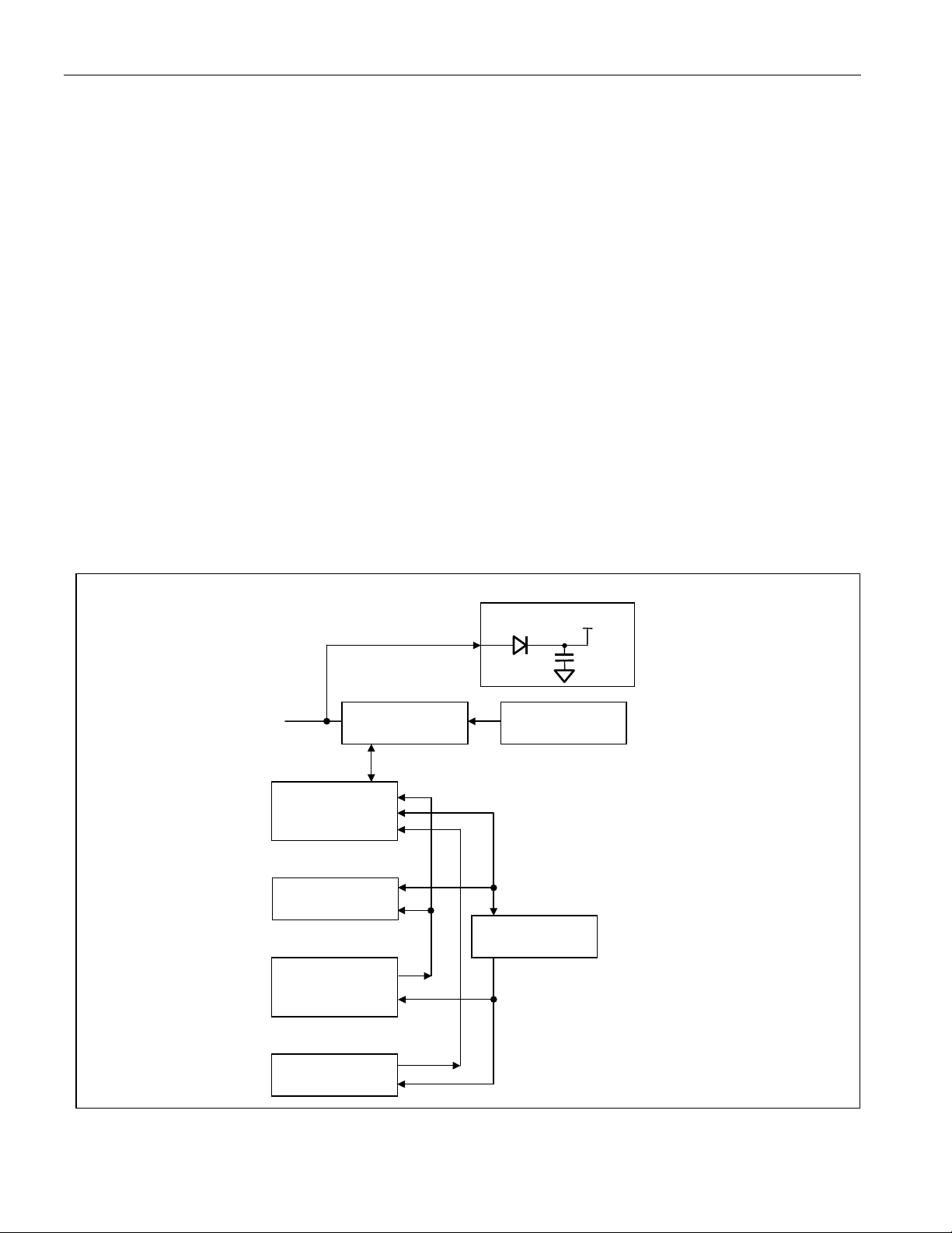
OVERVIEW
The block diagram in Figure 1 shows the relationships between the major control and memory sections of the
DS2431. The DS2431 has four main data components: 1) 64-bit lasered ROM, 2) 64-bit scratchpad, 3) four 32-byte
pages of EEPROM, and 4) 6 4- bit r egis t er pa ge. The hierarchical str uc ture of the 1-Wire protocol is shown i n Fig ur e
2. The bus master must first provide one of the seven ROM Function Commands, 1) Read ROM, 2) Match ROM, 3)
Search ROM, 4) Skip ROM, 5) Resum e, 6) Overdrive- Skip ROM or 7) Overdrive-Matc h ROM. Upon c ompletion of
an Overdrive ROM command byte executed at standard speed, the device enters Overdrive mode where all
subsequent comm unication occurs at a higher sp eed. The protoc ol requir ed for thes e ROM function c ommands is
described in Figure 9. After a ROM function command is successfully executed, the memory functions becom e
accessible and the master m ay provide any one of the four m emory function commands. The protoc ol for these
memory function commands is described in Figure 7. All data is read and written least significant bit first.
Figure 1. Block Diagram
I/O
Function Control
Memory
Function
Control Unit
CRC16
Generator
Data Memory
4 Pages of
256 bits each
1-Wire
PARASITE POWER
64-bit
Lasered ROM
DS2431
64-bit
Scratchpad
Register Page
64 bits
4 of 23
Page 5
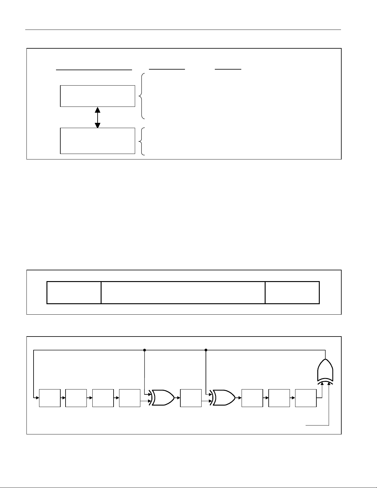
Figure 2. Hierarchical Structure for 1-Wire Protocol
DS2431: 1024-Bit, 1-Wire EEPRO M
DS2431 Co m m a nd Level:
1-Wire ROM Function
Commands (see Figure 9)
DS2431-specific
Memory Function
Commands (see Figure 7)
Available
Commands:
Read ROM
Match ROM
Search ROM
Skip ROM
Resume
Overdrive Skip
Overdrive Match
Write Scratchpad
Read Scratchpad
Copy Scratchpad
Read Memory
Data Field
Affected:
64-bit Reg. #, RC-Flag
64-bit Reg. #, RC-Flag
64-bit Reg. #, RC-Flag
RC-Flag
RC-Flag
64-bit Reg. #, RC-Flag, OD-Flag
64-bit Reg. #, RC-Flag, OD-Flag
64-bit Scratchpad, Flags
64-bit Scratchpad
Data Memory, Register Page
Data Memory, Register Page
64-BIT LASERED ROM
Each DS2431 contains a uniqu e ROM code that is 6 4 bits long. T he f irst 8 bits ar e a 1-W ire f amily code. T he next
48 bits are a unique serial number. The last 8 bits are a CRC (Cyclic Redundanc y Check) of the f irst 56 bits. See
Figure 3 for details. T he 1-Wire CRC is generated using a polynomial generator cons isting of a shift register and
XOR gates as shown in Figure 4. The polynomial is X
CRC is available in Application Note 27.
The shift register b its are initial ized to 0. Then s tarting with the least sig nificant bit of the f amily code, one bit at a
time is shifted in. Af ter the 8t h bit of the fam ily code has b een enter ed, then th e serial number is entered. After the
last bit of the serial number has been entered, the shift register contai ns the CRC value. Shifting i n the 8 bits of the
CRC returns the shift register to all 0s.
8
+ X5 + X4 + 1. Additional infor mation about the Dall as 1- Wire
Figure 3. 64-Bit Lasered ROM
MSB LSB
8-Bit
CRC Code
MSB LSB MSB LSB MSB LSB
Figure 4. 1-Wire CRC Generator
STAGE
0
X
st
1
STAGE
1
X
nd
2
2
X
rd
3
STAGE
STAGE
3
X
th
4
48-Bit Serial Number
Polynomial = X8 + X5 + X4 + 1
th
5
STAGE
4
X
STAGE
5
X
th
6
STAGE
6
X
INPUT DATA
8-Bit Family
Code (2Dh)
th
7
STAGE
7
X
8
th
8
X
5 of 23
Page 6

DS2431: 1024-Bit, 1-Wire EEPRO M
Figure 5. Memory Map
ADDRESS RANGE TYPE DESCRIPTION PROTECTION CODES
0000h to 001Fh R/(W) Data Memory Page 0
0020h to 003Fh R/(W) Data Memory Page 1
0040h to 005Fh R/(W) Data Memory Page 2
0060h to 007Fh R/(W) Data Memory Page 3
1)
0080h
0081h
0082h
0083h
0084h
1)
1)
1)
1)
R/(W) Protection Control Byte
Page 0
R/(W) Protection Control Byte
Page 1
R/(W) Protection Control Byte
Page 2
R/(W) Protection Control Byte
Page 3
55h: Write Protect P0; AAh: EPROM mode
P0; 55h or AAh: Write Protect 80h
55h: Write Protect P1; AAh: EPROM mode
P1; 55h or AAh: Write Protect 81h
55h: Write Protect P2; AAh: EPROM mode
P2; 55h or AAh: Write Protect 82h
55h: Write Protect P3; AAh: EPROM mode
P3; 55h or AAh: Write Protect 83h
R/(W) Copy Protecti on B yte 55h or AAh: Copy Protect 008 0:00 8Fh, and
any write-protected Pages
0085h R Factory byte. Set at
Factory.
AAh:Write Protect 85h, 86h, 87h;
55h: Write Protect 85h, unprotect 86h, 87h
0086h R/(W) User Byte/Manufacturer ID
0087h R/(W) User Byte/Manufacturer ID
0088h to 008Fh N/A Reserved
1)
Once programm ed to AAh or 5 5h this a ddress bec omes read-onl y. All oth er c odes can be s tored but will neith er
write-protect the address nor activate any function.
MEMORY
Data memory and regist ers are loc ated in a linear addres s spac e, as show n in Fi gure 5. T he data m emor y and t he
registers have unrestrict ed r e ad acc es s . T he DS 243 1 EE P RO M ar ra y co nsis ts of 18 rows of 8 bytes each. T he f irs t
16 rows are divided equally into 4 m emory pages (32 bytes each). These 4 pages ar e the primary data m emory.
Each page can be individually set to open (unprotected), write protected, or EPROM mode by setting the
associated protectio n byte in the regist er row. The last two r ows contain protect ion registers, an d reserved bytes .
The register row consists of 4 protection control bytes, a copy protection byte, the factory byte, and two user
byte/manufacture ID bytes. The m anufacturer ID can be a customer-suppl ied identification code that assists the
application software in identifying the product the DS2431 is associated with. Contact the f actory to set up and
register a custom manufacturer ID. The last row is reserved for future use. It is undefined in terms of R/W
functionality and should not be use d.
In addition to the main EEPROM array, an 8-byte vo latile s cratchpa d is inc luded. Writes to the EEPROM arr ay are
a two-step process. First, da ta is written to the scratchpa d, and then copied into the m ain array. This allows the
user to first verif y the data written to s cratchpad pr ior to c opying into the m ain arra y. The device on ly supports full
row (8-byte) copy operations. In order for data in the scratchpad to be valid for a copy operation, the address
supplied with a Write Scratchpad must start on a row boundary, and 8 full bytes must be written into the
scratchpad.
6 of 23
Page 7

DS2431: 1024-Bit, 1-Wire EEPRO M
The protection contr ol registers determine ho w incoming data on a write-scratchpad com mand is loaded into the
scratchpad. A protection setting of 55h (W rite Protect) causes the incoming data to be ingnored and t he target
address main memory data to be loaded into the scratchpad. A pr otection setting of AAh (EPROM Mode) c auses
the logical AND of incoming data and target address main memory data to be loaded into the scratchpad. Any
other protection control register setting leaves the associated m emory page open for unrestricted write access.
Protection control b yte settings of 55h or AAh also wr ite protect the protection control b yte. The prot ection-contro l
byte setting of 55h does n ot block the cop y. This allows write-protected data t o be refreshed ( i. e., reprogramm ed
with the current data) in the device.
The copy protection b yte is used for a higher level of security, and should only be used after all other protection
control bytes, user bytes, and writ e-protected pag es are set to their fin al value. If t he copy protec tion b yte is set to
55h or Aah, all copy attem pts to the register row and user byte row are block ed. In addition, all copy attem pts to
write-protected main memory pages (i. e., refresh) are blocked.
ADDRESS REGISTERS AND TRANSFER STATUS
The DS2431 employs three address register s: T A1, TA2, and E/S (Figure 6) . T hes e r egist er s are c om mon to man y
other 1-Wire devices but operate slig htly differ ently with the D S2431. Register s TA1 and T A2 must be lo aded with
the target address to which the data is written or from which data is re ad. Register E/S is a read-only tr ansferstatus register, used to verify data integrity with write commands. ES bits E2:E0 are loaded with the incoming
T2:T0 on a write-scratchpad command, and increment on each subsequent data byte. This is in effect a byteending offset counter within the 8-b yte scratchpad. Bit 5 of the E/S register, cal led PF, is a logic 1 if the data in the
scratchpad is not va li d du e to a los s of po wer or if the master sends l es s b ytes tha n n eed ed to reach the end of the
scratchpad. For a valid wr ite to the s cratchpa d, T2:T 0 must be 0 and t he m aster mus t have sent 8 da ta bytes . Bits
3, 4, and 6 have no function; they always read 0. The highest valued bit of the E/S register, called AA or
Authorization Accepted, ac ts as a flag to indicat e that the data stor ed i n the sc ratchpa d has alre ad y been copi ed to
the target memory address. Writing data to the scratchpad clears this flag.
Figure 6. Address Registers
Bit #76543210
Target Address (TA1)T7T6T5T4T3T2T1T0
Target Address (TA2) T15 T14 T13 T12 T11 T10 T9 T8
Ending Address with
Data Status (E/S)
(Read Only)
AA 0 PF 0 0E2E1E0
7 of 23
Page 8

DS2431: 1024-Bit, 1-Wire EEPRO M
WRITING WITH VERIFICATION
To write data to the DS2431 , the scratchpad has to b e used as intermediat e storage. First the master issues the
Write Scratchpad command to specify the desired target address, followed by the data to be written to the
scratchpad. Note that Copy Scratchpad com mands must be perf ormed on 8-byte bo undaries, i. e., the 3 L SBs of
the target address (T2..T0) mus t be equal to 000b. If T 2..T 0 ar e sent with no n- zero v alu es, the copy function wil l be
blocked. Under certai n conditions (see Write Scr atchpad comm and) the master will receive an inverte d CRC16 of
the command, address (actual addres s sent) and data at the end of the Write Scr atchpad command sequence.
Knowing this CRC value, the master can compare it to the value it has calculated itself to decide if the
communication was s ucces sf ul and proc eed to the Copy Scra tchpa d com m and. If the m as ter could no t r eceive the
CRC16, it should send t he Read Scratchpad comm and to verify data integrit y. As a preamble t o the scratchpad
data, the DS2431 repeats the target addres s TA1 and TA2 and sends th e contents of the E/S regis ter. If the PF
flag is set, data did n ot arr i ve c orr ectly in the scratchpad or th er e was a loss of po wer s ince dat a was last wr itten to
the scratchpad. The master does not need to continue reading; it can start a new trial to write data to the
scratchpad. Similarl y, a set AA flag to gether with a c leared PF flag in dicates that the device did n ot recognize the
Write command. If everything went correctly, both flags are cleared. Now the master can continue reading and
verifying every dat a byte. After the master has verified the data, it can sen d the Copy Scratc hpad command, f or
example. This comm and must be followed exactl y by the data of the three address registers, TA1, TA2, and E/S.
The master should obtain the contents of these registers by reading the scratchpad.
MEMORY FUNCTION COMMANDS
The Memory Funct ion Flow Chart (Figure 7) describes th e protocols necessary for ac cessing the memory of the
DS2431. An example on how to use these func tions to write to a nd read from the device is incl uded at the end of
this document. The communic ation bet wee n m as ter and DS2431 t akes place either at regul ar s pee d (def au lt, O D =
0) or at Overdrive Speed (OD = 1). If not explicitly set into the Overdrive Mode, the DS2431 assumes regular
speed.
WRITE SCRATCHPAD COMMAND [0Fh]
The Write Scratchpad comm and applies to the data mem ory, and the writable addresses i n the register page. In
order for the scratchpad data to be valid for copying to the array, the user must perform a Write Scratchpad
command of 8 bytes starting at a valid row bou ndary. The W rite Scratchpad com mand accepts in valid addres ses,
and partial rows, but subsequent Copy Scratchpad commands are blocked.
After issuing the Write Scratchp ad command, the master must first provide th e 2-byte target a ddress, followed b y
the data to be written to the scratchpad. T he data is written to th e scratchpad startin g at the byte off set of T2:T0.
The ES bits E2:E0 ar e loaded with the starting b yte offset, and increment with eac h susequent byte. Effec tively,
E2:E0 is the byte offset of the last full byte written to the scratchpad. Only full data bytes are accepted.
When executing the Write Sc ratchpad command, the CRC gener ator inside the DS2431 (Figure 13) c alculates a
CRC of the entire data stream, starting at the command code and ending at the last data byte as sent by the
master. This CRC is generat ed using the CRC16 p olynomial b y first clearing the CRC generat or and then shif ting
in the command code ( 0FH) of the W rite Scratchpad com mand, the Tar get Addresses ( TA1 and TA2), and all the
data bytes. Note that the CRC16 calculation is performed with the actual TA1 and TA2 and data sent by the
master. The master may end the W rite Scratc hpad com mand at an y time. Howev er, if th e end of the scratchpad is
reached (E2:E0 = 111b), the master may send 16 read-time slots and receive the CRC generated by the DS2431.
If a Write Scratchpad is attempted to a write- protected location, the sc ratchpad is loaded with the data already in
memory, rather than the data transm itted. Similarl y, if the target ad dress page is in EPRO M mode, the sc ratchpad
is loaded with the bitwise logical AND of the transmitted data and data already in memory.
8 of 23
Page 9

Figure 7-1. Memory Function Flow Chart
(
)
(Fig
)
(Fig
)
p
DS2431: 1024-Bit, 1-Wire EEPRO M
DS2431
Increments
E2:E0
Bus Master TX Memory
Function Command
0Fh
Write Scratch-
pad ?
Y
Bus Master TX
T7:T0), TA2 (T15:T8
TA1
DS2431 sets
Sets PF = 1
Clears AA = 0
Sets E2:E0 = T2:T0
Master TX Data Byte
To Scratch
ad
Master
TX Reset ?
N
E2:E0
N
= 7 ?
Y
T2:T0
= 0 ?
Y
From ROM Functions
Flow Chart
N
ure 9
To Figure 7
nd
Part
2
Applies only if the
memory area is not
protected.
Y
If
write-protected
, then
the DS2431 copies the
data byte from the target address into the SP.
If in
EPROM mode
,
then the DS2431 loads
the bitwise logical AND
of the transmitted byte
and the data byte from
N
the targeted address
into the SP.
Bus Master
RX “1”s
PF = 0
DS2431 TX CRC16
of Command, Address,
Data Bytes as th e y we r e
sent by the bus master
N
Master
TX Reset ?
Y
To ROM Functions
Flow Chart
9 of 23
ure 9
From Figure 7
nd
Part
2
Page 10

Figure 7-2. Memory Function Flow Chart (continued)
y
y
y
y
y
DS2431: 1024-Bit, 1-Wire EEPRO M
From Figure 7
st
Part
1
DS2431
Increments
B
te Counter
AAh
Read Scratch-
Pad ?
Y
Bus Master RX
TA1 (T7:T0), TA2 (T15:T8)
and E/S B
te
DS2431 sets Scratchpad
B
te Counter = T2:T0
Bus Master RX
Data B
te from Scratchpad
Master
Y
TX Reset ?
N
N
Byte Counter
= E2:E0 ?
To Figure 7
N
rd
Part
3
To Figure 7
st
1
Part
Bus Master
RX “1”s
Y
Bus Master RX CRC16
of Command, Address,
E/S Byte, Data Bytes as
the DS2431
sent b
N
Master
TX Reset ?
Y
From Figure 7
rd
3
Part
10 of 23
Page 11

Figure 7-3. Memory Function Flow Chart (continued)
y
p
DS2431: 1024-Bit, 1-Wire EEPRO M
From Figure 7
nd
Part
2
TA1 (T7:T0), TA2 (T15:T8)
55h
Copy Scratch-
Pad ?
Y
Bus Master TX
and E/S B
te
Auth. Code
Match ?
N
To Figure 7
N
4
th
Part
Applicable to all R/W
memory locations.
Y
T15:T0
Y
< 0090h ?
N
N
PF = 0 ?
Y
Y
Copy-
Protected ?
N
AA = 1
To Figure 7
nd
2
Part
Bus Master
RX “1”s
Master
TX Reset ?
Y
* 1-Wire idle high for power
DS2431 copies Scratch-
*
ad Data to Address
DS2431 TX “0”
Y
Master
TX Reset ?
N
N
DS2431 TX “1”
Master
N
TX Reset ?
Y
From Figure 7
th
4
Part
11 of 23
Page 12
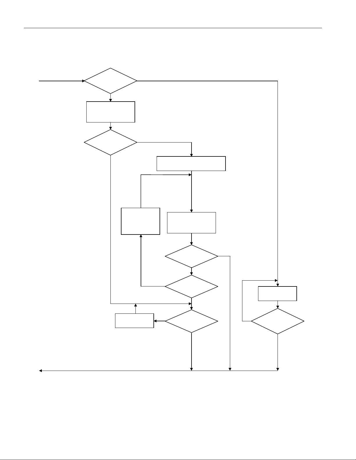
Figure 7-4. Memory Function Flow Chart (continued)
(
)
(
)
y
From Figure 7
3
rd
Part
F0h
Read Memory ?
Y
Bus Master TX
TA1 (T7:T0),
TA2
T15:T8
N
DS2431: 1024-Bit, 1-Wire EEPRO M
Address
< 90h ?
N
DS2431
Increments
Address
Y
Counter
DS2431 sets Memory
Address =
T15:T0
Bus Master RX
Data Byte from
Memor
Address
Master
TX Reset ?
N
Y
Address
< 8Fh ?
N
Y
Bus Master
RX “1”s
N
Master
TX Reset ?
Y
To Figure 7
rd
3
Part
Bus Master
RX “1”s
N
Master
TX Reset ?
Y
12 of 23
Page 13

DS2431: 1024-Bit, 1-Wire EEPRO M
READ SCRATCHPAD COMMAND [AAh]
The Read Scratchpad c ommand allo ws verifying the t arget address and t he integrity of the scratchpa d data. After
issuing the command code, the m aster begins reading. The f irst two b ytes are the tar get addres s. The nex t byte is
the ending offset/data status byte (E/S) followed by the scratchpad data, which may be different from what the
master originally sent. This is of particular importanc e if the target address is within the regis ter page or a pag e in
either Write Protection or EPROM modes. See the Write Scratchpad description for details. The master should
read through the scratc hpad (E2: E0 – T 2:T 0 + 1 bytes) , after which it will rece ive t he in verted CRC, bas ed on data
as it was sent by the DS2431. If the master continues reading after the CRC, all data will be logic 1s.
COPY SCRATCHPAD [55h]
The Copy Scratchpad command is used to copy data from the scratchpad to writable memory sections. After
issuing the Copy Sc ratc hp ad c om mand, the master must provide a 3-byte authorization patter n , which should have
been obtained by an immediatel y preceding Read Scratchpad comm and. This 3-byte pattern must ex actly match
the data contained in the three address reg isters (TA1, TA2, E/S, in that order). If the pattern matches, the tar get
address is valid, the PF flag is not set, and the target memory is not copy-protected, the AA (Authorization
Accepted) flag is set and the cop y begins. All eight b ytes of scratchpad co ntents are copie d to the target m emory
location. The devic e ’s in ter na l d ata trans f er takes 13ms maximum during which the volt ag e on the 1- Wire bus m ust
not fall below 2.8V. A pattern of alternating 0s and 1s are transmitted after the data has been copied until the
master issues a reset pulse. If the PF f lag is s et or t he ta r get memory is copy-protec ted, t he c opy will not begin and
the AA flag will not be set.
READ MEMORY [F0h]
The Read Memory command is th e ge ner a l f unction to read data from the DS2431. After is suin g th e c om mand, the
master must provide the 2-byte targ et address. After these two b ytes, the master reads data beg inning from the
target address and may continue unti l address 008Fh. If the master continues reading, the res ult will be logic 1s.
The device's internal TA1, TA2, E/S, and scratchpad contents are not affected by a Read Memory command.
1-Wire BUS SYSTEM
The 1-Wire bus is a system that has a s ingle b us mas ter and one or m ore s laves. In all instances the DS24 31 is a
slave device. The bus m aster is t ypically a micr ocontroller. The d iscussion of this bus system is broken down into
three topics: hardware configuration, transaction sequence, and 1-Wire signaling (signal types and timing). The
1-Wire protocol def ines bus transact ions in term s of the bus state d uring specific time slots, whic h are initiat ed on
the falling edge of sync pulses from the bus master.
HARDWARE CONFIGURATION
The 1-Wire bus has only a sin gle line b y definit ion; it is important that each device on the bus be able to dr ive i t at
the appropriate time. To facilitat e this, each device attached to the 1-W ire bus must have open-drain or tr i-state
outputs. The 1-Wire port of the DS2431 is open drain with an internal circuit equivalent to that shown in Figure 8.
A multidrop bus co nsists of a 1- Wire bus with multiple sl aves att ached . T he DS2431 sup ports bot h a St andar d a nd
Overdrive communication speed of 15.4kbps (max) and 111kbps (max), respectively. Note that legacy 1-Wire
products support a st andard communication speed of 16. 3kbps and Overdrive of 142kbps. T he slightly reduced
rates for the DS2431 are a result of additional recovery times, which in turn were driven by a 1-Wire physical
interface enhancement to improve noise immunity. The value of the pullup resistor primarily depends on the
network size and load conditions. The DS2431 requires a pullup resistor of 2.2kΩ (max) at any speed.
The idle state for th e 1-W ire bus is hi gh. If for any reason a transac tion needs t o be sus pended, th e bus MUST be
left in the idle sta te if the tr ansac tion is to resum e. If this does not occur and the bus is lef t low for more than 16µs
(Overdrive speed) or more than 120µs (standard speed), one or more devices on the bus may be reset.
13 of 23
Page 14

Figure 8. Hardware Configuration
BUS MASTER DS2431 1-Wire PORT
DS2431: 1024-Bit, 1-Wire EEPRO M
V
PUP
R
PUP
RX
TX
Open Drain
Port Pin
RX = RECEIVE
TX = TRANSMIT
2.2µA
Max.
100
MOSFET
RXDATA
TX
Ω
TRANSACTION SEQUENCE
The protocol for accessing the DS2431 through the 1-Wire port is as follows:
! Initialization
! ROM Function Command
! Memory Function Command
! Transaction/Data
INITIALIZATION
All transactions on the 1-W ire bus begin with an initialization sequ ence. The initialization s equence consists of a
reset pulse transmitted by the bus mas ter followed b y presence pulse( s) transm itted b y the slave(s ). The pres ence
pulse lets the bus master know that the DS2431 is on the bus and is ready to operate. For more details, see the
1-Wire Signaling section.
1-Wire ROM FUNCTION COMMANDS
Once the bus mas ter has detected a presence, it can issue one of the seven ROM f unction commands that th e
DS2431 supports. Al l ROM functio n comm ands are 8 bits lon g. A list of these com mands follo ws (refer to the flow
chart in Figure 9).
READ ROM [33h]
This command allows the bus m aster to read the DS2431’s 8-bit famil y code, u ni que 48- bit s eri al number, and 8-bit
CRC. This command can only be used if there is a single slave on the bus. If more than one slave is present on the
bus, a data collision occurs when all slaves try to transm it at the same time (open drain produces a wired-AND
result). The resultant family code and 48-bit serial number result in a mismatch of the CRC.
MATCH ROM [55h]
The Match ROM command, followed by a 64-bit ROM sequence, allows the bus master to address a specific
DS2431 on a multidrop bus. Only the DS2431 that exactly matches the 64-bit ROM sequence responds to the
following mem ory function command. All other sla ves wait for a reset pulse. This command can be used with a
single or multiple devices on the bus.
14 of 23
Page 15

DS2431: 1024-Bit, 1-Wire EEPRO M
SEARCH ROM [F0h]
When a system is initiall y brought up, the b us mas ter might not k now the n umber of devices on th e 1-W ire bus or
their registration numbers. By taking advantage of the wired-AND property of the bus, the master can use a
process of elimination to identify the registration numbers of all slave devices. For each bit of the registration
number, starting with the l east significant bit, the bus m aster issues a triplet of tim e slots. On the first slot, each
slave device participating in the search outputs the true val ue of its registration number bit. On the second slot,
each slave device par tic ipating in the s earc h outputs the c om plem ented val ue of its r egistrat ion num ber bit. On t he
third slot, the master writes the true value of the bit to be selected. All slave devices that do not m atch the bit
written by the master s top participat ing in th e search. If b oth of the read bits ar e zero, th e mas ter knows that s lave
devices exist with both states of the bit. By choos ing whic h state to wr ite, the bus mas ter branches in the rom code
tree. After one com plete pass, th e bus m aster k nows the regis tration num ber of a single d evice. Addition al pass es
identify the registr ation num bers of the rem aining dev ices. Refer to Appl ication N ote 187: 1-Wir e Search Algor ithm
for a detailed discussion, including an example.
SKIP ROM [CCh]
This command can save time in a single-drop bus system by allowing the bus master to access the memory
functions without providing the 64- bit ROM code. If more than one s lave is presen t on the bus and, for exam ple, a
Read command is issued follo wing the Skip ROM command, data collis ion occurs on the bus as m ultiple slaves
transmit simultaneously (open-drain pulldowns produce a wired-AND result).
RESUME [A5h]
To maximize the data throughput in a multidrop environment, the Resume function is available. This function
checks the status of the RC bit and, if it is set, directly transfers control to the Memory functions, similar to a Skip
ROM command. The only way to set the RC bit is t hr oug h suc c ess f ull y exec uting th e Matc h ROM, Search ROM, or
Overdrive Match ROM command. Once the RC bit is set, the device can repeatedly be accessed through the
Resume Command function. Accessing another device on the bus clears the RC bit, preventing two or more
devices from simultaneously responding to the Resume Command function.
OVERDRIVE SKIP ROM [3Ch]
On a single-drop bus this comm and can save time b y allowing the bus master to access the memor y functions
without providing the 64-bit ROM c ode. Unlike the nor mal Skip ROM c ommand, the O verdrive Sk ip ROM sets the
DS2431 in the Overdr ive mode (OD = 1). All comm unication following this c ommand has to occur at Overdrive
speed until a reset pulse of minimum 480µs duration resets all devices on the bus to standard speed (OD = 0).
When issued on a multidrop bus, this command sets all Overdrive-supporting devices into Overdrive mode. To
subsequently address a specific Overdrive- supporting device, a res et pulse at Overdrive speed has to be issued
followed by a Match ROM or Search ROM comm and sequence. T his spee ds up the tim e f or the search pr ocess. If
more than one slave supporting Overdr i ve is present on the bus and the O verdri ve Skip ROM command is f oll owe d
by a Read command, data collision occurs on the bus as multiple slaves transmit simultaneously (open-drain
pulldowns produce a wired-AND result).
OVERDRIVE MATCH ROM [69h]
The Overdrive Match RO M command follo wed by a 64-bit ROM sequ ence transmitted at O verdrive Speed a llows
the bus master to address a specific DS2 431 on a multidrop b us and to simultaneous ly set it in Overdrive mode.
Only the DS2431 that exac tly matches the 64-bit ROM sequence res ponds to the subsequent m emory function
command. Slaves already in Overdrive mode from a previous Overdrive Skip or successful Overdrive Match
command remain in Overdrive mode. All overdrive-capable slaves return to standard speed at the next Reset Pulse
of minimum 480µs duration. The Overdri ve Match ROM com m and can be used with a sing le or m ulti ple dev ices on
the bus.
15 of 23
Page 16

Figure 9-1. ROM Functions Flow Chart
)
y
(Fig
)
Bus Master TX
From Memory Functions
Flow Chart
ure 7
Reset Pulse ?
Reset Pulse
OD
Y
DS2431: 1024-Bit, 1-Wire EEPRO M
From Figure 9, 2nd Part
N
OD = 0
Bus Master TX ROM
Function Command
33h
Read ROM
Command ?
RC = 0
DS2431 TX
Family Code
(1 Byte)
DS2431 TX
Serial Number
(6 Bytes)
DS2431 TX
Presence Pulse
N
55h
Match ROM
Command ?
RC = 0
Master TX Bit 0
Bit 0
Match ?
Master TX Bit 1
Bit 1
Match ?
N
N
N
Y
N
N
Y
F0h
Search ROM
Command ?
YY YY
RC = 0
DS2431 TX Bit 0
DS2431 TX Bit 0
Master TX Bit 0
Bit 0
Match ?
Y
DS2431 TX Bit 1
DS2431 TX Bit 1
Master TX Bit 1
Bit 1
Match ?
Y
N
CCh
Skip ROM
Command ?
RC = 0
To Figure 9
2nd Part
N
DS2431 TX
CRC B
te
Master TX Bit 63
Bit 63
Match ?
Y
RC = 1
N
To Memory Functions
Flow Chart (Figure 7
DS2431 TX Bit 63
DS2431 TX Bit 63
Master TX Bit 63
N
Bit 63
Match ?
RC = 1
Y
To Figure 9
2nd Part
From Figure 9
nd
Part
2
16 of 23
Page 17
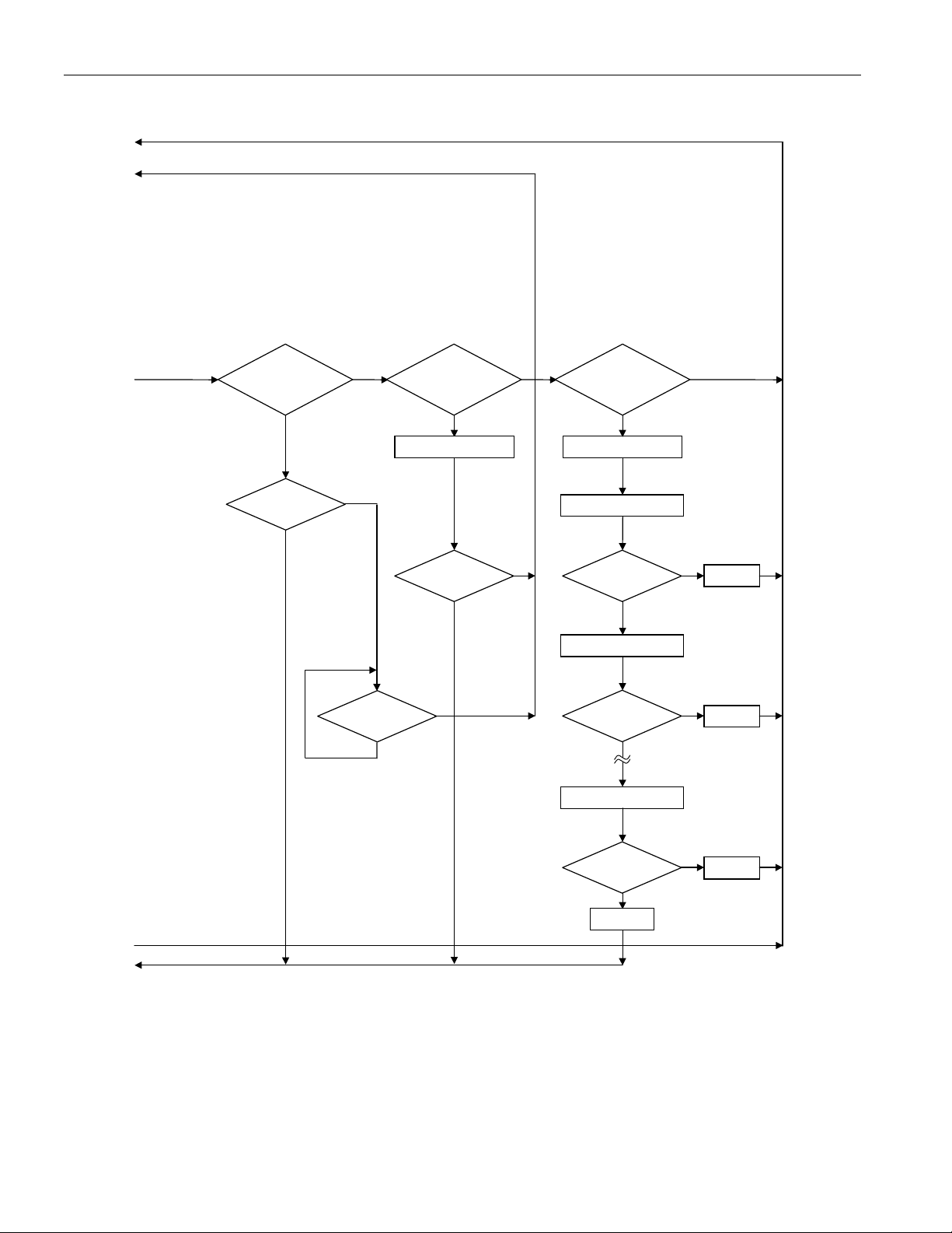
Figure 9-2. ROM Functions Flow Chart (continued)
To Figure 9, 1st Part
From Figure 9
1
st
Part
A5h
Resume
Command ?
N
3Ch
Overdrive
Skip ROM ?
DS2431: 1024-Bit, 1-Wire EEPRO M
N
69h
Overdrive Match
ROM ?
N
From Figure 9
st
1
Part
RC = 1 ?
Y
Y
N
Master
TX Reset ?
N
Y
RC = 0 ; OD = 1
Master
TX Reset ?
N
Y
Y
RC = 0 ; OD = 1
Master TX Bit 0
Y
Bit 0
Match ?
N
OD = 0
Y
Master TX Bit 1
Bit 1
Match ?
N
OD = 0
Y
Master TX Bit 63
Bit 63
Match ?
N
OD = 0
Y
RC = 1
To Figure 9
st
1
Part
17 of 23
Page 18

DS2431: 1024-Bit, 1-Wire EEPRO M
1-Wire SIGNALING
The DS2431 requires strict pr otocols to ensure data integr ity. The protocol consists of four types of signaling on
one line: Reset Sequence with Reset Puls e and Presence Pulse, Wr ite-Zero, Write-One, and Read-Dat a. Except
for the Presence pu lse, the bus master initiates all falling edges. The D S2431 can communicate at t wo different
speeds, standard speed, and Overdrive Speed. If not explicitly set into the Overdrive mode, the DS2431
communicates at standard speed. While in Overdrive Mode the fast timing applies to all waveforms.
To get from idle to ac tive, the voltage on the 1- Wire line needs to fall from V
from active to id le, the vo ltage nee ds to rise from V
past the threshold VTH. The time it takes for the voltage to
ILMAX
make this rise is seen in Figure 10 as 'ε' and its duration depends on the pullup resistor (R
capacitance of the 1-W ire network attached.
The voltage V
is relevant for the DS2431 when determining a
ILMAX
below the threshold VTL. To get
PUP
) used and the
PUP
logical level, not triggering any events.
Figure 10 shows the init ialization sequence re quired to be gin any comm unication with the DS243 1. A Reset Pul se
followed by a Prese nce Pulse in dicates the DS 2431 is read y to receive data, g iven the correct RO M and mem ory
function comm and. If the bus master uses slew-r ate c ontro l o n th e falling edge, it must pull do wn t he line for t
t
to compensate for the edg e. A t
F
standard speed. If the DS2431 is in Overdrive Mode and t
duration of 480µs or longer exits t he Overdr iv e Mode, re turn ing the devic e to
RSTL
is no longer than 80µs. the device remains in
RSTL
RSTL
+
Overdrive Mode.
Figure 10. Initialization Procedure: Reset and Presence Pulse
MASTER TX “RESET PULSE” MASTER RX “PRESENCE PULSE”
t
t
PDH
MSP
t
PDL
t
RSTH
t
REC
V
IHMASTER
V
V
PUP
V
TH
V
ILMAX
0V
ε
TL
t
F
t
RSTL
RESISTOR MASTER DS2431
After the bus master has release d the line it goes in to rece ive m ode. Now the 1- W ire bus is pulled to V
the pullup resistor, or in case of a DS2482-x 00 or DS2480B driver, b y active circuitry. W hen the thresho ld V
crossed, the DS2431 wa its f or t
presence pulse, the master must test the logical state of the 1-Wire line at t
The t
window must be at leas t the sum of t
RSTH
DS2431 is ready for da ta communication. In a mixed population network, t
and then transm its a Pr esence Puls e b y pullin g the l ine lo w for t
PDH
PDHMAX
, t
PDLMAX
, and t
RECMIN
.
MSP
. Immediately after t
should be extended to m inimum
RSTH
PDL
is expired, the
RSTH
through
PUP
TH
is
. To detect a
480µs at standard speed and 48µs at Overdrive speed to accommodate other 1-Wire devices.
Read-/Write-Time Slots
Data communication with the DS2431 takes place in time slots, which carry a single bit each. Write-time slots
transport data from bus master to s lave. Read-time slots transf er data from slave to master. F igure 11 illustrates
the definitions of the write- and read-time slots.
All communication begins with the m aster pulling the data line lo w. As the voltage on t he 1- Wire line falls below the
threshold V
a write-time slot and how long data is valid during a read-time slot.
, the DS2431 starts its intern al tim ing generat or that deter mines whe n the da ta line is s ampled during
TL
18 of 23
Page 19

DS2431: 1024-Bit, 1-Wire EEPRO M
Master-to-Slave
For a write-one time slot, the voltage on the data line must have crossed the VTH threshold befor e the write-one
low time t
threshold until the write-zero low time t
data line should not ex ceed V
the DS2431 needs a recovery time t
Figure 11. Read/Write Timing Diagram
Write-One Time Slot
is expired. For a write-zero time slot, the voltage on the data line must stay below the V
W1LMAX
is expired. For the m ost reliable comm unication, the voltage on the
V
IHMASTER
V
V
PUP
V
TH
V
ILMAX
W0LMIN
during the entire t
ILMAX
t
W1L
TL
before it is ready for the next time slot.
REC
W0L
or t
window. After the VTH threshold has been c rossed,
W1L
0V
t
F
ε
t
SLOT
RESISTOR MASTER
TH
Write-Zero Time Slot
V
PUP
V
IHMASTER
V
TH
V
TL
V
ILMAX
0V
t
F
Read-Data Time Slot
V
PUP
V
IHMASTER
V
TH
V
TL
V
ILMAX
0V
t
F
t
W0L
t
SLOT
RESISTOR MASTER
t
t
RL
MSR
Master
Sampling
Window
δ
t
SLOT
t
REC
t
REC
RESISTOR MASTER DS2431
19 of 23
Page 20

DS2431: 1024-Bit, 1-Wire EEPRO M
Slave-to-Master
A read-data time slot begins lik e a write- on e t ime slot. The voltage o n th e d ata li ne must remain below VTL until the
read low time t
line low; its internal timing generat or deter m ines when this pulld own ends and the vo ltage st arts r ising ag ain. W hen
responding with a 1, the DS2431 does not hold the data line low at all, and the voltage starts rising as soon as t
over.
is expired. During th e tRL window, when resp onding with a 0, the D S2431 starts pull ing the data
RL
RL
is
The sum of t
the master sampling window (t
most reliable c ommunication, t
later than t
sufficient recovery time t
applies only to a single DS2431 attached to a 1-Wire line. For multidevice configurations, t
+ δ (rise time) on one side and the in ternal t iming gener ator of the DS2431 on the oth er side def ine
RL
. After reading from the data line, the m aster must wait until t
MSRMAX
for the DS2431 to get ready for the next time slot. Note that t
REC
to t
MSRMIN
should be as short as permissible, and the m aster should read clos e to but no
RL
) in which the master must perf orm a r ead f r om the data l ine. F or the
MSRMAX
is expired. This guarantees
SLOT
specified herein
REC
REC
needs to be
extended to accommodate the addit ional 1-W ire device input c apacitance. A lternatively, a n interf ace that perf orms
active pullup during the 1-Wire recovery time such as the DS2482-x00 or DS2480B 1-W ire line drivers can be
used.
IMPROVED NETWORK BEHAVIOR (SWITCHPOINT HYSTERESIS)
In a 1-Wire environment, line term ination is possible only during transients contro lled by the bus master (1-W ire
driver). 1-W ire networks , therefore, ar e suscept ible to no ise of various or igins. De pending o n the p hysical si ze and
topology of the net work, reflections fr om end points and bra nch points can add up, or cancel each other to some
extent. Such reflec tions ar e vis ible as glitc hes or ringi ng on t he 1-Wire communication li ne. Noise c oupled on to t he
1-Wire line from external sourc es can als o res ult in s igna l gl itchi ng. A g li tc h d uring th e r isin g e dge of a time slot can
cause a slave device to lose synchroni zation with the m as ter and, co nsequ entl y, result i n a se arch ROM c omm and
coming to a dead end or cause a device-specific f unction command to abort. For be tter performance in network
applications, the DS2431 uses a new 1-Wire front end, which m akes it les s sens itive to no ise an d also r educ es th e
magnitude of noise injected by the slave device itself.
The 1-Wire front end of the DS2431 differs from traditional slave devices in four characteristics.
1) The falling edge of the presence pulse has a controlled slew rate. This provides a better match to the line
impedance than a digitally switched transistor, converting the high-frequency ringing known from traditional
devices into a smoother low-bandwidth transition. The slew-rate control is specified by the parameter t
which has different values for standard and Overdrive speed.
2) There is additional low-pas s filtering in the cir cuit that detects the f alling edge at the begi nning of a time slot.
This reduces the sensitivity to high-frequency noise. This additional filtering does not apply at Overdrive speed.
3) There is a hysteresis at the low-to-high switching threshold V
below V
- VHY, it will not be recognized (Figure 12, Case A). The hysteresis is effective at any 1-Wire speed.
TH
4) T here is a tim e windo w spec ified by th e risin g edge hold- off tim e t
they extend below V
appear late after cr ossing the V
- VHY threshold (Figure 12, Cas e B, tGL < t
TH
threshold and extend be yond the t
TH
taken as the beginning of a new time slot (Figure 12, Case C, t
Only devices that have the parameters t
, VHY, and t
FPD
REH
. If a negative g litc h cr os s es VTH but does not go
TH
during which glit ches ar e ign ored, even if
REH
). Deep voltage dr oops or glitches that
REH
window cannot be filtered out and are
REH
≥ t
REH
).
GL
specified in their electrical characteristics use the
improved 1-Wire front end.
FPD
,
Figure 12. Noise Suppression Scheme
V
PUP
V
TH
V
HY
Case A Case CCase B
0V
t
REH
t
GL
20 of 23
t
REH
t
GL
Page 21

DS2431: 1024-Bit, 1-Wire EEPRO M
CRC GENERATION
With the DS2431 there are two different types of CRCs. One CRC is an 8-bit type and is stored in the most
significant byte of the 64-bit ROM. The bus master can compute a CRC value f rom the first 56 bits of the 64-bit
ROM and compare it t o the val ue store d with in t he DS24 31 to d eterm ine if the ROM data has b een recei ved er rorfree. The equivalen t polynomial function of this CRC is X
(noninverted) form. It is computed at the factory and lasered into the ROM.
8
+ X5 + X4 + 1. This 8-bit CRC is received i n the true
16
The other CRC is a 16-b it type, g enerated accordin g to the s tandardize d CRC 16-polynom ial f unction x
+ x15 + x
+ 1. This CRC is use d for fast verification of a data tra nsfer when writing to or reading f rom the scratchpad. In
contrast to the 8-bit CRC, the 16-bit CRC is always communicated in the inverted form . A CRC gen erator inside the
DS2431 chip (Figure 13) calcul ates a new 16-bit CRC, as shown in the command flow c hart (Figure 7). The bus
master compares the CRC value read f rom the dev ice to the one it calculat es from the data, an d decides whether
to continue with an operation or to reread the portion of the data with the CRC error.
With the Write Scratchpad command, the CRC is generate d by first clearing the CRC gen erator and the n s hif tin g in
the command code, the Target Addresses TA1 and TA2, and all the data bytes as they were sent by the bus
master. The DS2431 transmits this CRC only if E2:E0 = 111b.
With the Read Scratchpad command, the CRC is gen erate d by first clearing the CRC gener ator a nd t hen shif tin g i n
the Command code, the Tar get Addres ses T A1 and T A2, th e E/S byte, and the s cratchp ad data as the y were se nt
by the DS2431. The DS 2431 transmits this CRC on ly if the reading cont inues through the end of the scratchpad.
For more information on generating CRC values, refer to
Application Note 27
.
Figure 13. CRC-16 Hardware Description and Polynomial
Polynomial = X16 + X15 + X2 + 1
st
1
STAGE
nd
2
STAGE
rd
3
STAGE
th
4
STAGE
th
5
STAGE
th
6
STAGE
th
7
STAGE
th
8
STAGE
2
0
X
8
X
9
STAGE
1
X
th
STAGE
9
X
10
th
11
th
STAGE
10
X
STAGE
11
X
2
X
th
12
STAGE
12
X
3
X
th
13
13
X
4
X
th
14
STAGE
14
X
5
X
th
15
STAGE
6
X
7
X
th
16
STAGE
15
X
16
X
CRC
OUTPUT
INPUT DATA
COMMAND-SPECIFIC 1-Wire COMMUNICATION PROTOCOL—COLOR CODES
Master to slave Slave to master Programming
21 of 23
Page 22

DS2431: 1024-Bit, 1-Wire EEPRO M
COMMAND-SPECIFIC 1-Wire COMMUNICATION PROTOCOL—LEGEND
SYMBOL DESCRIPTION
RST 1-Wire Reset Pulse generated by master.
PD 1-Wire Presence Pulse generated by slave.
Select Command and data to satisfy the ROM function protocol.
WS Command "Write Scratchpad".
RS Command "Read Scratchpad".
CPS Command "Copy Scratchpad".
RM Command "Read Memory".
TA Target Address TA1, TA2.
TA-E/S Target Address TA1, TA2 with E/S byte.
<8 – T2:T0 bytes>
<data to EOM> Transfer of as many data bytes as are needed to reach the end of the memory.
CRC16\ Transfer of an inverted CRC16.
FF loop Indefinite loop where the master reads FF bytes.
AA loop Indefinite loop where the master reads AA bytes.
Programming Data transfer to EEPROM; no activity on the 1-Wire bus permitted during this time.
Transfer of as many bytes as needed to reach the end of the scratchpad for a given
target address.
WRITE SCRATCHPAD (CANNOT FAIL)
RST PD Select WS TA <8 – T2:T0 bytes> CRC16\ FF loop
READ SCRATCHPAD (CANNOT FAIL)
RST PD Select RS TA-E/S <8 – T2:T0 bytes> CRC16\ FF loop
COPY SCRATCHPAD (SUCCESS)
RST PD Select CPS TA-E/S Programming AA lo op
COPY SCRATCHPAD (INVALID ADDRESS OR PF = 1 OR COPY PROTECTED)
RST PD Select CPS TA-E/S FF loop
READ MEMORY (SUCCESS)
RST PD Select RM TA <data to EOM> FF loop
READ MEMORY (INVALID ADDRESS)
RST PD Select RM TA FF loop
22 of 23
Page 23

DS2431: 1024-Bit, 1-Wire EEPRO M
MEMORY FUNCTION EXAMPLE
Write to the first 8 bytes of memory page 1. Read the entire memory.
With only a single DS2431 connected to the bus master, the communication looks like this:
MASTER MODE DATA (LSB FIRST) COMMENTS
TX (Reset) Reset pulse
RX (Presence) Presence pulse
TX CCh Issue “Skip ROM” command
TX 0Fh Issue “Write scratchpad” command
TX 20h TA1, beginning offset=20h
TX 00h TA2, address=0020h
TX <8 data bytes> Write 8 bytes of data to scratchpad
RX <2 bytes CRC16\> Read CRC to check for data integrity
TX (Reset) Reset pulse
RX (Presence) Presence pulse
TX CCh Issue “Skip ROM” command
TX AAh Issue “Read scratchpad” command
RX 20h Read TA1, beginning offset=20h
RX 00h Read TA2, address=0020h
RX 07h Read E/S, ending offset=111b, AA, PF = 0
RX <8 data bytes> Read scratchpad data and verify
RX <2 bytes CRC16\> Read CRC to check for data integrity
TX (Reset) Reset pulse
RX (Presence) Presence pulse
TX CCh Issue “Skip ROM” command
TX 55h Issue “copy scratchpad” command
TX 20h TA1
TX 00h TA2 (AUTHORIZATION CODE)
TX 07h E/S
---- <1-Wire idle high> Wait 13 ms for the copy function to complete
RX AAh Read copy status, AAh = success
TX (Reset) Reset pulse
RX (Presence) Presence pulse
TX CCh Issue “Skip ROM” command
TX F0h Issue “Read Memory” command
TX 00h TA1, beginning offset=00h
TX 00h TA2, address=0000h
RX <144 data bytes> Read the entire memory
TX (Reset) Reset pulse
RX (Presence) Presence pulse
PACKAGE INFORMATION
(The package drawing(s) in this data sheet may not reflect the most current specifications. For the latest package outline information, go to
www.maxim-ic.com/DallasPackInfo
Maxim/Dallas Semiconductor cannot assume responsibility for use of any circuitry other than circuitry entirely embodied
in a Maxim/Dallas Semiconductor product. No circuit patent licenses are implied. Maxim/Dallas Semiconductor reserves the
Maxim Integrated Products, 120 San Gabriel Drive, Sunnyvale, CA 94086 408-737-7600
MAXIM
is a registered trademark of Maxim Integrated Products, Inc.
right to change the circuitry and specifications without notice at any time.
.)
23 of 23
© 2004 Maxim Integrated Products • Printed USA
DALLAS
is a registered trademark of Dallas Semiconductor Corporati on.
 Loading...