

Page 1
www.maxim-ic.com
DS2411
Silicon Serial Number with VCC Input
FEATURES
§ Unique, Factory-Lasered and Tested 64-Bit
Registration Number (8-Bit Family Code
Plus 48-Bit Serial Number Plus 8-Bit CRC
Tester); Guaranteed No Two Parts Alike
§ Standby Current <1µA
§ Built-In Multidrop Controller Enables
Multiple DS2411s to Reside on a Common
1-Wire
§ Multidrop Compatible with Other 1-Wire
Products
§ 8-Bit Family Code Identifies Device as
DS2411 to the 1-Wire Master
§ Low-Cost TSOC, SOT23-3, and Flip-Chip
Surface-Mount Packages
§ Directly Connects to a Single-Port Pin of a
Microprocessor and Communicates at up to
15.4kbps
§ Overdrive Mode Boosts Communication
Speed to 125kbps
§ Operating Range: 1.5V to 5.25V, -40°C to
+85°C
â
Network
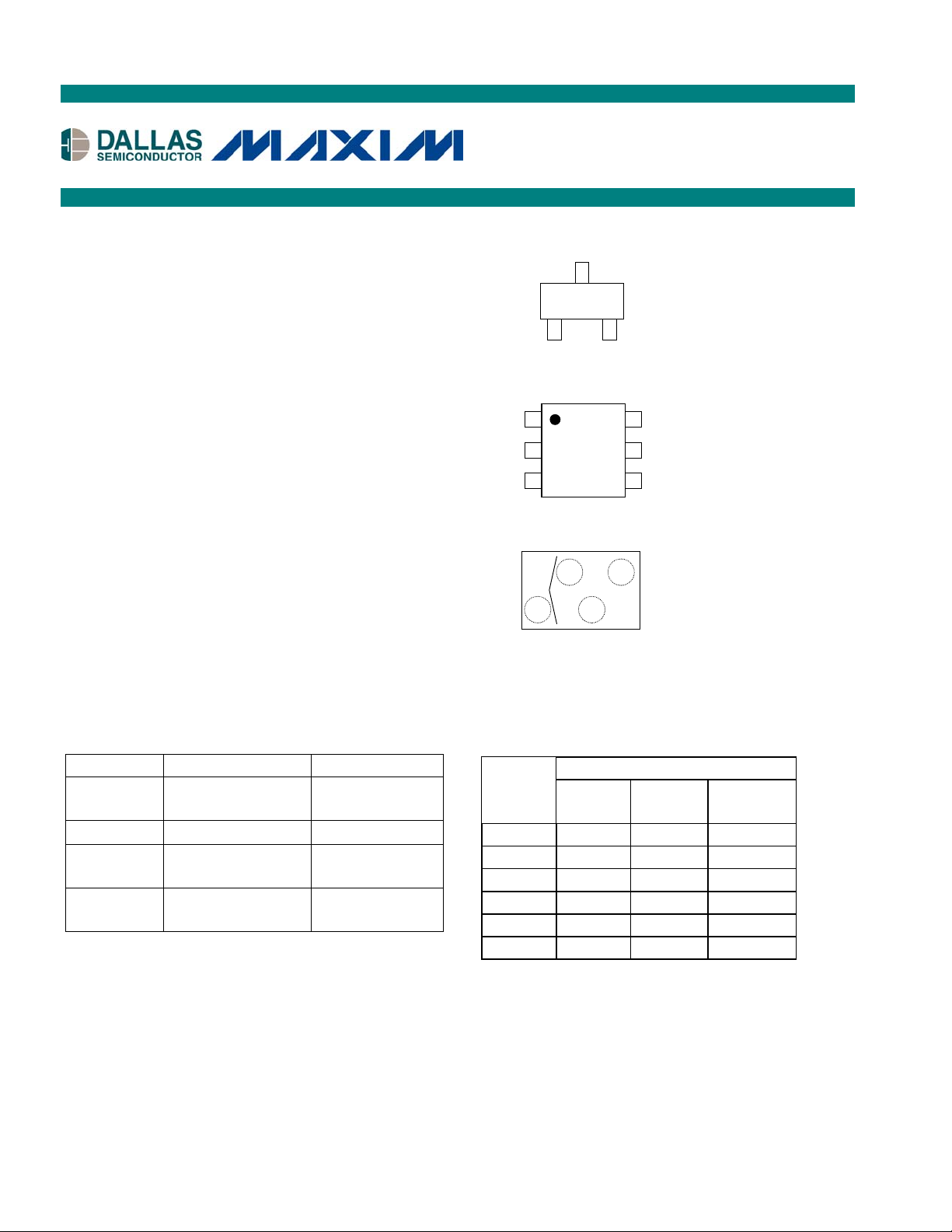
PIN CONFIGURATION
3
1
SOT23-3, Top View
1
2
3
TSOC, Top View
1
2
AB
Flip Chip, Top view, bumps
not visible
2
6
5
4
ORDERING INFORMATION
PART TEMP RANGE PACKAGE
DS2411R/
T&R
DS2411P
DS2411P/
T&R
DS2411X
-40°C to +85°C
-40°C to +85°C
-40°C to +85°C
-40°C to +85°C
SOT23-3,
Tape-and-Reel
TSOC
TSOC,
Tape-and-Reel
Flip Chip,
Tape-and-Reel
PIN DESCRIPTION
PIN
NAME
SOT23 TSOC
I/O 1 2 A1
V
CC
26B2
GND 3 1 B1
N.C. — 3 A2
N.C. — 4 —
FLIP
CHIP
N.C. — 5 —
DESCRIPTION
The DS2411 silicon serial number is a low-cost, electronic registration number with external power
supply. It provides an absolutely unique identity that can be determined with a minimal electronic
interface (typically, a single port pin of a microcontroller). The DS2411’s registration number is a
factory-lasered, 64-bit ROM that includes a unique 48-bit serial number, an 8-bit CRC, and an 8-bit
family code (01h). Data is transferred serially through the Dallas Semiconductor’s 1-Wire protocol. The
external power supply is required, extending the operating voltage range of the device below typical
1-Wire devices.
1-Wire is a registered trademark of Dallas Semiconductor. 1 of 11 052003
Page 2

DS2411
ABSOLUTE MAXIMUM RATINGS*
I/O Voltage to GND -0.5V to +6V
VCC Voltage to GND -0.5V to +6V
I/O, VCC Current ±20mA
Operating Temperature Range -40°C to +85°C
Junction Temperature +150°C
Storage Temperature Range -55°C to +125°C
Soldering Temperature See IPC/JEDEC J-STD-
020A Specification
* This is a stress rating only and functional operation of the device at these or any other conditions above
those indicated in the operation sections of this specification is not implied. Exposure to absolute
maximum rating conditions for extended periods of time may affect reliability.
ELECTRICAL CHARACTERISTICS (VCC = 1.5V to 5.25V; TA = -40°C to +85°C.)
PARAMETER SYMBOL CONDITIONS MIN MAX UNITS
Operating Temperature T
Supply Voltage V
A
CC
(Note 1) -40 +85
(Note 1) 1.5 5.25 V
1-Wire Pullup VCC = V
I/O PIN GENERAL DATA
1-Wire Pullup Resistance R
Power-Up Delay t
PWRP
Input Capacitance C
Input Load Current I
Standby Supply Current I
Active Supply Current I
High-to-Low Switching
Threshold
V
Input Low Voltage V
Input High Voltage V
Low-to-High Switching
Threshold
V
Switching Hysteresis V
Output Low Voltage at 4mA V
Rising Edge Holdoff t
PUP
IO
L
CCS
CCA
TL
IL
IH
TH
HY
OL
REH
(Notes 1, 2) 0.3 2.2
V
stable to first
CC
1-Wire command (Notes 1, 3)
(Note 3) 100 pF
0V ≤ V(I/O) ≤ V
V(I/O) ≤ VIL, or V(I/O) ≥ V
(Notes 3, 4, 5) 0.4 3.2 V
(Note 1) 0.30 V
(Note 1)
(Notes 3, 4, 6) 0.75 3.4 V
(Notes 3, 7) 0.18 V
(Note 8) 0.4 V
Standard speed (Note 9, 3) 1.25 5
Overdrive speed (Note 9, 3) 0.5 2
Standard speed,
R
= 2.2kW (Note 1)
PUP
Recovery Time t
REC
Overdrive speed,
R
= 2.2kW (Note 1)
PUP
Overdrive speed, directly prior to
reset pulse; R
Standard speed 65
SLOT
Overdrive V
Overdrive V
(Note 1) 1.5 5.25 V
PUP
1200 µs
CC
IH
-1 +1 µA
1 µA
100 µA
-
V
CC
0.3
5
2
= 2.2kW (Note 1)
PUP
≥ 2.2V 8Timeslot Duration t
CC
≥ 1.5V 10
CC
5
°C
kW
V
µs
µs
µs
2 of 11
Page 3

PARAMETER SYMBOL CONDITIONS MIN MAX UNITS
L
L
I/O PIN, 1-Wire RESET, PRESENCE DETECT CYCLE
Reset Low Time t
RSTL
Standard speed 480 640
Overdrive speed 60 80
Standard speed 15 60
PDH
Overdrive V
Overdrive V
≥ 2.2V 2 6Presence-Detect High Time t
CC
≥ 1.5V 2 8.5
CC
Standard speed 60 240
Presence-Detect Low Time t
Presence-Detect Fall Time t
Presence-Detect Sample
Time
PDL
FPD
t
MSP
Overdrive V
Overdrive V
≥ 2.2V 8 24
CC
≥ 1.5V 8 30
CC
Standard speed (Note 10, 3) 0.4 8
Overdrive speed (Note 10, 3) 0.05 1
Standard speed (Note 1) 60 75
Overdrive V
Overdrive V
≥ 2.2V (Note 1) 6 10
CC
≥ 1.5V (Note 1) 8.5 10
CC
I/O PIN, 1-Wire WRITE
Standard speed (Notes 1, 13) 60 120
Write-0 Low Time t
W0L
Overdrive V
13)
Overdrive V
≥ 2.2V (Notes 1,
CC
≥ 1.5V (Notes 1,
CC
13)
Write-1 Low Time t
W1L
Standard speed (Notes 1, 11, 13) 5
Overdrive speed (Notes 1, 11, 13) 1
I/O PIN, 1-Wire READ
Read Low Time t
Read Sample Time t
RL
MSR
Standard speed (Notes 1, 11) 5
Overdrive speed (Notes 1, 11) 1
Standard speed (Notes 1, 12)
Overdrive speed (Notes 1, 12)
616
816
15 - e
2 - e
15 - e
2 - e
t
+ d
R
t
+ d
R
15
2
DS2411
µs
µs
µs
µs
µs
µs
µs
µs
µs
Note 1: System requirement.
Note 2: Maximum allowable pullup resistance is a function of the number of 1-Wire devices in the
system and 1-Wire recovery times. The specified value here applies to systems with only
one device and with the minimum 1-Wire recovery times. For more heavily loaded
systems, an active pullup such as that found in the DS2480B may be required. Minimum
allowable pullup resistance is slightly greater than the value necessary to produce the
absolute maximum current (20mA) during 1-Wire low times at V
V
= 0V.
OL
= 5.25V assuming
PUP
Note 3: Not production tested.
Note 4: V
and VTH are functions of VCC and temperature.
TL
Note 5: Voltage below which during a falling edge on I/O, a logic ‘0’ is detected.
Note 6: Voltage above which during a rising edge on I/O, a logic ‘1’ is detected.
Note 7: After V
is crossed during a rising edge on I/O, the voltage on I/O has to drop by VHY to
TH
be detected as logic ‘0’.
Note 8: The I-V characteristic is linear for voltages less than 1V.
Note 9: The earliest recognition of a negative edge is possible at t
after VTH has been reached
REH
on the previous edge.
Note 10: Interval during the negative edge on I/O at the beginning of a presence-detect pulse
between the time at which the voltage is 90% of V
10% of V
PUP
.
3 of 11
and the time at which the voltage is
PUP
Page 4

DS2411
(
)
Note 11: e represents the time required for the pullup circuitry to pull the voltage on I/O up VIL to
VTH.
Note 12: d represents the time required for the pullup circuitry to pull the voltage on I/O up from
VIL to the input-high threshold of the bus master.
Note 13: Interval begins when the voltage drops below VTL during a negative edge on I/O and ends
when the voltage rises above V
during a positive edge on I/O.
TH
OPERATION
The DS2411’s registration number is accessed through a single data line. The 48-bit serial number, 8-bit
family code, and 8-bit CRC are retrieved using the Dallas 1-Wire protocol. This protocol defines bus
transactions in terms of the bus state during specified time slots that are bus-master-generated falling
edges on the I/O pin. All data is read and written least significant bit first. The device requires a delay
between VCC power-up and initial 1-Wire communication, t
(1200ms). During this time the device
PWRP
may issue presence-detect pulses.
1-Wire BUS SYSTEM
The 1-Wire bus has a single bus master and one or more slaves. In all instances, the DS2411 is a slave
device. The bus master is typically either a microcontroller or a Dallas Semiconductor bridge chip such as
the DS2480, DS2490, or DS1481. The discussion of this bus system is broken down into three topics:
hardware configuration, transaction sequence, and 1-Wire signaling (signal type and timing).
Hardware Configuration
The 1-Wire bus has a single data line, I/O. It is important that each device on the bus be able to drive I/O
at the appropriate time. To facilitate this, each device has an open-drain or three-state output. The
DS2411 has an open-drain output with an internal circuit equivalent to that shown in Figure 3. The bus
master can have the same equivalent circuit. If a bidirectional pin is not available on the master, separate
output and input pins can be connected together. The bus requires a pullup resistor at the master end of
the bus, as shown in Figure 4. A multidrop bus consists of a 1-Wire bus with multiple slaves attached.
The 1-Wire bus has a maximum data rate of 15.4kbps in standard speed and 125kbps in overdrive.
The idle state for the 1-Wire bus is high. If a transaction needs to be suspended for any reason, I/O must
remain high if the transaction is to be resumed. If the bus is pulled low, slave devices on the bus will
interpret the low as either a timeslot, or a reset depending on the duration.
Figure 1. DS2411 REGISTRATION NUMBER
MSB LSB
8-BIT CRC CODE 48-BIT SERIAL NUMBER 8-BIT FAMILY CODE
01h
MSB LSB MSB LSB MSB LSB
4 of 11
Page 5

Figure 2. 1-WIRE CRC GENERATOR
T
m
A
m
A
D
POLYNOMIAL = X8 + X5 + X4 + 1
DS2411
STAGE
0
X
1st
STAGE
1
X
2nd
STAGE
2
X
3rd
STAGE
3
X
4th
STAGE
4
X
5th
Figure 3. DS2411 EQUIVALENT CIRCUIT
V
CC
Rx
Tx
100 Ω
MOSFE
GROUND
STAGE
5
X
6th
6
X
7th
STAGE
STAGE
7
X
8th
8
X
INPUT DATA
I/O
£I
1
L
£
-1
Figure 4. BUS MASTER CIRCUIT
a) Open Drain b) DS2480B Serial Bridge
V
to DS2411
CC
BUS MASTER
DS5000 OR 8051
R
Rx
Tx
R
must be between 0.3 kW and 2.2 kW. The optimal
PUP
value depends on the 1-Wire communication speed and
the bus load characteristics.
OPEN-DRAIN
PORT PIN
PUP
I/O to DS2411
Ground to DS2411
5 of 11
UART
OR µC
* ONLY ONE DS9502 ESD PROTECTION DIODE WITH 5V
SIN (RxD)
SOUT (TxD)
LM
START
5V
1
0
STOP
5V OPERATION ONLY
V
DD
POL
V
PP
1-W
RxD
DS2480
TxD
GND
V
I/O
cc
*
GN
Page 6

DS2411
TRANSACTION SEQUENCE
The communication sequence for accessing the DS2411 through the 1-Wire bus is as follows:
§ Initialization
§ ROM Function Command
§ Read Data
INITIALIZATION
All transactions on the 1-Wire bus begin with an initialization sequence. The initialization sequence
consists of a reset pulse transmitted by the bus master followed by a presence pulse(s) transmitted by the
slave(s). The presence pulse lets the bus master know that the DS2411 is on the bus and is ready to
operate. For more details, see the 1-Wire Signaling section.
ROM FUNCTION COMMANDS
Once the bus master has detected a presence, it can issue one of the three ROM function commands. All
ROM function command codes are 1 byte long. A list of these commands follows (see the flowchart in
Figure 5).
Read ROM [33h]
This command allows the bus master to read the DS2411’s 8-bit family code, unique 48-bit serial
number, and 8-bit CRC. This command should only be used if there is a single slave device on the bus. If
more than one slave is present on the bus, a data collision results when all slaves try to transmit at the
same time (open drain produces a wired-AND result), and the resulting registration number read by the
master will be invalid.
Search ROM [F0h]
When a system is initially brought up, the bus master might not know the number of devices on the
1-Wire bus or their registration numbers. By taking advantage of the wired-AND property of the bus, the
master can use a process of elimination to identify the registration numbers of all slave devices. For each
bit of the registration number, starting with the least significant bit, the bus master issues a triplet of time
slots. On the first slot, each slave device participating in the search outputs the true value of its
registration number bit. On the second slot, each slave device participating in the search outputs the
complemented value of its registration number bit. On the third slot, the master writes the true value of
the bit to be selected. All slave devices that do not match the bit written by the master stop participating
in the search. If both of the read bits are zero, the master knows that slave devices exist with both states of
the bit. By choosing which state to write, the bus master branches in the romcode tree. After one complete
pass, the bus master knows the registration number of a single device. Additional passes identify the
registration numbers of the remaining devices. Refer to App Note 187: 1-Wire Search Algorithm for a
detailed discussion, including an example.
Overdrive Skip ROM [3Ch]
This command causes all overdrive-capable slave devices on the 1-Wire network to enter overdrive speed
(OD = 1). All communication following this command has to occur at overdrive speed until a reset pulse
of minimum 480ms duration resets all devices on the bus to regular speed (OD = 0).
To subsequently address a specific overdrive-supporting device, a reset pulse at overdrive speed has to be
issued followed by a read ROM or search ROM command sequence. Overdrive speeds up the time for the
search process.
6 of 11
Page 7

Figure 5. ROM FUNCTIONS FLOW CHART
Y
Y
Y
Y
Y
Y
Y
Bus Master Tx
Reset Pulse
DS2411
Bus Master Tx ROM
Function Command
33h
Read ROM
Command?
DS2411 Tx
Family Code
(1 Byte)
OD
Reset Pulse ?
DS2411 Tx
Presence Pulse
N
N
F0h
Search ROM
Command?
DS2411 Tx Bit 0
DS2411 Tx Bit 0
Master Tx Bit 0
Bit 0
Match?
N
OD = 0
N
3Ch
OD Skip
Command?
OD = 1
N
DS2411 Tx
Serial Number
(6 Bytes)
DS2411 Tx
CRC Byte
DS2411 Tx Bit 1
DS2411 Tx Bit 1
Master Tx Bit 1
N
N
Bit 1
Match?
DS2411 Tx Bit 63
DS2411 Tx Bit 63
Master Tx Bit 63
Bit 63
Match?
7 of 11
Page 8

DS2411
1-WIRE SIGNALING
The DS2411 requires strict protocols to ensure data integrity. The protocol consists of four types of
signaling on one line: Reset Sequence with Reset Pulse and Presence Pulse, Write 0, Write 1, and Read
Data. Except for the presence pulse the bus master initiates all these signals. The DS2411 can
communicate at two different speeds: standard speed and Overdrive speed. If not explicitly set into the
Overdrive mode, the DS2411 will communicate at standard speed. While in Overdrive Mode the fast
timing applies to all waveforms.
To get from idle to active, the voltage on the 1-Wire line needs to fall from V
To get from active to idle, the voltage needs to rise from V
V
is relevant for the DS2411 when determining a logical level, but not for triggering any events.
ILMAX
past the threshold VTH. The voltage
ILMAX
below the threshold VTL.
PUP
The initialization sequence required to begin any communication with the DS2411 is shown in Figure 6.
A Reset Pulse followed by a Presence Pulse indicates the DS2411 is ready to receive data, given the
correct ROM and memory function command. In a mixed population network, the reset low time t
RSTL
needs to be long enough for the slowest 1-Wire slave device to recognize it as a reset pulse. If the bus
master uses slew-rate control on the falling edge, it must pull down the line for t
for the edge. A t
standard speed. If the DS2411 is in Overdrive Mode and t
duration of 480µs or longer will exit the Overdrive Mode returning the device to
RSTL
is no longer than 80µs, the device will
RSTL
+ tF to compensate
RSTL
remain in Overdrive Mode.
After the bus master has released the line it goes into receive mode (RX). Now, the 1-Wire bus is pulled
to V
VTH is crossed, the DS2411 waits for t
t
PDL
The t
expired, the DS2411 is ready for data communication. In a mixed population network, t
via the pullup resistor or, in case of a DS2480B driver, by active circuitry. When the threshold
PUP
and then transmits a Presence Pulse by pulling the line low for
PDH
. To detect a presence pulse, the master must test the logical state of the 1-Wire line at t
window must be at least the sum of t
RSTH
PDHMAX
, t
PDLMAX
, and t
RECMIN
. Immediately after t
.
MSP
should be
RSTH
RSTH
is
extended to minimum 480µs at standard speed and 48µs at Overdrive speed to accommodate other 1Wire devices.
Read/Write Time Slots
Data communication with the DS2411 takes place in time slots that carry a single bit each. Write time
slots transport data from bus master to slave. Read time-slots transfer data from slave to master. The
definitions of the write and read time slots are illustrated in Figure 7.
All communication begins with the master pulling the data line low. As the voltage on the 1-Wire line
falls below the threshold V
, the DS2411 starts its internal timing generator that determines when the
TL
data line will be sampled during a write time slot and how long data will be valid during a read time slot.
Master to Slave
For a write-one time slot, the voltage on the data line must have crossed the V
write-one low time t
below the V
THMIN
W1LMAX
threshold until the write-zero low time t
communication the voltage on the data line should not exceed V
After the V
threshold has been crossed, the DS2411 needs a recovery time t
THMAX
is expired. For a write-zero time slot, the voltage on the data line must stay
W0LMIN
is expired. For most reliable
during the entire t
ILMAX
the next time slot.
8 of 11
threshold after the
THMAX
W0L
before it is ready for
REC
window.
Page 9

INITIALIZATION PROCEDURE
Figure 6. Reset and Presence Pulse
MASTER Tx RESET PULSE MASTER Rx PRESENCE PULSE
e
V
IHMA STER
V
V
PUP
V
TH
V
ILM AX
TL
0V
t
F
t
RSTL
RESISTOR MASTER DS2411
READ/WRITE TIMING DIAGRAM
Figure 7a. Write-One Time Slot
t
W1L
e
V
IHMA STE R
V
V
PUP
V
V
ILMAX
0V
TH
TL
t
F
t
PDH
t
MSP
t
PDL
t
RSTH
t
SLOT
t
DS2411
REC
RESISTOR MASTER DS2411
Figure 7b. Write-Zero Time Slot
t
W0L
V
IHM AS TER
V
V
PUP
V
V
ILMA X
TH
TL
0V
t
F
RESISTOR MASTER DS2411
Figure 7c. Read-data Time Slot
t
MSR
MASTER
SAMPLING
WINDOW
V
IHM AS TE R
V
V
PUP
V
V
ILMA X
0V
TH
t
RL
TL
t
F
d
t
SLOT
t
REC
t
SLOT
t
REC
RESISTOR MASTER DS2411
9 of 11
Page 10

DS2411
Slave to Master
A read-data time slot begins like a write-one time slot. The voltage on the data line must remain below
V
DS2411 will start pulling the data line low; its internal timing generator determines when this pull-down
ends and the voltage starts rising again. When responding with a 1, the DS2411 will not hold the data line
low at all, and the voltage starts rising as soon as t
until the read low time tRL is expired. During the tRL window, when responding with a 0, the
TLMIN
is over.
RL
The sum of t
side define the master sampling window (t
+ d (rise rime) on one side and the internal timing generator of the DS2411 on the other
RL
MSRMIN
to t
MSRMAX
) in which the master must perform a read
from the data line. For most reliable communication, tRL should be as short as permissible and the master
should read close to but no later than t
t
is expired. This guarantees sufficient recovery time t
SLOT
MSRMAX
. After reading from the data line, the master must wait until
for the DS2411 to get ready for the next
REC
time slot.
Improved Network Behavior
In a 1-Wire environment, line termination is possible only during transients controlled by the bus master
(1-Wire driver). 1-Wire networks therefore are susceptible to noise of various origins. Depending on the
physical size and topology of the network, reflections from end points and branch points can add up or
cancel each other to some extent. Such reflections are visible as glitches or ringing on the 1-Wire
communication line. A glitch during the rising edge of a time slot can cause a slave device to lose
synchronization with the master and, as a consequence, result in a search ROM command coming to a
dead end. For better performance in network applications, the DS2411 uses a new 1-Wire front end,
which makes it less sensitive to noise and also reduces the magnitude of noise injected by the slave
device itself.
The 1-Wire front end of the DS2411 differs from traditional slave devices in four characteristics.
1) The falling edge of the presence pulse has a controlled slew rate. This provides a better match to the
line impedance than a digitally switched transistor, converting the high frequency ringing known from
traditional devices into a smoother low-bandwidth transition. The slew rate control is specified by the
parameter t
2) There is additional low-pass filtering in the circuit that detects the falling edge at the beginning of a
time slot. This reduces the sensitivity to high-frequency noise. As a consequence, the duration of the
setup time t
not apply at Overdrive speed.
3) There is a hysteresis at the low-to-high switching threshold V
doesn’t go below VTH - VHY, it will not be recognized (Figure 8, Case A). The hysteresis is effective
at any 1-Wire speed.
4) There is a time window specified by the rising edge hold-off time t
ignored, even if they extend below VTH - VHY threshold (Figure 8, Case B, tGL < t
droops or glitches that appear late after crossing the V
window cannot be filtered out and will be taken as beginning of a new time slot (Figure 8, Case C, t
³ t
). The duration of the hold-off time is independent of the 1-Wire speed.
REH
Only devices which have the parameters t
the improved 1-Wire front end.
, which has different values for standard and Overdrive speed.
FPD
at standard speed is larger than with traditional devices. This additional filtering does
SU
. If a negative glitch crosses VTH but
TH
during which glitches will be
REH
). Deep voltage
REH
threshold and extend beyond the t
TH
, VHY and t
FPD
specified in their electrical characteristics use
REH
REH
GL
10 of 11
Page 11

DS2411
NOISE SUPPRESSION SCHEME Figure 8
t
V
PUP
V
TH
V
HY
Case A Case CCase B
0V
REH
t
GL
t
REH
t
GL
CRC GENERATION
To validate the registration number transmitted from the DS2411, the bus master can generate a CRC
value from the 8-bit family code and unique 48-bit serial number as it is received. If the CRC matches the
last 8 bits of the registration number, the transmission is error free.
The equivalent polynomial function of this CRC is: CRC = x8 + x5 + x4 + 1.
CUSTOM DS2411
Customization of a portion of the unique 48-bit serial number by the customer is available. Dallas
Semiconductor will register and assign a specific customer ID in the 12 most significant bits of the 48-bit
field. The next most significant bits are selectable by the customer as a starting value, and the least
significant bits are non-selectable and will be automatically incremented by one. Certain quantities and
conditions apply for these custom parts. Contact your Maxim/Dallas Semiconductor sales representative
for more information.
11 of 11
 Loading...