

Page 1
N
www.maxim-ic.com
DS2404
EconoRAM Time Chip
FEATURES
§ 4096 bits of nonvolatile dual-port memory
including real time clock/calendar in binary
format, programmable interval timer, and
programmable power-on cycle counter
®
§ 1-Wire
interface for MicroLAN
communication at 16.3kbits/s
§ 3-wire host interface for high-speed data
communications at 2Mb/s
§ Unique, factory-lasered and tested 64-bit
registration number (8-bit family code +
48-bit serial number + 8-bit CRC tester)
assures absolute traceability because no two
parts are alike
§ Memory partitioned into 16 pages of 256-bits
for packetizing data
§ 256-bit scratchpad with strict read/write
protocols ensures integrity of data transfer
§ Programmable alarms can be set to generate
interrupts for interval timer, real time clock,
and/or cycle counter
§ 16-pin DIP, SO, and SSOP packages
§ Operating temperature range from -40°C to
+85°C
§ Operating voltage range from 2.8V to 5.5V
ORDERING INFORMATION
DS2404-001 16-pin DIP
DS2404S-001 16-pin SO
DS2404B 16-pin SSOP
DS2404S-001/T&R Tape and Reel of S2404S-001
DS2404B/T&R Tape and Reel of DS2404B
PIN ASSIGNMENT
VCC 1 16 VCC
IRQ 2 15 X1
RST 3 14 X2
DQ 4 13 GND
I/O 5 12 NC
CLK 6 11 1HZ
C 7 10VBATO
GND 8 9 VBATB
16-PIN DIP (300 MIL)
16-PIN SO (300 MIL)
16-PIN SSOP (208 MIL)
See Mechanical Drawings Section
PIN DESCRIPTION
VCC – 2.8 to 5.5V
IRQ – Interrupt Output
RST – 3-Wire Reset Input
DQ – 3-Wire Input/Output
I/O – 1-Wire Input/Output
CLK – 3-Wire Clock Input
NC – No Connection
GND – Ground
V
– Battery Backup Input
BATB
V
1Hz – 1Hz Output
X1, X2 – Crystal Connections
– Battery Operate Input
BATO
DESCRIPTION
The DS2404 EconoRAM Time Chip offers a simple solution for storing and retrieving vital data and time
information with minimal hardware. The DS2404 contains a unique lasered ROM, real-time
clock/calendar, interval timer, cycle counter, programmable interrupts, and 4096-bits of SRAM. Two
separate ports are provided for communication: 1-Wire and 3-wire. Using the 1-Wire port, only one pin is
required for communication, and the lasered-ROM can be read even when the DS2404 is without power.
The 3-wire port provides high-speed communication using the traditional Dallas Semiconductor 3-wire
interface. With either interface, a strict protocol for accessing the DS2404 ensures data integrity. Utilizing
backup energy sources, the data is nonvolatile (NV) and allows for stand-alone operation.
1 of 29 110501
Page 2

DS2404
The DS2404 features can be used to create a stopwatch, alarm clock, time and date stamp, logbook, hour
meter, calendar, system power-cycle timer, expiration timer, and event scheduler.
DETAILED PIN DESCRIPTION
PIN SYMBOL DESCRIPTION
1,16 V
2
3
CC
IRQ
RST
4DQData input/output pin for 3-wire operation.
5I/OData input/output for 1-Wire operation: Open drain. (See “Parasite
6CLKClock input pin for 3-wire operation.
7,12 NC
8,13 GND Ground pin. Either pin can be used for ground.
9V
10 V
BATB
BATO
11 1Hz 1Hz square wave output: Open drain.
14,15 X1,X
2
Power input pins for V
one can be used for V
V
pin description and “Power Control” section).
BATO
operate mode. 2.8V to 5.5V operation. Either
CC
Only one is required for normal operation. (See
CC.
Interrupt output pin. Open drain.
Reset input pin for 3-wire operation. (See “Parasite Power” section.)
Power” section.)
No connection pins.
Battery backup input pin. Battery voltage can be 2.8V to 5.5V. (See
V
Battery operate input pin for 2.8V to 5.5V operation. The V
V
pin description and “Power Control” section.)
BATO
pins must be grounded when this pin is used to power the chip.
BATB
CC
&
(See “Power Control” section.)
Crystal pins. Connections for a standard 32.768kHz quartz crystal,
EPSON part number C-002RX or C-004R (be sure to request 6pF load
capacitance).
NOTE: X1 and X2 are very high impedance nodes. It is recommended
that they and the crystal be guard-ringed with ground and that high
frequency signals be kept away from the crystal area. See Figure 18 and
Application Note 58 for details.
OVERVIEW
The DS2404 has four main data components: 1) 64-bit lasered ROM, 2) 256-bit scratchpad, 3) 4096-bit
SRAM, and 4) timekeeping registers. The timekeeping section utilizes an on-chip oscillator that is
connected to an external 32.768kHz crystal. The SRAM and timekeeping registers reside in one
contiguous address space referred to hereafter as memory. All data is read and written least significant bit
first.
Two communication ports are provided a 1-Wire port and a 3-wire port. A port selector determines which
of the two ports is being used. The communication ports and the ROM are parasite-powered via I/O,
RST , or V
through the 1-Wire port. The scratchpad and memory are accessible via either port.
If the 3-wire port is used, the master provides one of four memory function commands: 1) read memory,
2) read scratchpad, 3) write scratchpad, or 4) copy scratchpad. The only way to write memory is to first
write the scratchpad and then copy the scratchpad data to memory. (See Figure 6.)
If the 1-Wire port is used, the memory functions will not be available until the ROM function protocol
has been established. This protocol is described in the ROM functions flow chart (Figure 9). The master
must first provide one of five ROM function commands: 1) read ROM, 2) match ROM, 3) search ROM,
. This allows the ROM to be read in the absence of power. The ROM data is accessible only
CC
2 of 29
Page 3
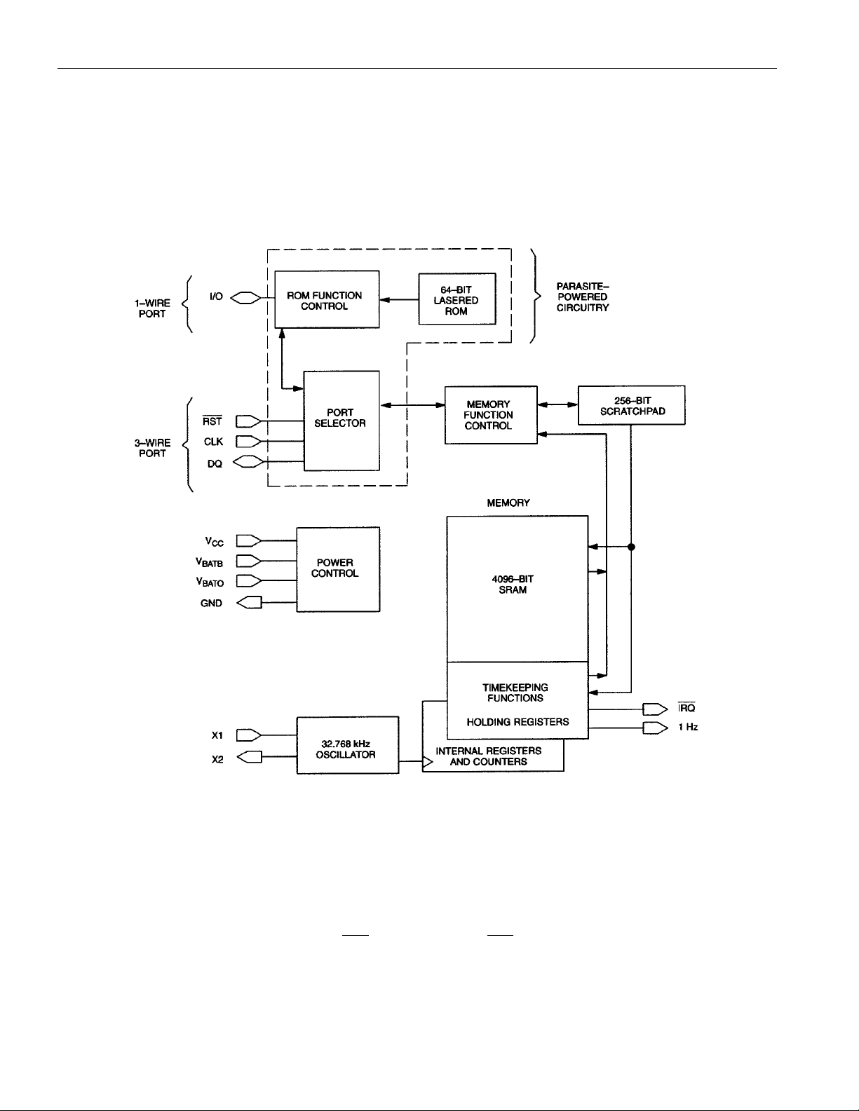
DS2404
4) skip ROM or 5) search interrupt. After a ROM function sequence has been successfully executed, the
memory functions are accessible and the master may then provide any one of the four memory function
commands (Figure 6).
The “Power Control” section provides for two basic power configurations: battery operate mode and V
operate mode. The battery operate mode utilizes one supply connected to V
may utilize two supplies; the primary supply connects to VCC and a backup supply connects to V
. The VCC operate mode
BATO
BATB
.
DS2404 BLOCK DIAGRAM Figure 1
CC
COMMUNICATION PORTS
Two communication ports are provided: a 1-Wire and a 3-wire port. The advantages of using the 1-Wire
port are as follows: 1) provides access to the 64-bit lasered ROM, 2) consist of a single communication
signal (I/O), and 3) multiple devices may be connected to the 1-Wire bus. The 1-Wire bus has a
maximum data rate of 16.3kbits/s and requires one 5kW external pull-up.
The 3-wire port consists of three signals: RST , CLK, and DQ. RST is an enable input, DQ is bidirectional
serial data, and the CLK input is used to clock in or out the serial data. The advantages of using the
3-wire port are 1) high data transfer rate (2MHz), 2) simple timing, and 3) no external pull-up required.
3 of 29
Page 4
DS2404
Port selection is accomplished on a first-come, first-serve basis. Whichever port comes out of reset first
will obtain control. For the 3-wire port, this is done by bringing RST high. For the 1-Wire port, this is
done on the first falling edge of I/O after the reset and presence pulses. (See “1-Wire Signaling” section.)
More information on how to arbitrate port access is found in section “Device Operation Modes” later in
this document.
PARASITE POWER
The block diagram (Figure 1) shows the parasite-powered circuitry. This circuitry “steals” power
whenever the I/O, RST , or VCC pins are high. When using the 1-Wire port in battery operate mode,
RST and V
provide no power since they are low. However, I/O will provide sufficient power as long as
CC
the specified timing and voltage requirements are met. The advantages of parasite power are two-fold:
1) by parasiting off these pins, battery power is conserved and 2) the ROM may be read in absence of
normal power. For instance, in battery-operate mode, if the battery fails, the ROM may still be read
normally.
In battery-backed mode, if VCC fails, the port switches in the battery but inhibits communication. The
ROM may still be read normally over the 1-Wire port if RST is low.
64-BIT LASERED ROM
Each DS2404 contains a unique ROM code that is 64 bits long. The first eight bits are a 1-Wire family
code (DS2404 code is 04h). The next 48 bits are a unique serial number. The last eight bits are a CRC of
the first 56 bits. (See Figure 2.)
The 1-Wire CRC is generated using a polynomial generator consisting of a shift register and XOR gates
as shown in Figure 3. The polynomial is X8 + X5 + X4 + 1. Additional information about the Dallas
1-Wire Cyclic Redundancy Check is available in Application Note 27, “Understanding and Using Cyclic
Redundancy Checks with Dallas Semiconductor iButton Products”.
The shift register bits are initialized to zero. Then starting with the least significant bit of the family code,
one bit at a time is shifted in. After the 8th bit of the family code has been entered, then the serial number
is entered. After the 48th bit of the serial number has been entered, the shift register contains the CRC
value. Shifting in the eight bits of CRC should return the shift register to all zeros.
64-BIT LASERED ROM Figure 2
CRC SERIAL NUMBER DS2404 FAMILY CODE
8 BITS 48-BIT UNQUE NUMBER 04h
MSB LSB
1-WIRE CRC CODE Figure 3
4 of 29
Page 5
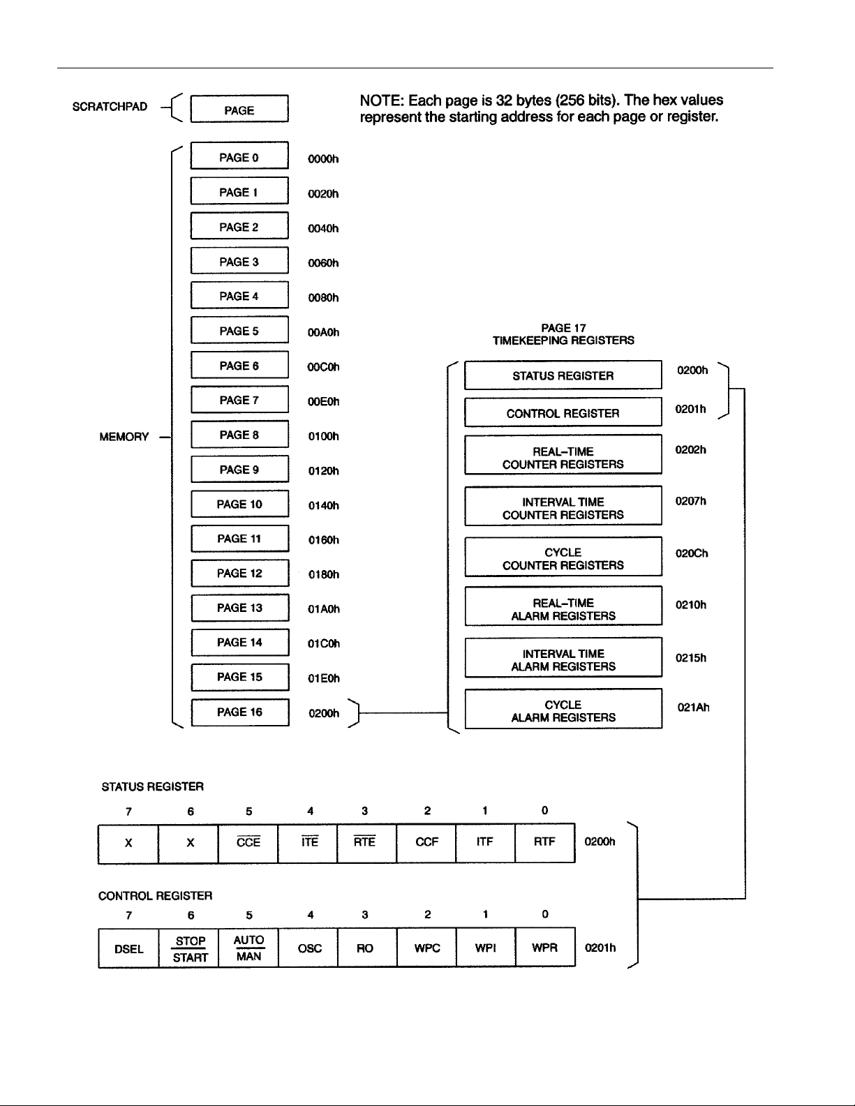
MEMORY MAP Figure 4
DS2404
5 of 29
Page 6

DS2404
MEMORY
The memory map in Figure 4 shows a page (32 bytes) called the scratchpad and 17 pages called memory.
Pages 0 through 15 each contain 32 bytes which make up the 4096-bit SRAM. Page 16 has only 30 bytes
which contain the timekeeping registers.
The scratchpad is an additional page of memory that acts as a buffer when writing to memory. Data is
first written to the scratchpad where it can be read back. After the data has been verified, a copy
scratchpad command will transfer the data to memory. This process ensures data integrity when
modifying the memory.
TIMEKEEPING
A 32.768kHz crystal oscillator is used as the time base for the timekeeping functions. The oscillator can
be turned on or off by an enable bit in the control register. The oscillator must be on for the real-time
clock, interval timer, cycle counter and 1Hz output to function.
The timekeeping functions are double buffered. This feature allows the master to read time or count
without the data changing while it is being read. To accomplish this, a snapshot of the counter data is
transferred to holding registers which the user accesses. This occurs after the eighth bit of the Read
Memory Function command.
Real-Time Clock
The real-time clock is a 5-byte binary counter. It is incremented 256 times per second. The least
significant byte is a count of fractional seconds. The upper four bytes are a count of seconds. The realtime clock can accumulate 136 years of seconds before rolling over. Time/date is represented by the
number of seconds since a reference point which is determined by the user. For example, 12:00A.M.,
January 1, 1970 could be a reference point.
Interval Timer
The interval timer is a 5-byte binary counter. When enabled, it is incremented 256 times per second. The
least significant byte is a count of fractional seconds. The interval timer can accumulate 136 years of
seconds before rolling over. The interval timer has two modes of operation which are selected by the
MANAUTO/ bit in the control register. In the auto mode, the interval timer will begin counting after the
I/O line has been high for a period of time determined by the DSEL bit in the control register. Similarly,
the interval timer will stop counting after the I/O line has been low for a period of time determined by the
DSEL bit. In the manual mode, time accumulation is controlled by the STARTSTOP/ bit in the control
register.
NOTE: For auto mode operation, the high level on the I/O pin must be greater than or equal to 70% of
V
CC
or V
BATO
.
Cycle Counter
The cycle counter is a 4-byte binary counter. It increments after the falling edge of the I/O line if the
appropriate I/O line timing has been met. This timing is selected by the DSEL bit in the control register.
(See “Status/ Control” section).
NOTE: For cycle counter operation, the high level on the I/O pin must be greater than or equal to 70% of
V
CC
or V
BATO
.
6 of 29
Page 7
DS2404
Alarm Registers
The alarm registers for the real-time clock, interval timer, and cycle counter all operate in the same
manner. When the value of a given counter equals the value in its associated alarm register, the
appropriate flag bit is set in the status register. If the corresponding interrupt enable bit(s) in the status
register is set, an interrupt is generated. If a counter and its associated alarm register are write protected
when an alarm occurs, access to the device becomes limited. (See “Status/Control”, “Interrupts”, and the
“Programmable Expiration” sections.)
STATUS/CONTROL REGISTERS
The status and control registers are the first two bytes of page 16 (see “Memory Map”, Figure 4).
Status Register
76543210
XX
CCE
ITE RTE
CCF ITF RTF 0200h
Don’t care bits Read Only
RTF Real-time clock alarm flag
0
ITF Interval timer alarm flag
1
CCF Cycle counter alarm flag
2
When a given alarm occurs, the corresponding alarm flag is set to a logic 1. The alarm flag(s) is cleared
by reading the status register.
RTE
3
4
ITE
5
CCE
Real-time interrupt enable
Interval timer interrupt enable
Cycle counter interrupt enable
Writing any of the interrupt enable bits to a logic 0 will allow an interrupt condition to be generated when
its corresponding alarm flag is set (see “Interrupts” section).
Control Register
76543210
DSEL
WPR Write protect real-time clock/alarm registers
0
WPI Write protect interval timer/alarm registers
1
WPC Write protect cycle counter/alarm registers
2
STOP
START
AUTO
MAN.
OSC RO WPC WPI WPR 0201h
7 of 29
Page 8

DS2404
Setting a write protect bit to a logic 1 will permanently write protect the corresponding counter and alarm
registers, all write protect bits, and additional bits in the control register. The write protect bits can not be
written in a normal manner (see “Write Protect/Programmable Expiration” section).
RO Read Only
3
If a programmable expiration occurs and the read only bit is set to a logic 1, then the DS2404 becomes
read only. If a programmable expiration occurs and the read only bit is a logic 0, then only the 64-bit
lasered ROM can be accessed (see “Write Protect/Programmable Expiration” section).
OSC Oscillator enable
4
This bit controls the crystal oscillator. When set to a logic 1, the oscillator will start operation. When the
oscillator bit is a logic 0, the oscillator will stop.
5
AUTO/ MAN Automatic/ Manual Mode
When this bit is set to a logic 1, the interval timer is in automatic mode. In this mode, the interval timer is
enabled by the I/O line. When this bit is set to a logic 0, the interval timer is in manual mode. In this
mode the interval timer is enabled by the STOP/START bit.
6
STOP/START
Stop/Start (in Manual Mode)
If the interval timer is in manual mode, the interval timer will start counting when this bit is set to a logic
0 and will stop counting when set to a logic 1. If the interval timer is in automatic mode, this bit has no
effect.
DSEL Delay Select Bit
7
This bit selects the delay that it takes for the cycle counter and the interval timer (in auto mode) to see a
transition on the I/O line. When this bit is set to a logic 1, the delay time is 123 + 2 ms. This delay allows
communication on the I/O line without starting or stopping the interval timer and without incrementing
the cycle counter. When this bit is set to a logic 0, the delay time is 3.5 ±0.5 ms.
MEMORY FUNCTION COMMANDS
The “Memory Function Flow Chart” (Figure 6) describes the protocols necessary for accessing the
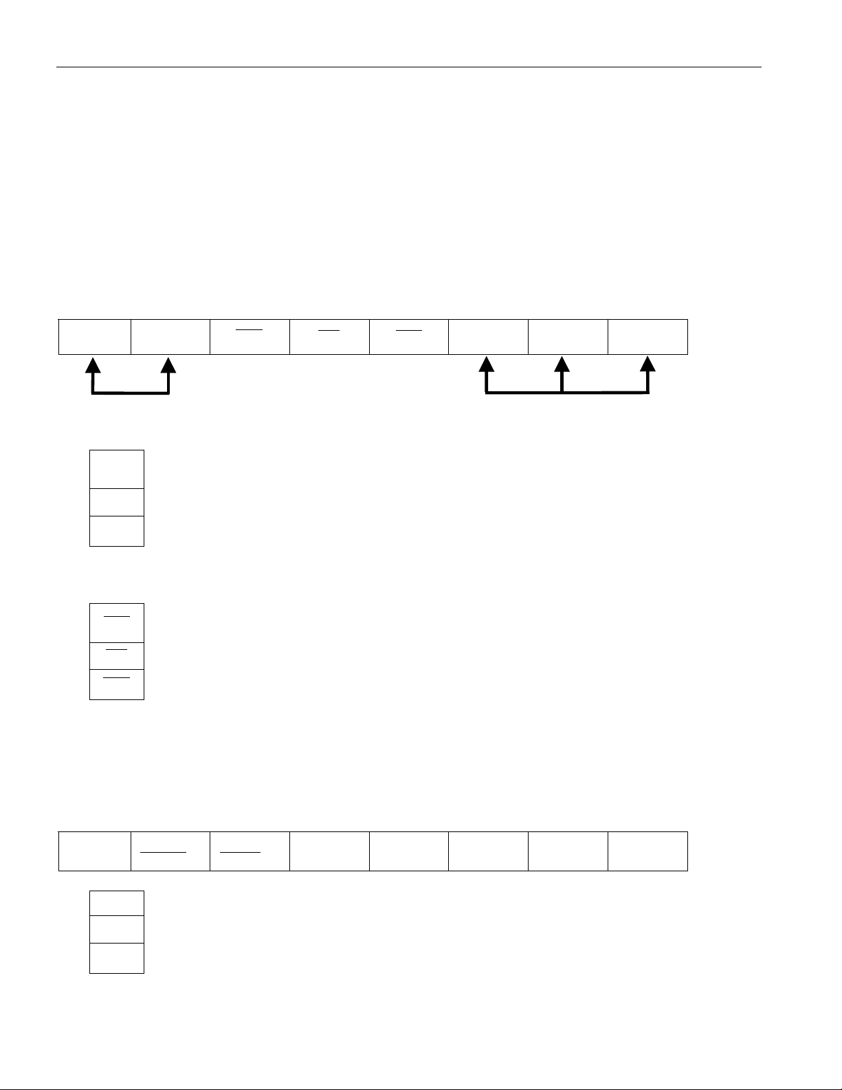
memory. Two examples follow the flowchart. Three address registers are provided as shown in Figure 5.
The first two registers represent a 16-bit target address (TA1, TA2). The third register is the ending
offset/data status byte (E/S).
The target address points to a unique byte location in memory. The first five bits of the target address
(T4:T0) represent the byte offset within a page. This byte offset points to one of 32 possible byte
locations within a given page. For instance, 00000b points to the first byte of a page where as 11111b
would point to the last byte of a page.
8 of 29
Page 9

DS2404
The third register (E/S) is a read only register. The first five bits (E4: E0) of this register are called the
ending offset. The ending offset is a byte offset within a page. Bit 5 (PF) is the partial byte flag. Bit 6
(OF) is the overflow flag. Bit 7 (AA) is the authorization accepted flag.
ADDRESS REGISTERS Figure 5
76543210
TARGET ADDRESS (TA1) T7 T6 T5 T4 T3 T2 T1 T0
TARGET ADDRESS (TA2) T15 T14 T13 T12 T11 T10 T9 T8
ENDING ADDRESS WITH
DATA STATUS (E/S)
(READ ONLY)
AA OF PF E4 E3 E2 E1 E0
Write Scratchpad Command [0Fh]
After issuing the write scratchpad command, the user must first provide the 2–byte target address,
followed by the data to be written to the scratchpad. The data will be written to the scratchpad starting at
the byte offset (T4:T0). The ending offset (E4: E0) will be the byte offset at which the host stops writing
data. The maximum ending offset is 11111b (31d). If the host attempts to write data past this maximum
offset, the overflow flag (OF) will be set and the remaining data will be ignored. If the user writes an
incomplete byte and an overflow has not occurred, the partial byte flag (PF) will be set.
Read Scratchpad Command [AAh]
This command may be used to verify scratchpad data and target address. After issuing the read scratchpad
command, the user may begin reading. The first two bytes will be the target address. The next byte will
be the ending offset/data status byte (E/S) followed by the scratchpad data beginning at the byte offset
(T4: T0). The user may read data until the end of the scratchpad after which the data read will be all logic
1’s.
Copy Scratchpad [55h]
This command is used to copy data from the scratchpad to memory. After issuing the copy scratchpad
command, the user must provide a 3-byte authorization pattern. This pattern must exactly match the data
contained in the three address registers (TA1, TA2, E/S, in that order). If the pattern matches, the AA
(Authorization Accepted) flag will be set and the copy will begin. At this point, the part will go into a T
mode, transmitting a logic 1 to indicate the copy is in progress. A logic 0 will be transmitted after the data
has been copied. Any attempt to reset the part will be ignored while the copy is in progress. Copy
typically takes 30 ms.
The data to be copied is determined by the three address registers. The scratchpad data from the
beginning offset through the ending offset, will be copied to memory, starting at the target address.
Anywhere from 1 to 32 bytes may be copied to memory with this command. Whole bytes are copied even
if only partially written. The AA flag will be cleared only by executing a write scratchpad command.
X
9 of 29
Page 10

MEMORY FUNCTION FLOW CHART Figure 6
DS2404
10 of 29
Page 11

DS2404
Read Memory [F0h]
The read memory command may be used to read the entire memory. After issuing the command, the user
must provide the 2-byte target address. After the two bytes, the user reads data beginning from the target
address and may continue until the end of memory, at which point logic 1’s will be read. It is important to
realize that the target address registers will contain the address provided. The ending offset/data status
byte is unaffected.
The hardware of the DS2404 provides a means to accomplish error-free writing to the memory section.
To safeguard reading data in the 1-Wire environment and to simultaneously speed up data transfers, it is
recommended to packetize data into data packets of the size of one memory page each. Such a packet
would typically store a 16-bit CRC with each page of data to ensure rapid, error-free data transfers that
eliminate having to read a page multiple times to determine if the received data is correct or not. (See the
Book of DS19xx iButton Standards, Chapter 7 for the recommended file structure to be used with the 1Wire environment.)
MEMORY FUNCTION EXAMPLES
Example 1: Write one page of data to page 15
Read page 15 (3-wire port)
MASTER MODE DATA(LSB FIRST) COMMENTS
TX Reset
TX 0Fh Issue “write scratchpad” command
TX E0h TA1, beginning offset=0
TX 01h TA2, address=01E0h
TX <32 data bytes> Write 1 page of data to scratchpad
TX Reset
TX AAh Issue “read scratchpad” command
RX E0h Read TA1, beginning offset=0
RX 01h Read TA2, address=01E0h
RX 1Fh Read E/S, ending offset=31d, flags=0
RX <32 data bytes> Read scratchpad data and verify
TX Reset
TX 55h Issue “copy scratchpad” command
TX E0h
TX 01h
TX 1Fh
RX <busy indicator>
TX Reset
TX F0h Issue “read memory” command
TX E0h TA1, beginning offset=0
TX 01h TA2, address=01E0h
RX <32 data bytes> Read memory page 15 and verify
TX Reset
Master pulses RST low
Master pulses RST low
Master pulses RST low
TA1
TA2 AUTHORIZATION CODE
E/S
Wait until DQ=0 (~30 ms typical)
Master pulses
Master pulses
RST low
RST low, done
NOTE: The ROM function commands do not apply to the 3-wire port. After RST is at a high level, the
device expects to receive a memory function command.
11 of 29
Page 12

DS2404
Example 2: Write two data bytes to memory locations 0026h and 0027h (the seventh and eighth byte of
page 1). Read entire memory (1-Wire port).
MASTER MODE DATA(LSB FIRST) COMMENTS
TX Reset
reset pulse (480–960 ms)
RX Presence presence pulse
TX CCh Issue “skip ROM” command
TX 0Fh Issue “write scratchpad” command
TX 26h TA1, beginning offset=6
TX 00h TA2, address=0026h
TX <2 data bytes> Write 2 bytes of data to scratchpad
TX Reset reset pulse
RX Presence presence pulse
TX CCh Issue “skip ROM” command
TX AAh Issue “read scratchpad” command
RX 26h Read TA1, beginning offset=6
RX 00h Read TA2, address=0026h
RX 07h Read E/S, ending offset=7, flags=0
RX <2 data bytes> Read scratchpad data and verify
TX Reset reset pulse
RX Presence presence pulse
TX CCh Issue “skip ROM” command
TX 55h Issue “copy scratchpad” command
TX 26h
TX 00h
TX 07h
TA1
TA2 AUTHORIZATION CODE
E/S
TX Reset reset pulse
RX Presence presence pulse
TX CCh Issue “skip ROM” command
TX F0h Issue “read memory” command
TX 00h TA1, beginning offset=0
TX 00h TA2, address=0000h
RX <542 bytes> Read entire memory
TX Reset reset pulse
RX Presence presence pulse, done
WRITE PROTECT/PROGRAMMABLE EXPIRATION
The write protect bits (WPR, WPI, WPC) provide a means of write protecting the timekeeping data and
limiting access to the DS2404 when an alarm occurs (programmable expiration).
The write protect bits may not be written by performing a single copy scratchpad command. Instead, to
write these bits, the copy scratchpad command must be performed three times. Please note that the AA bit
will be set, as expected, after the first copy command is successfully executed. Therefore, the
authorization pattern for the second and third copy command should have this bit set. The read
scratchpad command may be used to verify the authorization pattern.
12 of 29
Page 13

DS2404
The write protect bits, once set, permanently write protects their corresponding counter and alarm
registers, all write protect bits, and certain control register bits as shown in Figure 7. The time/count
registers will continue to count if the oscillator is enabled. If the user wishes to set more than one write
protect bit, the user must set them at the same time. Once a write protect bit is set it cannot be undone,
and the remaining write protect bits, if not set, cannot be set.
The programmable expiration takes place when one or more write protect bits have been set and a
corresponding alarm occurs. If the RO (read only) bit is set, only the read scratchpad and read memory
function commands are available. If the RO bit is a logic “0”, no memory function commands are
available. The ROM functions are always available.
WRITE PROTECT CHART Figure 7
WRITE PROTECT BIT SET: WPR WPI WPC
Data Protected from
User Modification:
* Becomes write “1” only, i.e., once written to a logic “1”, may not be written back to a logic “0”.
** Forced to a logic “0”.
Real Time Clock
Real Time Alarm
WPR
WPI
WPC
RO
OSC *
Interval Timer
Interval Time Alarm
WPR
WPI
WPC
RO
OSC *
STOP/START **
AUTO/ MAN
Cycle Counter
Cycle Counter Alarm
WPR
WPI
WPC
RO
OSC *
DSEL
1-WIRE BUS SYSTEM
The 1-Wire bus is a system which has a single bus master and one or more slaves. In most instances the
DS2404 behaves as a slave. The exception is when the DS2404 generates an interrupt due to a
timekeeping alarm. The discussion of this bus system is broken down into three topics: hardware
configuration, transaction sequence, and 1-Wire signaling (signal types and timing). The 1-Wire protocol
defines bus transactions in terms of the bus state during specific time slots that are initiated on the falling
edge of sync pulses from the bus master. For a more detailed protocol description, refer to Chapter 4 of
the Book of DS19XX iButton Standards.
HARDWARE CONFIGURATION
The 1-Wire bus has only a single line by definition; it is important that each device on the bus be able to
drive it at the appropriate time. To facilitate this, each device attached to the 1-Wire bus must have open
drain or 3-state outputs. The 1-Wire port of the DS2404 (I/O pin 5) is open drain with an internal circuit
equivalent to that shown in Figure 8. A multidrop bus consists of a 1-Wire bus with multiple slaves
attached. The 1-Wire bus has a maximum data rate of 16.3k bits per seconds. Depending on 1-Wire
communication speed and bus load characteristics, the optimal pull-up resistor value will be in the 1.5 kW
to 5 kW range.
The idle state for the 1-Wire bus is high. If for any reason a transaction needs to be suspended, the bus
MUST be left in the idle state if the transaction is to resume. If this does not occur and the bus is left low
for more than 120 ms, one or more of the devices on the bus may be reset.
13 of 29
Page 14

DS2404
HARDWARE CONFIGURATION Figure 8
See
Note
NOTE:
Depending on 1-Wire communication speed and bus load characteristics, the optimal pull-up resistor
value will be in the 1.5 kW range to 5 kW range.
TRANSACTION SEQUENCE
The protocol for accessing the DS2404 via the 1-Wire port is as follows:
§ Initialization
§ ROM Function Command
§ Memory Function Command
§ Transaction/Data
INITIALIZATION
All transactions on the 1-Wire bus begin with an initialization sequence. The initialization sequence
consists of a reset pulse transmitted by the bus master followed by presence pulse(s) transmitted by the
slave(s). The presence pulse lets the bus master know that the DS2404 is on the bus and is ready to
operate. For more details, see the “1-Wire Signaling” section.
ROM FUNCTION COMMANDS
Once the bus master has detected a presence, it can issue one of the five ROM function commands. All
ROM function commands are eight bits long. A list of these commands follows (refer to flowchart in
Figure 9):
Read ROM [33h]
This command allows the bus master to read the DS2404’s 8-bit family code, unique 48-bit serial
number, and 8-bit CRC. This command can only be used if there is a single DS2404 on the bus. If more
than one slave is present on the bus, a data collision will occur when all slaves try to transmit at the same
time (open drain will produce a wired-AND result). The resultant family code and 48-bit serial number
will usually result in a mismatch of the CRC.
14 of 29
Page 15

DS2404
Match ROM [55h]
The match ROM command, followed by a 64-bit ROM sequence, allows the bus master to address a
specific DS2404 on a multidrop bus. Only the DS2404 that exactly matches the 64-bit ROM sequence
will respond to the following memory function command. All slaves that do not match the 64-bit ROM
sequence will wait for a reset pulse. This command can be used with a single or multiple devices on the
bus.
Skip ROM [CCh]
This command can save time in a single drop bus system by allowing the bus master to access the
memory functions without providing the 64-bit ROM code. If more than one slave is present on the bus
and a read command is issued following the Skip ROM command, data collision will occur on the bus as
multiple slaves transmit simultaneously (open drain pulldowns will produce a wired-AND result).
Search ROM [F0h]
When a system is initially brought up, the bus master might not know the number of devices on the
1-Wire bus or their 64-bit ROM codes. The search ROM command allows the bus master to use a process
of elimination to identify the 64-bit ROM codes of all slave devices on the bus. The search ROM process
is the repetition of a simple 3-step routine: read a bit, read the complement of the bit, then write the
desired value of that bit. The bus master performs this simple, 3-step routine on each bit of the ROM.
After one complete pass, the bus master knows the contents of the ROM in one device. The remaining
number of devices and their ROM codes may be identified by additional passes. See Chapter 5 of the
Book of DS19xx iButton Standards for a comprehensive discussion of a search ROM, including an actual
example.
Search Interrupt [ECh]
This ROM command works exactly as the normal ROM Search, but it will identify only devices with
interrupts that have not yet been acknowledged.
15 of 29
Page 16

ROM FUNCTIONS FLOW CHART (1-WIRE PORT ONLY) Figure 9
DS2404
(See Figure 8)
16 of 29
Page 17

DS2404
1-WIRE SIGNALING
The DS2404 requires strict protocols to ensure data integrity. The protocol consists of five types of
signaling on one line: Reset Sequence with reset pulse and presence pulse, write 0, write 1, Read Data
and interrupt pulse. All these signals except presence pulse and interrupt pulse are initiated by the bus
master.
The initialization sequence required to begin any communication with the DS2404 is shown in Figure 10.
A reset pulse followed by a presence pulse indicates the DS2404 is ready to send or receive data given the
correct ROM command and memory function command.
The bus master transmits (TX ) a reset pulse (t
, minimum of 480 ms). The bus master then releases the
RSTL
line and goes into receive mode (RX ). The 1-Wire bus is pulled to a high state via the pull-up resistor.
After detecting the rising edge on the date line, the DS2404 waits (t
presence pulse (t
, 60 - 240 ms). There are special conditions if interrupts are enabled where the bus
PDL
, 15-60 ms) and then transmits the
PDH
master must check the state of the 1-Wire bus after being in the RX mode for 480 ms. These conditions
will be discussed in the “Interrupt” section.
READ/WRITE TIME SLOTS
The definitions of write and read time slots are illustrated in Figure 11. All time slots are initiated by the
master driving the data line low. The falling edge of the data line synchronizes the DS2404 to the master
by triggering a delay circuit in the DS2404. During write time slots, the delay circuit determines when the
DS2404 will sample the data line. For a read data time slot, if a “0” is to be transmitted, the delay circuit
determines how long the DS2404 will hold the data line low overriding the 1 generated by the master. If
the data bit is a “1”, the device will leave the read data time slot unchanged.
INITIALIZATION PROCEDURE “RESET AND PRESENCE PULSES” Figure 10
RESISTOR
MASTER
DS2404
480 ms £ t
480 ms £ t
15 ms £ t
60 ms £ t
< ¥ *
RSTL
< ¥ (includes recovery time)
RSTH
< 60 ms
PDH
< 240 ms
PDL
* In order not to mask interrupt signaling by other devices on the 1-Wire bus, t
be less than 960 ms.
17 of 29
+ tR should always
RSTL
Page 18

READ/WRITE TIMING DIAGRAM Figure 11
Write-one Time Slot
DS2404
Write-zero Time Slot
Read-data Time Slot
60ms < t
1ms £ t
1ms £ t
60ms £ t
1ms £ t
SLOT
LOW1
REC
LOW0
REC
< 120ms
< 15ms
< ¥
< t
< ¥
SLOT
< 120ms
RESISTOR
MASTER
DS2404
60ms £ t
1ms £ t
0 £ t
RELEASE
1ms £ t
= 15ms
t
RDV
t
< 1ms
SU
18 of 29
SLOT
LOWR
REC
< 120ms
< 15ms
< 45ms
< ¥
Page 19

DS2404
Interrupts
If the DS2404 detects an alarm condition, it will automatically set the corresponding alarm flag (CCF,
ITF or RTF) in the Status Register. If the flag’s corresponding interrupt bit ( RST , ITE or RTE ) is enabled
(logic 0) an interrupt condition begins as the alarm goes off. The DS2404 signals the interrupt condition
by pulling the open drain IRQ output low. The interrupt condition ceases when the alarm flags are cleared
(i.e., the interrupt is acknowledged by reading the Status Register, address 200H) or if the corresponding
interrupt enable bit is disabled (set to logic 1).
Interrupts can also be generated on the 1-Wire port. Since communication and interrupt signaling share
the same pin, one has to distinguish between two types of interrupts: spontaneous interrupts, called type
1, and delayed interrupts type 2. Spontaneous interrupts that have not yet occurred need to be (re-) armed
by a reset pulse after all communication on the 1-Wire bus has finished. A single falling slope on the
1-Wire bus will disarm this type of interrupt. If an alarm condition occurs while the device is disarmed, at
first a type 2 interrupt will be produced.
Spontaneous interrupts are signaled by the DS2404 by pulling the data line low for 960 to 3840 ms as the
interrupt condition begins (Figure 12). After this long low pulse a presence pulse will follow. If the alarm
condition occurs just after the master has sent a reset pulse, i.e., during the high or low time of the
presence pulse, the DS2404 will not assert its Interrupt Pulse until the presence pulse is finished
(Figure 13).
If the DS2404 cannot assert a spontaneous interrupt, either because the data line was not pulled high,
communication was in progress, or the interrupt was not armed, it will extend the next reset pulse to a
total length of 960 to 3840 ms (delayed interrupt). If the alarm condition occurs during the reset low time
of the reset pulse, the DS2404 will immediately assert its interrupt pulse; thus the total low time of the
pulse can be extended up to 4800 ms (Figure 14). If a DS2404 with a not previously signaled alarm
detects a power-on cycle on the 1-Wire bus, it will send a presence pulse and wait for the reset pulse sent
by the master to extend it and to subsequently issue a presence pulse (Figure 15). As long as an interrupt
has not been acknowledged by the master, the DS2404 will continue sending interrupt pulses.
The interrupt signaling discussed so far is valid for the first opportunity the device has to signal an
interrupt. It is not required for the master to acknowledge an interrupt immediately. If an interrupt is not
acknowledged, the DS2404 will continue signaling the interrupt with every reset pulse. To do so, DS2404
devices of Revision B4 (earlier production parts) will always use the waveform of the Type 2 Interrupt
(Figure 14). Devices of Revision B5 (current production) will either use the waveform of the Type 2
Interrupt (Figure 14) or the waveform of the Type 1A Interrupt (Figure 13). The waveform of the Type 2
Interrupt will be observed after a communication to a device other than the interrupting one; after
successful communication to the interrupting device (without acknowledging the interrupt) the waveform
of the Type 1A Interrupt will be found. The revision code of the DS2404 is appended to the
manufacturing date code, which is printed on the top of the package right below the part number.
19 of 29
Page 20

TYPE 1 INTERRUPT Figure 12
TYPE 1A INTERRUPT (SPECIAL CASE) Figure 13
DS2404
DS2404
TYPE 2 INTERRUPT Figure 14
20 of 29
Page 21

DS2404
TYPE 2 INTERRUPT (SPECIAL CASE) Figure 15
3-WIRE I/O COMMUNICATIONS
The 3–wire bus is comprised of three signals. These are the RST (reset) signal, the CLK (clock) signal,
and the DQ (data) signal. All data transfers are initiated by driving the RST input high. Driving the RST
input low terminates communication. (See Figures 19 and 20.)
A clock cycle is a sequence of a falling edge followed by a rising edge. For data inputs, the data must be
valid during the rising edge of a clock cycle. Command bits and data bits are input on the rising edge of
the clock and data bits are output on the falling edge of the clock. When reading data from the DS2404,
the DQ pin goes to a high impedance state while the clock is high. Taking RST low will terminate any
communication and cause the DQ pin to go to a high impedance state.
POWER CONTROL
There are two methods of supplying power to the DS2404, VCC Operate mode with battery backup and
Battery Operate mode. If the DS2404 is used in an application where battery backup is not desired, the
part must be wired for Battery Operate mode.
21 of 29
Page 22

V
Operate Mode (Battery-Backed)
CC
Figure 16 shows the necessary connections for operating the DS2404 in VCC Operate mode.
VCC OPERATE MODE Figure 16
DS2404
VCC Pin 1 & 16 2.8V to 5.5V
V
Pin 9 2.8V to 5.5V
BATB
V
Pin 10 must be unconnected
BATO
To always allow communication through the 1-Wire or wire port, the voltage on VCC must be
approximately 3-wire port, the voltage on VCC must be approximately 0.2V above the voltage on V
BATB
Otherwise the DS2404 will retain data, but will not allow any access.
The V
below V
functionality and data retention. No communication can take place while V
During power-up, when VCC reaches a value of approximately 0.2V above V
circuit connects VCC and disconnects V
VCC has stayed approximately 0.2V above V
must pass the range from V
pin is normally connected to any standard 3V lithium cell or other energy source. As VCC falls
BATB
, the power switching circuit allows V
BATB
. If the oscillator is on, no communication can take place until
BATB
to 0V in no less than 100ns for the power switching circuit to function
BATB
for 123 ± 2ms. During power-down, the falling V
BATB
to provide energy for maintaining clock
BATB
is greater than VCC.
BATB
, the power switching
BATB
CC
properly.
.
22 of 29
Page 23

Battery Operate Mode
Figure 17 shows the necessary connections for operating the DS2404 in Battery Operate mode.
BATTERY OPERATE MODE Figure 17
DS2404
The V
V
CC
V
Pin 9 Ground
BATB
V
Pin 10 2.8 to 5.5V
BATO
pin is normally connected to any standard 3 V lithium cell or other energy source. The Battery
BATO
Pin 1 & 16 Ground
Operate mode also minimizes the power-consumption in applications where battery backup is not
required and the V
lead is directly connected to the system’s 5V supply.
BATO
NOTE:
In Battery Operate mode, the voltage on DQ must never exceed the voltage on V
interface is used. This restriction does not apply to the 1-Wire interface.
if the 3-wire
BATO
DEVICE OPERATION MODES
With its two ports and two power modes the DS2404 can be operated in several ways. While the
maximum voltage on the 1-Wire port (I/O) is always 6V, the maximum voltage on the 3-wire port (DQ)
depends on the power mode and actual operating voltage. A particular port is selected by setting the
control lines to a state that makes the other port inactive. See Table 1 for details.
When using the 3-wire port only and the DS2404 is wired for V
1 Wire I/O pin can be used as counter input. This mode requires that the I/O lead is connected to V
through a 5kW (typical) resistor. To enable communication through the 3-wire port a reset/presence
sequence has to be performed on the 1-Wire port after the system has powered up.
Operate Mode (Battery Backed) the
CC
CC
23 of 29
Page 24

DS2404
OPERATION MODES AND CONDITIONS Table 1
PORT USAGE BATTERY OPERATE MODE V
1-Wire only
3-Wire only
DQ Voltage (3-wire) £ V
Float RST , DQ, CLK or tie to GND
BATO
If unused: float I/O (1-Wire) or tie to GND; if used as counter input: see text
1-Wire and 3-wire
Dual Port Operation
DQ Voltage (3-wire) £ V
BATO
1-Wire Port: finish each communication with a reset/presence sequence: when
idle: either keep I/O pulled high through a resistor or pull it low;
3-wire Port: when idle: keep
RST and CLK low, keep DQ high or low or
floating
OPERATE MODE (BATTERY BACKED)
CC
DQ Voltage (3-wire) £ V
DQ Voltage (3-wire) £ V
CC
CC
+0.3V
+0.3V
DUAL PORT OPERATION
The on-chip arbitration logic works on a first-come, first serve principle. Assuming that at one time both
ports are idle, the one port that becomes active prior to the other one is granted access. Activity on the
3-wire port begins as the voltage level on the RST input changes from low to high. The 1-Wire port is
considered active with the first falling edge detected after the presence pulse.
Attempting to communicate with the device through the port that temporarily has no access does not
affect communication through the other port. If communication on the 1-Wire port is initiated while the
3-wire port is active, the device will still respond to the reset pulse, but any subsequently transmitted
1-Wire command will be ignored. When reading the ROM or memory, for example, the response will
always be 1’s, indicating that access was denied. While the 1-Wire port is active, the 3-wire data line DQ
is in tristate mode. The always present resistor of approximately 60kW pulls DQ low. The micro
connected to the 3-wire port will fight against this weak pulldown and, depending on its port
characteristics, possibly dominate the logical value on DQ.
Since writing to the memory of the DS2404 requires multiple steps with short periods where both ports
are inactive, additional measures are required. To avoid one port overwriting actions initiated by the other
port one should do the following:
Allow the microcontroller operating the 3-wire port to monitor the activity on the 1-Wire port. This could
be done by means of a retriggerable one-shot, for example. The microcontroller should wait for a break of
several milliseconds on the 1-Wire port before attempting communication through the 3-wire port.
In addition, data should be organized as data packets with a length byte at the beginning and a CRC check
at the end. Whenever one side has finished communication with the DS2404 it should write a token such
as a “null-packet” into the scratchpad. A null-packet consists of three bytes that represent a zero length
followed by a valid 16-bit CRC. As one port tries to communicate with the device, the first memory
function command should be a Read Scratchpad. Communication should only proceed if the null-packet
is found. Otherwise communication through the other port is not yet finished and one is likely to interfere
if one does not immediately release the port for the communication on the other port to resume. For
details on recommended data structures please refer to chapters 7 or 10 of the “Book of DS19xx iButton
Standards”.
24 of 29
Page 25

CRYSTAL PLACEMENT ON PCB Figure 18
3-WIRE WRITE DATA TIMING DIAGRAM Figure 19
DS2404
3-WIRE READ DATA TIMING DIAGRAM Figure 20
25 of 29
Page 26

DS2404
ABSOLUTE MAXIMUM RATINGS*
Voltage on DATA to Ground -0.5V to +7.0V
Operating Temperature Range -40°C to +85°C
Storage Temperature Range -55°C to +125°C
Soldering Temperature See J-STD-020A Specification
* This is a stress rating only and functional operation of the device at these or any other conditions above
those indicated in the operation sections of this specification is not implied. Exposure to absolute
maximum rating conditions for extended periods of time may affect reliability.
RECOMMENDED OPERATING CONDITIONS (-40°C to +85°C)
PARAMETER SYMBOL MIN TYP MAX UNITS NOTES
Logic 1 V
Logic 0 V
RST Logic 1
Supply V
Battery V
V
IH3
IL3
CC
BATB
BATO
,
2.2 V
+0.3 V 1
CC
-0.3 +0.8 V 1
2.8 5.5 V 1
2.8 5.5 V 1
2.8 3.0 5.5 V 1,6
DC ELECTRICAL CHARACTERISTICS
(1-WIRE PORT) (-40°C to +85°C; V
PARAMETER SYMBOL MIN TYP MAX UNITS NOTES
Logic 1 V
Logic 0 V
Output Logic Low @ 4mA V
Output Logic High V
Input Load Current I
IH1
IL1
OL
OH
L
2.2 6.0 V 1,9
-0.3 +0.8 V 1,16
0.4 V 1
V
PUP
5
= 5V+ 10%)
CC
V 1,12
mA
13
DC ELECTRICAL CHARACTERISTICS
OP. MODE) (-40°C to +85°C; VCC = 5V+ 10%)
(V
CC
PARAMETER SYMBOL MIN TYP MAX UNITS NOTES
Output Leakage I
Output Current @ 2.4V on DQ I
Output Current @ 0.4V on DQ I
Active Current I
Standby Current I
LO
OH
OL
CC1
CC2
3mA18
1
mA
17
-3 mA 19
2mA5
500
mA
11
DC ELECTRICAL CHARACTERISTICS
(BATT. OP. MODE) (-40°C to +85°C; V
PARAMETER SYMBOL MIN TYP MAX UNITS NOTES
Output Leakage I
Output Current @ 2.4V on DQ I
Output Current @ 0.4V on DQ I
I/O Operate Charge Q
Battery Current (OSC On) I
Battery Current (OSC Off) I
LO
OH
OL
BATO
BAT1
BAT2
1mA18
1
mA
-1 mA 19
200 nC 10
350 nA 7
200 nA 7,21
BATO
= 3.0V)
17
26 of 29
Page 27

DS2404
CAPACITANCE (t
= 25°C)
A
PARAMETER SYMBOL MIN TYP MAX UNITS NOTES
Input Capacitance C
Output Capacitance C
I/O (1-Wire) I
IN/OUT
IN
OUT
100 800 pF 8
10 pF
15 pF
RESISTANCES (-40°C to +85°C)
PARAMETER SYMBOL MIN TYP MAX UNITS NOTES
RST Resistance to Ground
Z
DQ Resistance to Ground Z
CLK Resistance to Ground Z
RST
DQ
CLK
65
65
65
kW
kW
kW
AC ELECTRICAL CHARACTERISTICS:
3-WIRE PORT (-40°C to +85°C; V
PARAMETER SYMBOL MIN TYP MAX UNITS NOTES
Data to CLK Setup t
CLK to Data Hold t
CLK to Data Delay t
CLK Low Time t
CLK High Time t
CLK Frequency t
DC
CDH
CDD
CL
CH
CLK
CLK Rise and Fall tR,t
RST to CLK Setup
CLK to RST Hold
RST Inactive Time
CLK or RST to DQ High Z
t
t
CCH
t
CWH
t
CDZ
CC
F
35 ns 2
40 ns 2
100 ns 2,3,4
250 ns 2
250 ns 2
DC 2.0 MHz 2
500 ns 2
1
40 ns 2
250 ns 2
50 ns 2
= 5V+ 10%)
CC
ms
2
AC ELECTRICAL CHARACTERISTICS:
1-WIRE PORT (-40°C to +85°C; V
PARAMETER SYMBOL MIN TYP MAX UNITS NOTES
Time Slot t
Write 1 Low Time t
Write 0 Low Time t
Read Low Time t
Read Data Valid t
Release Time t
RELEASE
Read Data Setup t
Recovery Time t
Interrupt t
Reset Time High t
Reset Time Low t
Presence Detect High t
Presence Detect Low t
SLOT
LOW1
LOW0
LOWR
RDV
SU
REC
INT
RSTH
RSTL
PDH
PDL
60 120
115ms23
60 120
115ms23
15
01545
1
1
960 4800
480
480 960
15 60
60 240
=2.8 to 5.5V)
CC
ms
ms
ms
ms
ms
ms
ms
ms
ms
ms
ms
22
15
14
20
27 of 29
Page 28

NOTES:
1. All voltages are referenced to ground.
DS2404
2. V
3. V
= 2.0V or VIL = 0.8V with 10ns maximum rise and fall time.
IH
= 2.4V and V
DQH
= 0.4V, respectively.
DQL
4. Load capacitance = 50pF.
5. Measured with outputs open.
6. When battery is applied to V
7. V
BATB
, or V
= 3.0V; all inputs inactive state.
BATO
input, VCC and V
BATO
must be 0V.
BATB
8. Capacitance on the I/O pin could be 800pF when power is first applied. If a 5kW resistor is used to
pull-up the I/O line to V
, 5ms after power has been applied, the parasite capacitance will not affect
PUP
normal communications.
9. For auto-mode operation of the interval timer, the high level on the I/O pin must be greater than or
equal to 70% of V
CC
or V
BATO
.
10. Read and write scratchpad (all 32 bytes) at 3.0V.
11. All other inputs at CMOS levels.
12. V
= external pull-up voltage.
PUP
13. Input load is to ground.
14. An additional reset or communication sequence cannot begin until the reset high time has expired.
15. Read data setup time refers to the time the host must pull the I/O line low to read a bit. Data is
guaranteed to be valid within 1ms of this falling edge.
16. Under certain low voltage conditions V
may have to be reduced to as much as 0.5V to always
IL1MAX
guarantee a presence pulse.
17. Applies to 1 Hz and IRQ pins only.
18. Applies to DQ pin only.
19. Applies to DQ, 1Hz and IRQ pins only.
28 of 29
Page 29

20. The reset low time (t
) should be restricted to a maximum of 960ms, to allow interrupt signaling,
RSTL
otherwise, it could mask or conceal interrupt pulses.
21. When the battery is attached, the oscillator powers up in the off state.
DS2404
22. The optimal sampling point for the master is as close as possible to the end time of the 15ms t
period without exceeding t
. For the case of a Read-one time slot, this maximizes the amount of
RDV
RDV
time for the pull-up resistor to recover the line to a high level. For a Read-zero time slot it ensures
that a read will occur before the fastest 1-Wire device(s) release the line (t
RELEASE
= 0).
23. The duration of the low pulse sent by the master should be a minimum of 1µs with a minimum value
as short as possible to allow time for the pull-up resistor to recover the line to a high level before the
1-Wire device samples in the case of a Write 1 Low Time or before the master samples in the case of
a Read Low Time.
29 of 29
 Loading...