

Page 1
DS218A
DS2182A
T1 Line Monitor
FEATURES
• Performs framing and monitoring functions
• Supports Superframe and Extended Superframe
formats
• Four onboard error counters
– 16-bit bipolar violation
– 8-bit CRC
– 8-bit OOF
– 8-bit frame bit error
• Indication of the following
– yellow and blue alarms
– incoming B8ZS code words
– 8 and 16 zero strings
– change of frame alignment
– loss of sync
– carrier loss
• Simple serial interface used for configuration, control
and status monitoring
• Burst mode allows quick access to counters for status
updates
• Automatic counter reset feature
• Single 5V supply; low-power CMOS technology
• Available in 28-pin DIP and 28-pin PLCC
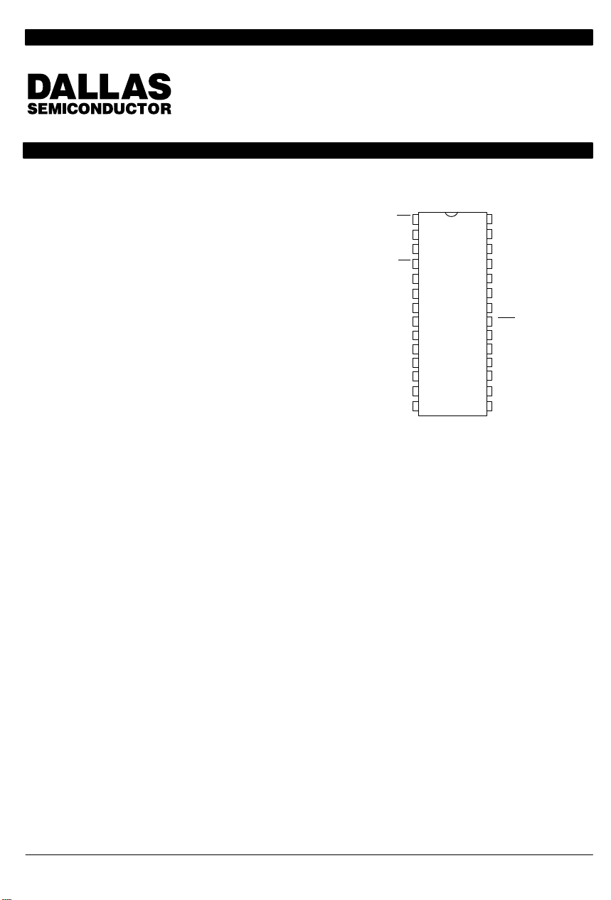
PIN ASSIGNMENT
INT
SDI
SDO
CS
SCLK
NC
RYEL
RLINK
RLCLK
RCLK
RCHCLK
RSER
NC
VSS
1
2
3
4
5
6
7
8
9
10
11
12
13
14 15
28-Pin DIP (600 MIL)
28
27
26
25
24
23
22
21
20
19
18
17
16
VDD
RLOS
RFER
RBV
RCL
RNEG
RPOS
RST
TEST
RSIGSEL
RSIGFR
RABCD
RMSYNC
RFSYNC
The updated DS2182A includes the following changes
from the original DS2182:
• ability to count excessive zeros
• Severely Errored Framing Event indication
• updated AIS detection
• updated RCL detection
• AIS and RCL alarm clear indications
• The DS2182A is upward-compatible from the original
DS2182
DESCRIPTION
The DS2182A T1 Line Monitor Chip is a monolithic
CMOS device designed to monitor real-time performance on T1 lines. The DS2182A frames to the data on
the line, counts errors, and supplies detailed information about the status and condition of the line. Large onboard counters allow the accumulation of errors for ex-
Copyright 1995 by Dallas Semiconductor Corporation.
All Rights Reserved. For important information regarding
patents and other intellectual property rights, please refer to
Dallas Semiconductor data books.
tended periods, which permits a single CPU to monitor a
number of T1 lines. Output clocks that are synchronized
to the incoming data stream are provided for easy extraction of S-Bits, FDL bits, signaling bits, and channel
data. The DS2182A meets the requirements of ANSI
T1.231.
041995 1/22
Page 2
DS2182A
DS2182A BLOCK DIAGRAM Figure 1
CS
SCLK
SDI
INT
SDO
RYEL
RSER
RABCD
RLINK
SERIAL
PORT
INTERFACE
YELLOW
ALARM
DETECT
DATA
DEMUX
INFORMATION REGISTERS
RECEIVE
SYNC
CONTROLLER
BIPOLAR
DECODER
RST
TEST
V
DD
V
SS
RLOS
RCL
RBV
RPOS
RNEG
RLCLK
RSIGFR
RSIGSEL
RCHCLK
RMSYNC
RFSYNC
041995 2/22
RECEIVE
TIMING
RCLK
CRC
SYNCHRONIZER
RFER
Page 3
PIN DESCRIPTION Table 1
PIN SYMBOL TYPE DESCRIPTION
6 NC – No Connect. No internal connection. This pin can be tied to either V
7 RYEL O Receive Yellow Alarm. Transitions high when yellow alarm detected;
8 RLINK O Receive Link Data. Updated with extracted FDL data one RCLK before
9 RLCLK O Receive Link Clock. 4 KHz demand clock for RLINK.
10 RCLK I Receive Clock. 1.544 MHz primary clock.
11 RCHCLK O Receive Channel Clock. 192 KHz clock; identifies time slot (channel)
12 RSER O Receive Serial Data. Received NRZ serial data; updated on rising edges
13 NC - No Connect. No internal connection. This pin can be tied to either V
15 RFSYNC O Receive Frame Sync. Extracted 8 KHz clock, one RCLK wide; F-bit posi-
16 RMSYNC O Receive Multiframe Sync. Extracted multiframe sync; positive-going
17 RABCD O Receive ABCD Signaling. Extracted signaling data output; valid for each
18 RSIGFR O Receive Signaling Frame. High during signaling frames; low during
19 RSIGSEL O Receive Signaling Select. In 193E framing, a .667 KHz clock that identi-
21 RST I Reset. A high-low transition clears all internal registers and resets count-
22
23
RPOS
RNEG
24 RCL O Receive Carrier Loss. High if 192 consecutive 0s appear at RPOS and
25 RBV O Receive Bipolar Violation. High during accused bit time at RSER. If
26 RFER O Receive Frame Error. High during F-bit time when FT or FS errors occur
27 RLOS O Receive Loss of Sync. Indicates sync status; high when internal resync
or VDD, or it can be floated.
goes low when alarm clears.
start of odd frames (193E) and held until next update. Updated with extracted S-bit data one RCLK before start of even frames (193S) and held
until next update.
boundaries.
of RCLK.
or VDD, or it can be floated.
tion in each frame.
edge indicates start of multiframe; 50% duty cycle.
channel in signaling frames. In non-signaling frames, RABCD outputs
the LSB of each channel word.
non-signaling frames (and during resync).
fies signaling frames A and C; a 1.33 KHz clock in 193S.
ers. A high-low-high transition initiates a resync.
I Receive Bipolar Data Inputs. Sampled on falling of RCLK. Tie together
to receive NRZ data and disable bipolar violation monitoring circuitry.
RNEG; goes low upon seeing 12.5% one’s density .
bipolar violation detected, low otherwise.
(193S), or when FPS or CRC errors occur (193E). Low during resync.
is in progress, low otherwise.
DS2182A
SS
SS
041995 3/22
Page 4
DS2182A
PORT PIN DESCRIPTION Table 2
PIN SYMBOL TYPE DESCRIPTION
1 INT O Receive Alarm Interrupt. Flags host controller during alarm conditions.
Active low; open drain output.
2 SDI I Serial Data In. Data for onboard registers. Sampled on rising edge of
SCLK.
3 SDO O Serial Data Out. Control and status information from onboard registers.
Updated on falling edge of SCLK; tri-stated during serial port write or
when CS
is high.
4 CS I Chip Select. Must be low to read or write the serial port.
5 SCLK I Serial Data Clock. Used to read or write the serial port registers.
POWER AND TEST PIN DESCRIPTION Table 3
PIN SYMBOL TYPE DESCRIPTION
14 V
SS
– Signal Ground. 0.0 volts.
20 TEST I T est Mode. Tie to VSS for normal operation.
28 V
DD
– Positive Supply. 5.0 volts.
REGISTER SUMMARY Table 4
REGISTER ADDRESS DESCRIPTION/FUNCTION
BVCR2 0000 Bipolar Violation Count Register 2. LSW of a 16-bit presettable counter
BVCR1 0001 Bipolar Violation Count Register 1. MSW of a 16-bit presettable count-
CRCCR 0010 CRC Error Count Register. 8-bit presettable counter that records CRC6
OOFCR 0011 OOF Count Register. 8-bit presettable counter that records OOF events.
FECR 0100 Frame Error Count Register. 8-bit presettable counter that records indi-
RSR1 0101 Receive Status Register 1. Reports alarm conditions.
RIMR1 0110 Receive Interrupt Mask Register 1. Allows masking of individual alarm-
RSR2 0111 Receive Status Register 2. Reports alarm conditions.
RIMR2 1000 Receive Interrupt Mask Register 2. Allows masking of individual alarm-
RCR1 1001 Receive Control Register 1. Programs device operating characteristics.
RCR2 1010 Receive Control Register 2. Programs device operating characteristics.
that records individual bipolar violations.
er that records individual bipolar violations.
errored words in the 193E frame mode.
OOF events are defined by RCR1.5 and RCR1.6.
vidual bit errors in the framing pattern.
generated interrupts from RSR1.
generated interrupts from RSR2.
041995 4/22
Page 5
DS2182A
SERIAL PORT INTERFACE
The port pins of the DS2182A serve as a microprocessor/microcontroller-compatible serial port. Eleven onboard registers allow the user to update operational
characteristics and monitor device status via a host controller, minimizing hardware interfaces. The port on the
DS2182A can be read from or written to at any time. Serial port reads and writes are independent of T1 line timing signals RCLK, RPOS, and RNEG. However, RCLK
is needed in order to clear RSR1 and RSR2 after reads.
ADDRESS/COMMAND
Reading or writing the control, configuration or status
registers requires writing one address/command byte
prior to transferring register data. The first bit written
(LSB) of the address/command word specifies register
read or write. The following four bits identify the register
address. The next two bits are reserved and must be set
to 0 for proper operation. The last bit of the address/
command word enables burst mode when set; the burst
mode causes all registers to be consecutively read or
written to. Data is read and written to the DS2182A LSB
first.
CHIP SELECT AND CLOCK CONTROL
All data transfers are initiated by driving the CS input
low. Input data is latched on the rising edge of SCLK and
must be valid during the previous low period of SCLK to
prevent momentary corruption of register data during
writes. Data is output on the falling edge of SCLK and
held to the next falling edge. All data transfers are terminated if the CS
is disabled and SDO is tri-stated when CS is high.
input transitions high. Port control logic
DATA I/O
Following the eight SCLK cycles that input an address/
command byte to write, a data byte is strobed into the
addressed register on the rising edge of the next eight
SCLK cycles. Following an address/command word to
read, contents of the selected register are output on the
falling edges of the next eight SCLK cycles. The SDO
pin is tri-stated during device write and can be tied to
SDI in applications where the host processor has a bidirectional I/O pin.
BURST MODE
The burst mode allows all onboard registers to be consecutively written to or read by the host processor. A
burst read is used to poll all registers; RSR1 and RSR2
contents will be unaffected. This feature minimizes device initialization time on system power-up or reset.
Burst mode is initiated when ACB.7 is set and the address is 0000. A burst is terminated by a low-high transition on CS
.
ACB: ADDRESS COMMAND BYTE Figure 2
(MSB) (LSB)
BM
SYMBOL POSITION NAME AND DESCRIPTION
BM ACB.7 Burst Mode. If set (and register address is 0000) burst read or write is en-
- ACB.6 Reserved, must be 0 for proper operation.
- ACB.5 Reserved, must be 0 for proper operation.
ADD3 ACB.4 MSB of register address.
ADD0 ACB.1 LSB of register address.
R/W ACB.0 Read/Write Select.
– – ADD3 ADD2 ADD1 ADD0 R/W
abled.
0 = write addressed register
1 = read addressed register
041995 5/22
Page 6
DS2182A
SERIAL PORT READ/WRITE Figure 3
CS
SCLK
SDI
SDO
R/W A0 A1 A2 A3 0 0 BM D0 D1 D2 D3 D4 D5 D6 D7
ADDRESS/COMMAND DATA INPUT/OUTPUT
NOTES:
1. SDI is sampled on rising edge of SCLK.
2. SDO is updated on falling edge of SCLK.
OPERATION OF THE COUNTERS
All four of the counters in the DS2182A can be preset by
the user to establish an event count interrupt threshold.
The counters count up from the preset value until they
reach saturation. At saturation, each additional event
reading all of the registers or only the counters. If
RCR1.4 is set, then any read of the registers, burst
mode or not, will clear the count in all four counters. If the
user wishes to read the port and not clear the counters,
then RCR1.4 must be cleared first.
occurrence sets the appropriate bit in RSR2 and generates an interrupt if enabled by RIMR2.
The counter registers can be read or written to at any
time with the serial port, which operates totally asynchThe DS2182A contains an auto counter reset feature in
the burst read mode. If RCR1.4 is set, then the user can
burst read the four counters (five registers), and all four
counters will be automatically reset to 0 after the read
takes place. Since the burst mode can be terminated at
any time by taking CS
high, the user has the option of
ronously with the monitoring of the T1 line. Reading a
register will not affect the count as long as RCR1.4 is
cleared. The dual buffer architecture of the DS2182A in-
sures that no error events will be missed while the serial
port is being accessed for reads.
BVCR1: BIPOLAR VIOLATION COUNT REGISTER 1;
BVCR2: BIPOLAR VIOLATION COUNT REGISTER 2 Figure 4
(MSB) (LSB)
BV7 BV6 BV5 BV4 BV3 BV2 BV1 BV0
SYMBOL POSITION NAME AND DESCRIPTION
BV7 BVCR.7 MSB of bipolar violation count
BV0 BVCR.0 LSB of bipolar violation count
Bipolar Violation Count Register 1 (BVCR1) is the most
significant word and BVCR2 is the least significant word
of a presettable 16-bit counter that records individual bipolar violations. If the B8ZS mode is enabled (RCR2.2 =
1), then B8ZS code words are not counted. The BVCR
can also be programmed to count excessive zeros by
count occurrences of 8 consecutive zeros when B8ZS is
enabled or 16 consecutive zeros when B8Z5 is dis-
abled. This counter increments at all times and is not
disabled by a loss of sync condition (RLOS = 1). The
counter saturates at 65,535 and generates an interrupt
for each occurrence after saturation if RIMR2.0 is set.
setting the RCR2.5 bit. In this mode, the BVCR will
NOTE:
1. In order to properly preset the Bipolar Violation Count Register, BVCR2 must be written to before BVCR1 is
written to.
041995 6/22
Page 7

CRCCR: CRC COUNT REGISTER Figure 5
(MSB) (LSB)
CRC7 CRC6 CRC5 CRC4 CRC3 CRC2 CRC1 CRC0
SYMBOL POSITION NAME AND DESCRIPTION
CRC7 CRCCR.7 MSB of CRC6 word error count
CRC0 CRCCR.0 LSB of CRC6 word error count
DS2182A
The CRC Count Register (CRCCR) is an 8-bit presettable counter that records word errors in the Cyclic Redundancy Check (CRC). This 8-bit binary counter saturates at 255 and generates an interrupt for each
in this register is only valid in the 193E framing mode
(RCR2.4 = 1) and is reset and disabled in the 193S framing mode (RCR2.4 = 0). The count is disabled during a
loss of sync condition (RLOS = 1).
occurrence after saturation if RIMR2.1 is set. The count
OOFCR: OOF COUNT REGISTER Figure 6
(MSB) (LSB)
OOF7
OOF6 OOF5 OOF4 OOF3 OOF2 OOF1 OOF0
SYMBOL POSITION NAME AND DESCRIPTION
OOF7 OOFCR.7 MSB of OOF event count
OOF0 OOFCR.0 LSB of OOF event count
The OOF Count Register (OOFCR) is an 8-bit presettable counter that records Out Of Frame (OOF) events.
OOF events are defined by RCR1.5 and RCR1.6. This
rupt for each occurrence after saturation if RIMR2.2 is
set. The count is disabled during a loss of sync condition (RLOS = 1).
8-bit counter saturates at 255 and generates an inter-
FECR: FRAME ERROR COUNT REGISTER Figure 7
(MSB) (LSB)
FE7
SYMBOL POSITION NAME AND DESCRIPTION
FE7 FECR.7 MSB of frame error count
FE0 FECR.0 LSB of frame error count
FE6 FE5 FE4 FE3 FE2 FE1 FE0
The Frame Error Count Register (FECR) is an 8-bit presettable counter that records individual frame bit errors.
In the 193E mode (RCR2.4 = 1), the FECR records bit
errors in the FPS framing pattern (001011). In the 193S
mode (RCR2.4 = 0), the FECR records bit errors in both
the FT (101010) and FS (001110) framing patterns if
RCR1.3 is set. If RCR1.3 is cleared, then the FECR only
records bit errors in the FT pattern. This 8-bit counter
saturates at 255 and generates an interrupt for each occurrence after saturation if RIMR2.3 is set. The count is
disabled during a loss of sync condition (RLOS = 1).
041995 7/22
Page 8

DS2182A
RSR1: RECEIVE STATUS REGISTER 1 Figure 8
(MSB) (LSB)
8ZD 16ZD RCL RYEL RLOS B8ZSD RBL COFA
SYMBOL POSITION NAME AND DESCRIPTION
8ZD RSR1.7 8 Zero Detect. Set when a string of eight consecutive 0s has been re-
16ZD RSR1.6 16 Zero Detect. Set when a string of 16 consecutive 0s has been received
RCL RSR1.5 Receive Carrier Loss. Set when a string of 192 consecutive 0s has been
RYEL RSR1.4 Receive Y ellow Alarm. Set when yellow alarm is detected. The format of
RLOS RSR1.3 Receive Loss of Sync. Set when resync is in progress.
B8ZSD RSR1.2 B8ZS Code Word Detect. Set when a B8ZS code word is received at
RBL RSR1.1 Receive Blue Alarm. Set when over a 3 ms window, 5 or less zeros are
COFA RSR1.0 Change of Frame Alignment. Set when the last resync resulted in a
ceived at RPOS and RNEG.
at RPOS and RNEG.
received at RPOS and RNEG. Cleared when 14 or more ones out of 112
possible bit positions are received.
yellow alarm is determined by RCR2.3 and RCR2.4.
RPOS and RNEG independent of whether the B8ZS mode is enabled or
not (RCR2.2).
received. Cleared when over a 3 ms window, 6 or more zeros are received.
change of frame or multiframe alignment.
NOTE:
1. Alarms 8ZD and 16ZD are cleared on the next occurrence of a 1 at RPOS and RNEG.
RECEIVE STATUS REGISTERS
The receive status registers (RSR1 and RSR2) can be
used in either a polled or an interrupt configuration. In a
polled configuration, the user reads the RSR at regular
intervals to check for alarms. In an interrupt configuration, the user monitors the INT pin. When the INT pin
goes low, an alarm condition has occurred and has been
reported in one of the RSRs. The processor can then
read the RSRs to find which bits have been set. All of the
bits in the RSRs operate in a latched fashion. That is,
once set, they remain set until read. The bits in the RSR
are cleared when read unless the read was performed in
the burst mode or the alarm condition still exists.
YELLOW ALARM
193S BIT 2. If RCR2.4 = 0 and RCR2.3 = 0, then the
DS2182A examines bit 2 of all incoming channels for
041995 8/22
the presence of a yellow alarm. If bit 2 is set to 0 in 256
consecutive channels, then the reception of a yellow
alarm is declared. The alarm is considered cleared
when the first channel with bit 2 set to a 1 is received.
193S S-BIT. If RCR2.4 = 0 and RCR2.3 = 1, then the
DS2182A examines the S-bit position of frame 12 for the
presence of a yellow alarm. The DS2182A declares the
presence of a yellow alarm on the first occurrence of the
S-bit in frame 12 being set to 1. The alarm is considered
cleared when this S-bit returns to 0.
193E FDL. If RCR2.4 = 1, then the DS2182A examines
the FDL for a repeating 00FF pattern. If this pattern is
received in the FDL 16 consecutive times without error,
then a yellow alarm is declared. The alarm is consid-
ered cleared as soon as any pattern other than 00FF is
received.
Page 9

RIMR1: RECEIVE INTERRUPT MASK REGISTER 1 Figure 9
(MSB) (LSB)
8ZD 16ZD RCL RYEL RLOS B8ZSD RBL COFA
SYMBOL POSITION NAME AND DESCRIPTION
8ZD RIMR1.7 8 Zero Detect Mask.
1 = interrupt enabled
0 = interrupt masked
16ZD RIMR1.6 16 Zero Detect Mask.
1 = interrupt enabled
0 = interrupt masked
RCL RIMR1.5 Receive Carrier Loss Mask.
1 = interrupt enabled
0 = interrupt masked
RYEL RIMR1.4 Receive Yellow Alarm Mask.
1 = interrupt enabled
0 = interrupt masked
RLOS RIMR1.3 Receive Loss Of Sync Mask.
1 = interrupt enabled
0 = interrupt masked
B8ZSD RIMR1.2 B8ZS Code Word Detect Mask.
1 = interrupt enabled
0 = interrupt masked
RBL RIMR1.1 Receive Blue Alarm Mask.
1 = interrupt enabled
0 = interrupt masked
COFA RIMR1.0 Change Of Frame Alignment Mask.
1 = interrupt enabled
0 = interrupt masked
DS2182A
041995 9/22
Page 10

DS2182A
RSR2: RECEIVE STATUS REGISTER 2 Figure 10
(MSB) (LSB)
SEFE
SYMBOL POSITION NAME AND DESCRIPTION
SEFE RSR2.7 Severely Errored Framing Event. Set when 2 out of 6 framing bits (Ft or
RCLC RSR2.6 Receive Carrier Loss Clear. Set when the carrier signal is restored; will
RBLC RSR2.5 Receive Blue Alarm Clear. Set when the Blue Alarm (AIS) is no longer de-
FERR RSR2.4 Frame Bit Error. Set when FT (193S) or FPS (193E) bit errors occur.
FECS RSR2.3 Frame Error Count Saturation. Set on the next frame error event after
OOFCS RSR2.2 Out Of Frame Count Saturation. Set on the next OOF event after the
CRCCS RSR2.1 CRC Count Saturation. Set on the next CRC error event after the 8-bit
BPVCS RSR2.0 Bipolar Violation Count Saturation. Set on the next BPV error event af-
RCLC RBLC FERR FECS OOFCS CRCCS BPVCS
FPS) are received in error.
remain set until read.
tected; will remain set until read.
the 8-bit Frame Error Count Register (FECR) saturates at 255.
8-bit OOF Count Register (OOFCR) saturates at 255.
CRC Count Register (CRCCR) saturates at 255.
ter the 16-bit Bipolar Violation Count Register (BVCR) saturates at 65,535.
RIMR2: RECEIVE INTERRUPT MASK REGISTER 2 Figure 11
(MSB) (LSB)
SEFE
SYMBOL POSITION NAME AND DESCRIPTION
SEFE RIMR2.7 Severely Errored Framing Event Mask.
RCLC RIMR2.6 Receive Carrier Loss Clear Mask.
RBLC RIMR2.5 Receive Blue Alarm Clear Mask.
FERR RIMR2.4 Frame Bit Error Mask.
FECS RIMR2.3 Frame Error Count Saturation Mask.
OOFCS RIMR2.2 Out Of Frame Count Saturation Mask.
RCLC RBLC FERR FECS OOFCS CRCCS BPVCS
0 = interrupt masked
1 = interrupt enabled
0 = interrupt masked
1 = interrupt enabled
0 = interrupt masked
1 = interrupt enabled
1 = interrupt enabled
0 = interrupt masked
1 = interrupt enabled
0 = interrupt masked
1 = interrupt enabled
0 = interrupt masked
041995 10/22
Page 11

DS2182A
CRCCS RIMR2.1 CRC Count Saturation Mask.
1 = interrupt enabled
0 = interrupt masked
BPVCS RIMR2.0 Bipolar Violation Count Saturation Mask.
1 = interrupt enabled
0 = interrupt masked
RCR1: RECEIVE CONTROL REGISTER 1 Figure 12
(MSB) (LSB)
ARC OOF1 OOF2 ACR SYNCC SYNCT SYNCE RESYNC
SYMBOL POSITION NAME AND DESCRIPTION
ARC RCR1.7 Auto Resync Criteria.
OOF1 RCR1.6 Out Of Frame 1. OOF event description. Valid when RCR1.5 is cleared
OOF2 RCR1.5 Out Of Frame 2. OOF event description.
ACR RCR1.4 Auto Counter Reset. When set, all four of the counters will be reset to 0
SYNCC RCR1.3 Sync Criteria. Determines the type of algorithm utilized by the receive syn-
SYNCT RCR1.2 Sync Time.
SYNCE RCR1.1 Sync Enable. If clear, the DS2182A automatically begins a resync if the
RESYNC RCR1.0 Resync. When toggled low to high, the DS2182A initiates a resync imme-
SYNCHRONIZER
The heart of the monitor is the receive synchronizer.
This circuit serves two purposes: 1) monitors the incoming data stream for loss of frame or multiframe alignment, and 2) searches for new frame alignment pattern
when sync loss is detected. When sync loss is detected, the synchronizer begins an off-line search for the
new alignment; all output timing signals remain at the
old alignment with the exception of RSIGFR, which is
1 = resync on OOF event only
0 = resync on OOF event or Receive Carrier Loss (RCL)
1 = 2 out of 5 frame bits (FT or FPS) in error
0 = 2 out of 4 frame bits (FT or FPS) in error
1 = 2 out of 6 frame bits (FT or FPS) in error
0 = follow OOF event described in RCR1.6
when read.
chronizer; differs for each frame mode.
193S Framing (RCR2.4 = 0)
0 = synchronize to frame boundaries using FT pattern, then search for multiframe by using FS.
1 = cross couple FT and FS patterns in sync algorithm.
193E Framing (RCR2.4 = 1)
0 = normal sync (utilizes FPS only).
1 = validate new alignment with CRC before declaring sync.
1 = validate 24 consecutive F-bits before declaring sync.
0 = validate 10 consecutive F-bits before declaring sync.
conditions described in RCR1.7 are met. If set, no auto resync occurs.
diately . The bit must be cleared and set again for subsequent resyncs.
forced low during resync. When one and only one candidate is qualified, the output timing moves to the new
alignment at the beginning of the next multiframe. One
frame later, RLOS will transition low, indicating valid
sync and the resumption of the normal sync monitoring
mode. Several bits in the RCR1 allow tailoring of the resync algorithm by the user. These bits are described below.
041995 11/22
Page 12

DS2182A
FRAME
SYNC CRITERIA (RCR1.3)
193E. Bit RCR1.3 determines which sync algorithm is
utilized when resync is in progress (RLOS = 1). In 193E
framing, when RCR1.3 = 0, the synchronizer will lock
only to the FPS pattern and will move to the new frame
and multiframe alignment after the framing candidate is
qualified. RLOS will go low one frame after the move to
the new alignment. When RCR1.3 = 1, the new alignment is further tested by a CRC6 code match. RLOS will
transition low after a CRC6 match occurs. If no CRC6
match occurs in three attempts (three multiframes), the
algorithm resets and a new search for the FPS pattern
begins. It takes 9 ms for the synchronizer to check the
first CRC6 code after the new FPS alignment has been
loaded. Each additional CRC6 test takes 3 ms. Regardless of the state of RCR1.3, if more than one candidate
exists after 24 ms, the synchronizer begins eliminating
emulators by testing their CRC6 codes in order to find
the true framing candidate.
193S. In 193S framing, when RCR1.3 = 1, the synchronizer cross-checks the FT pattern with the FS pattern to
help eliminate false framing candidates such as digital
milliwatts. The FS patterns are compared to the repeating pattern ...00111000111000...(00111x0 if RCR2.3 =
1). In this mode, FT and FS must be correctly identified
AVERAGE REFRAME TIME Table 5
FRAME
MODE
193S 3.0ms 3.75ms 4.5ms 6.5ms 7.25ms 8.0ms
193E 6.0ms 7.5ms 9.0ms 13.0ms 14.5ms 16.0ms
MIN. AVG. MAX. MIN. AVG. MAX.
RCR1.2 = 0 RCR1.2 = 1
by the synchronizer before sync is declared. Clearing
RCR1.3 causes the synchronizer to search for the FT
pattern (101010...) without cross-coupling the FS pat-
tern. Frame sync is established using the FT informa-
tion, while multiframe sync is established only if valid FS
information is present. If no valid FS pattern is identified,
the synchronizer moves to the FT alignment, RLOS
goes low, and a false multiframe position may be indi-
cated by RMSYNC. RFER indicates when the received
S-bit pattern does not match the assumed internal multi-
frame alignment. This mode will be used in applications
where non-standard S-bit patterns exist. In such appli-
cations, multiframe alignment information can be de-
coded externally by using the S-bits present at RLINK.
SYNC TIME (RCR1.2)
Bit RCR1.2 determines the number of consecutive
framing pattern bits to be qualified before SYNC is de-
clared. If RCR1.2 =1, the algorithm validates 24 bits; if
RCR1.2 = 0, 10 bits are validated. Validating 24 bits re-
sults in superior false framing protection while 10-bit
testing minimizes reframe time. In either case, the syn-
chronizer only establishes resync when one and only
one candidate is found (see Table 5).
NOTE:
1. Average reframe time is defined here as the average time it takes from the start of resync (rising edge of
RLOS) to the actual loading of the new alignment (on a multiframe edge) into the output receive timing.
SYNC ENABLE (RCR1.1)
When RCR1.1 is cleared, the receiver initiates automatic resync if an OOF event occurs or if carrier loss (192
consecutive 0s) occurs (depends on RCR1.7). When
RCR1.1 is set, the automatic resync circuitry is disabled. In this case, resync can only be initiated by setting RCR1.0 to 1 or externally transitioning RST
low to high. Note that using RST to initiate a resync resets the output timing while RST
041995 12/22
is low; use of RCR1.1
from
will not affect the output timing until the new alignment is
located.
RESYNC (RCR1.0)
A 0-to-1 transition of RCR1.0 causes the synchronizer
to search for the framing pattern sequence immediately,
regardless of the internal sync status. In order to initiate
another resync command, this bit must be cleared and
then set again.
Page 13

RCR2: RECEIVE CONTROL REGISTER 2 Figure 13
(MSB) (LSB)
– – BVCRF FM SFYEL B8ZS – –
SYMBOL POSITION NAME AND DESCRIPTION
- RCR2.7 Reserved; must be 0 for proper operation.
- RCR2.6 Reserved; must be 0 for proper operation.
BVCRF RCR2.5 Bipolar Violation Count Register Function Select.
0 = do not count excessive zeros
1 = count excessive zeros
FM RCR2.4 Frame Mode.
1 = Extended Superframe (193E, 24 frames per Superframe).
0 = Superframe (193S or D4, 12 frames per Superframe).
SFYEL RCR2.3 SF Yellow Mode Select.
1 = 1 in the S-bit position of frame 12.
0 = 0 in bit 2 of all channels.
B8ZS RCR2.2 Bipolar Eight Zero Substitution.
1 = B8ZS enabled.
0 = B8ZS disabled.
- RCR2.1 Reserved; must be 0 for proper operation.
- RCR2.0 Reserved; must be 0 for proper operation.
DS2182A
193S RECEIVE MULTIFRAME TIMING Figure 14
FRAME#
RFSYNC
RMSYNC
RSIGSEL
RSIGFR
RLCLK
RABCD
RLINK
12345678910111212345
BABA
NOTES:
1. Signaling data is updated during signaling frames on channel boundaries. Pin RABCD is the LSB of each
channel word in non-signaling frames.
2. RLINK data (S-bit) is updated one bit-time prior to S-bit frames and held for two frames.
041995 13/22
Page 14

DS2182A
193E RECEIVE MULTIFRAME TIMING Figure 15
FRAME#
RFSYNC
RMSYNC
RSIGSEL
RSIGFR
RLCLK
RABCD
RLINK
1 2 3 4 5 6 7 8 9 10 11 12 13 14 15 16 17
DA CBD
18 19 20 21 22 23 24
NOTES:
1. Signaling data is updated during signaling frames on channel boundaries. Pin RABCD is the LSB of each
channel word in non-signaling frames.
2. RLINK data (FDL data) is updated one bit-time prior to odd frames and held for two frames.
041995 14/22
Page 15

RECEIVE MULTIFRAME BOUNDARY TIMING Figure 16
RCLK
RPOS,
RNEG
RFSYNC
RMSYNC
RSIGSEL
RSIGFR
RLCLK
RCHCLK
LSB MSBF
CHANNEL 1
LSB MSB LSB MSB
DS2182A
CHANNEL 2
RLINK
RABCD
CHANNEL 23 CHANNEL 24 CHANNEL 1
RSER
LSB MSB LSB MSBF
NOTES:
1. RLINK timing is shown for 193E; in 193S, RLINK is updated on even frame boundaries and is held across
multiframe edges.
2. Total delay from RPOS and RNEG to RSER output is 13 RCLK periods.
ALARM OUTPUTS
The transceiver also provides direct alarm outputs for
applications when additional decoding and demuxing
are required to supplement the onboard alarm logic.
RLOS OUTPUT
The receive loss of sync output indicates the status of
the receiver synchronizer circuitry; when high, an offline resynchronization is in progress and a high-low
transition indicates that resync is complete. The RLOS
bit (RSR1.3) is a latched version of the RLOS output. If
the auto-resync mode is selected (RCR1.1 = 0), RLOS
is a real-time indication of a carrier loss or OOF event
occurrence.
RYEL OUTPUT
The yellow alarm output transitions high when a yellow
alarm is detected. A high-low transition indicates the
alarm condition has been cleared. The RYEL bit
(RSR1.4) is a latched version of the RYEL output.
041995 15/22
Page 16

DS2182A
RBV OUTPUT
The bipolar violation output transitions high when the
accused bit emerges at RSER. RBV goes low at the
next bit time if no additional violations are detected.
RFER OUTPUT
The receive frame error output transitions high at the Fbit time and is held high for two bit periods when a frame
bit error occurs. In 193S, framing FT and FS patterns
are tested. The FPS pattern is tested in 193E framing.
Additionally , in 193E framing, RFER reports CRC6 code
word errors by a low-high-low transition (one bit period-
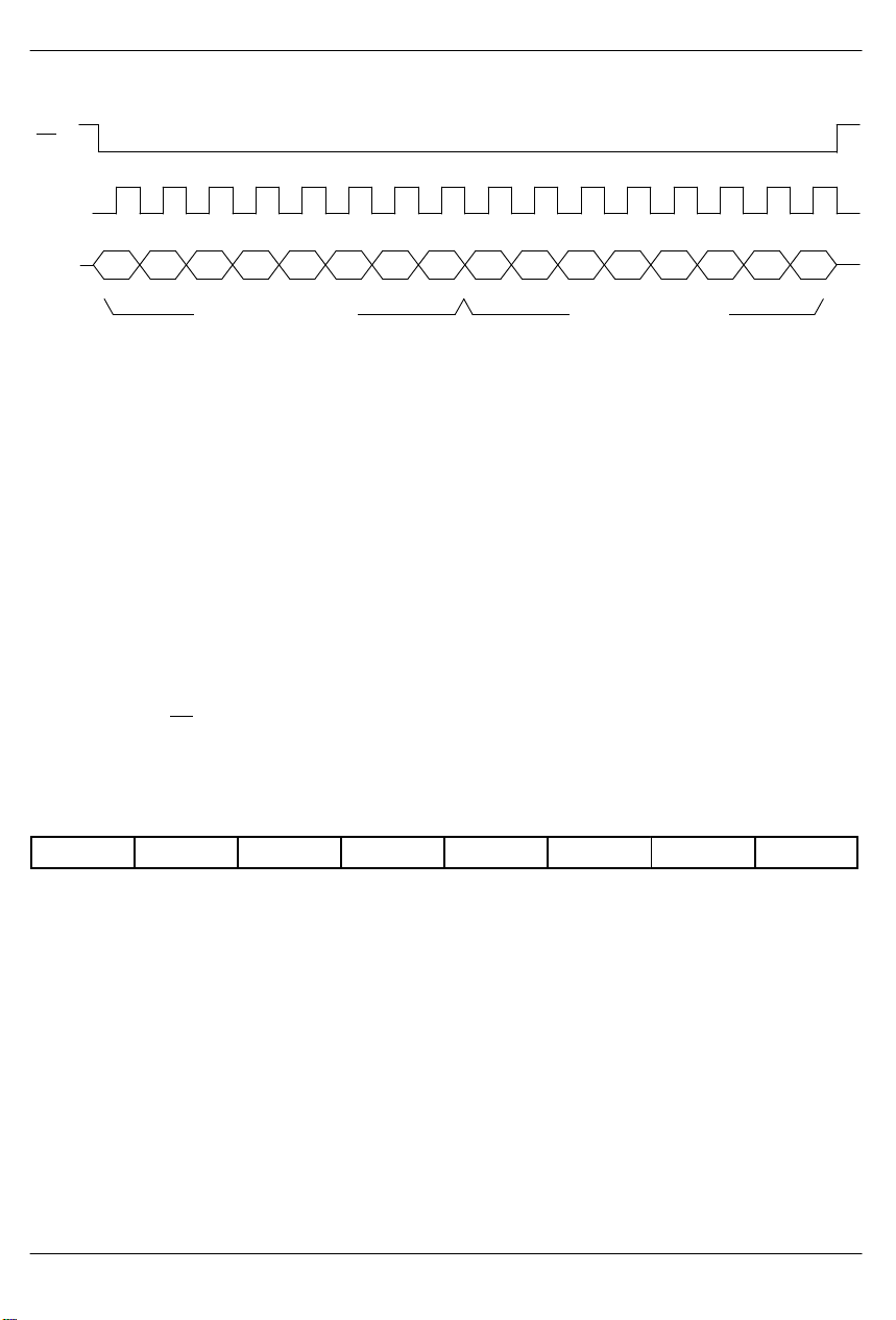
ALARM OUTPUT TIMING Figure 17
RCLK
RFSYNC
RMSYNC
RFER
RBV
wide) one-half RCLK period before a low-high transition
on RMSYNC (see Figure 17).
RESET
A high-low transition on RST clears all registers and
forces an immediate resync when RST returns high.
RST must be held low on system power-up to insure
proper initialization of the counters and registers. Following reset, the host processor should restore all control modes by writing appropriate registers with control
data.
RCL
RLOS
NOTES:
1. RFER transitions high during F-bit time if received framing pattern bit is in error. (Frame 12 F-bits in 193S are
ignored if RCR2.3 = 1.) Also, in 193E, RFER transitions high 1/2 bit-time before rising edge of RMSYNC to
indicate a CRC6 error for the previous multiframe.
2. RBV indicates received bipolar violation and transitions high when accused bit emerges from RSER. If B8ZS
is enabled, RBV will not report the zero replacement code.
3. RCL transitions high when 192 consecutive bits are 0; RCL transitions low upon reception of 12.5% ones
density.
4. RLOS transitions high during F-bit time that caused an OOF event if auto-resync is enabled (RCR1.1 = 0).
Resync also occurs when loss of carrier is detected (RCL = 1) if RCR1.7 = 0. When RCR1.1 = 1, RLOS remains low until resync occurs, regardless of OOF or carrier loss flags. In this situation, resync is initiated
only when RCR1.0 transitions low-to-high or the RST
041995 16/22
pin transitions high-low-high.
Page 17

DS2182A
ABSOLUTE MAXIMUM RATINGS*
Voltage on Any Pin Relative to Ground -1.0V to 7.0V
Operating Temperature 0°C to +70°C
Storage Temperature -55°C to 125°C
Soldering Temperature 260°C for 10 seconds
* This is a stress rating only and functional operation of the device at these or any other conditions above
those indicated in the operation sections of this specification is not implied. Exposure to absolute maximum rating conditions for extended periods of time may affect reliability.
RECOMMENDED DC OPERATING CONDITIONS (0°C to +70°C)
PARAMETER SYMBOL MIN TYP MAX UNITS NOTES
Logic 1 V
Logic 0 V
Supply V
IH
IL
DD
2.0
-0.3
4.5
VDD+.3 V
+0.8 V
5.5 V
DC ELECTRICAL CHARACTERISTICS (0°C to 70°C; VDD=5V + 10%)
PARAMETER SYMBOL MIN TYP MAX UNITS NOTES
Supply Current I
Input Leakage I
Output Current @ 2.4V I
Output Current @ 0.4V I
Output Leakage I
DD
IL
OH
OL
LO
-1.0 +1.0 µA 3
-1.0 mA 4
+4.0 mA 5
-1.0 +1.0 µA 6
3 mA 1,2
CAPACITANCE (tA = 25°C)
PARAMETER SYMBOL MIN TYP MAX UNITS NOTES
Input Capacitance C
Output Capacitance C
IN
OUT
5 pF
7 pF
NOTES:
1. RCLK = 1.544 MHz.
2. Outputs open.
3. 0V < V
4. All outputs except INT
5. All outputs.
6. Applies to SDO when tri-stated.
< VDD.
IN
which is open collector.
041995 17/22
Page 18

DS2182A
CHARACTERISTICS
1,2
SERIAL PORT (0°C to 70°C; VDD = 5V + 10%)
PARAMETER SYMBOL MIN TYP MAX UNITS NOTES
SDI to SCLK Setup t
SCLK to SDI Hold t
CDH
SDI to SCLK Falling Edge t
SCLK Low Time t
SCLK High Time t
SCLK Rise and Fall Times tR,t
CS to SCLK Setup t
SCLK to CS hold t
CS Inactive Time t
SCLK to SDO Valid t
CS to SDO High Z t
CCH
CWH
CDV
CDZ
DC
CD
CL
CH
F
CC
50 ns
50 ns
50 ns
250 ns
250 ns
100 ns
50 ns
50 ns
2.5 µs
200 ns
75 ns
NOTES:
1. Measured at VIH = 2.0 or VIL = .8 and 10ns maximum rise and fall time.
2. Output load capacitance = 100 pF.
AC ELECTRICAL CHARACTERISTICS
1,2
RECEIVE (0°C to 70°C; VDD = 5V + 10%)
PARAMETER SYMBOL MIN TYP MAX UNITS NOTES
Propagation Delay RCLK to
RMSYNC, RFSYNC, RSISEL,
t
PRS
75 ns
RSIGFR, RLCLK, RCHCLK
Propagation Delay RCLK to
RSER, RABCD, RLINK
Transition Time All Outputs t
RCLK Period t
RCLK Pulse Width tWL,t
RCLK Rise and Fall Times tR,t
RPOS, RNEG Setup to RCLK
Falling
RPOS, RNEG Hold to RCLK
Falling
Propagation Delay RCLK to
RLOS, RYEL, RBV, RCL, RFER
Minimum RST Pulse Width t
t
PRD
TTR
t
SRD
t
HRD
t
PRA
RST
75 ns
20 ns
P
WH
F
648 ns
324 ns
20 ns
50 ns
50 ns
75 ns
1 µs
NOTES:
1. Measured at VIH = 2.0 or VIL = .8 and 10ns maximum rise and fall time.
2. Output load capacitance = 100 pF.
041995 18/22
Page 19

SERIAL PORT WRITE AC TIMING DIAGRAM Figure 18
t
CC
CS
t
SCC
t
CH
t
t
F
R
t
CCH
SCLK
SDI
t
t
DC
t
CDH
CL
LSB
t
CD
LSB
t
CDH
1
MSB
CONTROL BYTE DATA BYTE
NOTES:
1. Data byte bits must be valid across low clock periods to prevent transients in operating modes.
2. Shaded regions indicate don’t-care states of input.
SERIAL PORT READ1 AC TIMING DIAGRAM Figure 19
DS2182A
t
CWH
CS
SCLK
t
CDV
SDO
NOTE:
1. Serial port write must precede a port read to provide address information.
t
CDZ
High Z
041995 19/22
Page 20

DS2182A
RECEIVE AC TIMING DIAGRAM Figure 20
RCLK
t
PRD
RSER, RABCD,
RLINK
t
t
RST
t
PRS
PRA
RMSYNC, RFSYNC
RSIGSEL, RSIGFR
RLCLK, RCHCLK
RYEL, RCL, RBV
RFER, RLOS
RST
t
P
t
WL
t
WH
t
F
t
R
RPOS, RNEG
t
SRDtHRD
041995 20/22
Page 21

DS2182A T1 LINE MONITOR 28-PIN DIP
28 15
DS2182A
B
1
13 EQUAL SPACES AT + .010
INCHES
DIM MIN MAX
A 1.445 1.470
B 0.530 0.550
C 0.140 0.160
D 0.600 0.625
E 0.015 0.040
F 0.120 0.145
G 0.090 0.110
H 0.600 0.680
J 0.008 0.012
K 0.015 0.022
A
TNA
14
D
C
E
GK
F
J
H
041995 21/22
Page 22

DS2182A
DS2182AQ T1 LINE MONITOR 28-PIN PLCC
E
E1
N
1
CH1
E2
INCHES
DIM MIN MAX
A 0.165 0.180
A1 0.090 0.120
A2 0.020 -
B 0.026 0.033
B1 0.013 0.021
C 0.009 0.012
D 0.485 0.495
D1 0.450 0.456
D2 0.390 0.430
E 0.485 0.495
E1 0.450 0.456
E2 0.390 0.430
L1 0.060 -
N 28 e1 0.050 BSC
CH1 0.042 0.048
D1 D D2
e1
B
L1
B1
A
C
A1A2
041995 22/22
 Loading...