

Page 1
DS2181A
DS2181A
CEPT Primary Rate Transceiver
FEATURES
• Single–chip primary rate transceiver meets CCITT
standards G.704, G.706 and G.732
• Supports new CRC4-based framing standards and
CAS and CCS signalling standards
• Simple serial interface used for device configuration
and control in processor mode
• Hardware mode requires no host processor;
intended for stand-alone applications
• Comprehensive, on-chip alarm generation, alarm
detection, and error logging logic
• Shares footprint with DS2180A T1 Transceiver
• Companion to DS2175 T1/CEPT Elastic Store,
DS2186 Transmit Line Interface, DS2187 Receive
Line Interface, and DS2188 Jitter Attenuator
• 5V supply; low-power CMOS technology
DESCRIPTION
The DS2181A is designed for use in CEPT networks
and supports all logical requirements of CCITT Red
Book Recommendations G.704, G.706 and G.732. The
transmit side generates framing patterns and CRC4
codes, formats outgoing channel and signalling data,
and produces network alarm codes when enabled. The
receive side decodes the incoming data and establishes frame, CAS multiframe, and CRC4 multiframe
alignments. Once synchronized, the device extracts
channel, signalling, and alarm data.
A serial port allows access to 14 on-chip control and status registers in the processor mode. In this mode, a host
processor controls features such as error logging, perchannel code manipulation, and alteration of the receive
synchronizer algorithm.
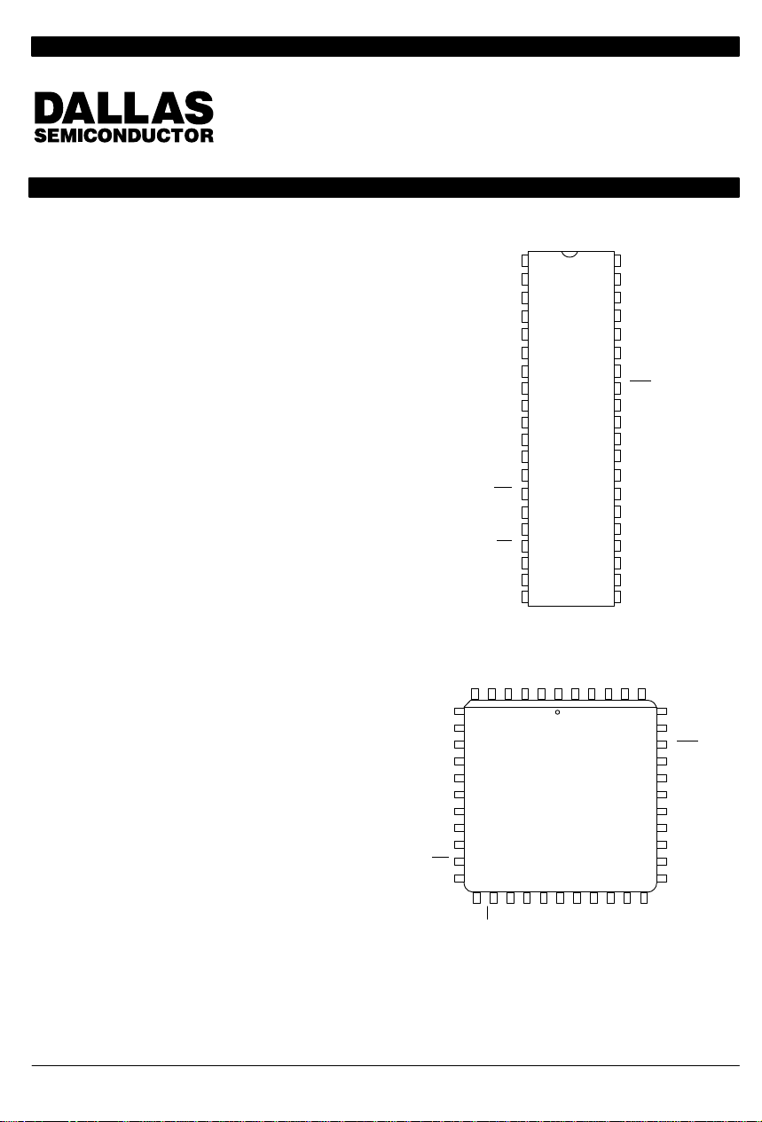
PIN ASSIGNMENT
TMSYNC
TFSYNC
TCLK
TCHCLK
TSER
TMO
TXD
TSTS
TSD
TIND
TAF
TPOS
TNEG
INT
SDI
SDO
CS
SCLK
SPS
VSS
40-Pin DIP (600 MIL)
RFSA
TCHCLK
TCLK
6543214443424140
TSER
7
TMO
8
TXD
9
TSTS
10
11
TSD
12
TIND
TAF
TPOS
TNEG
INT
SDI
13
14
15
16
17
44-PIN PLCC
18 19 20 21 22 23 24 25 26 27 28
CS
SDO
SCLK
1
2
3
4
5
6
7
8
9
10
11
12
13
14
15
16
17
18
19
20 21
RMSA
TFSYNC
TMSYNC
VDD
SPS
VSS
RRA
RDMA
40
39
38
37
36
35
34
33
32
31
30
29
28
27
26
25
24
23
22
RLOS
RCTO
RFER
RAF
VDD
RLOS
RFER
RBV
RCL
RNEG
RPOS
RST
TEST
RCSYNC
RSTS
RSD
RMSYNC
RFSYNC
RSER
RCHCLK
RCLK
RAF
RDMA
RRA
RBV
RCL
39
38
37
36
35
34
33
32
31
30
29
RCLK
RCSA
RNEG
RPOS
RST
TEST
RCSYNC
RSTS
RSD
RMSYNC
RFSYNC
RSER
RCHCLK
Copyright 1995 by Dallas Semiconductor Corporation.
All Rights Reserved. For important information regarding
patents and other intellectual property rights, please refer to
Dallas Semiconductor data books.
041995 1/32
Page 2
DS2181A
The hardware mode is intended for preliminary system
prototyping and/or retrofitting into existing systems.
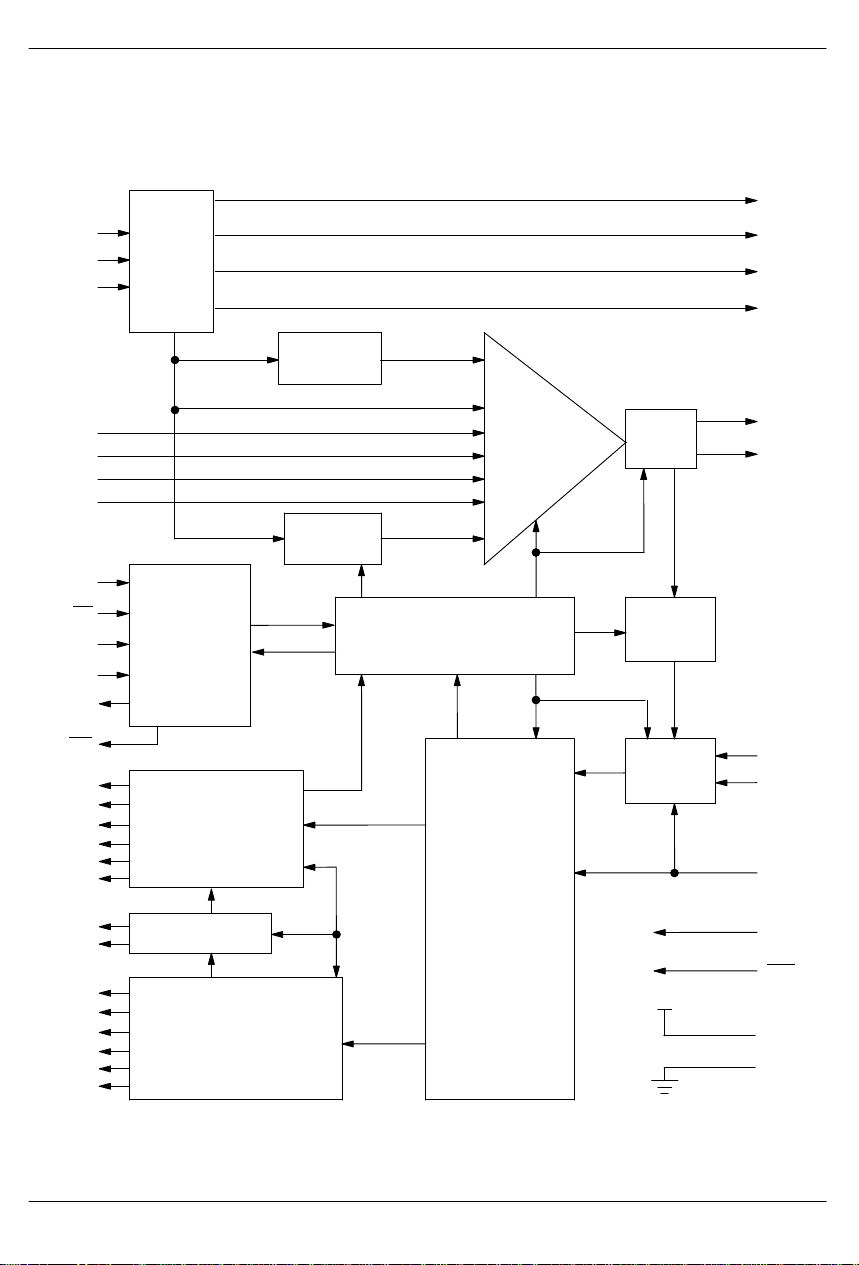
DS2181A BLOCK DIAGRAM Figure 1
TCLK
TFSYNC
TMSYNC
TSER
TSD
TIND
TXD
SPS
CS
SCLK
SDI
SDO
TRANSMIT
TIMING
SERIAL PORT/
HARDWARE
MODE CONTROL
LOGIC
ALIGN WORD
GENERAT OR
ALARM
GENERAT OR
CONTROL, STATUS AND ALARM
This mode requires no host processor and disables
special features available in the processor mode.
HDB3
CODER
LOOPBACK
REGISTERS
DATA
SELECTOR
TMO
TAF
TSTS
TCHCLK
TPOS
TNEG
INT
RDMA
RBV
RRA
RCL
RFER
RLOS
RSER
RSD
RFSYNC
RMSYNC
RCSYNC
RAF
RSTS
RCHCLK
041995 2/32
ALARM DETECTION
DATA DEMUX
RECEIVE TIMING
RECEIVE
SYNCHRONIZER/
SYNC CONTROLLER
HDB3
DECODER
RPOS
RNEG
RCLK
TEST
RST
VDD
VSS
Page 3

TRANSMIT PIN DESCRIPTION (40–PIN DIP ONLY) Table 1
PIN SYMBOL TYPE DESCRIPTION
1 TMSYNC I Transmit Multiframe Sync. Low-high transition establishes start of CAS and/or
2 TFSYNC I Transmit Frame Sync. Low-high transition every frame period establishes frame
3 TCLK I Transmit Clock. 2.048 MHz primary clock.
4 TCHCLK O Transmit Channel Clock. 256 KHz clock which identifies timeslot boundaries.
5 TSER I Transmit Serial Data. NRZ data input, sampled on falling edges of TCLK.
6 TMO O Transmit Multiframe Out. Output of multiframe counter; high during frame 0, low
7 TXD I Transmit Extra Data. Sampled on falling edge of TCLK during bit times 5, 7, and 8
8 TSTS O Transmit Signalling Timeslot. High during timeslot 16 of every frame, low other-
9 TSD I Transmit Signalling Data. CAS signalling data input; sampled on falling edges of
10 TIND I Transmit International and National Data. Sampled on falling edge of TCLK dur-
11 TAF O Transmit Alignment Frame. High during frames containing the frame alignment
1213TPOS
TNEG
CRC4 multiframe. Can be tied low, allowing internal multiframe counter to run free.
boundaries. Can be tied low, allowing TMSYNC to establish frame boundaries.
Useful for parallel-to-serial conversion of channel data.
otherwise.
of timeslot 16 in frame 0 when CAS signalling is enabled.
wise.
TCLK for insertion into outgoing timeslot 16 when enabled.
ing bit 1 time of timeslot 0 every frame (international) and/or during bit times 4
through 8 of timeslot 0 during non-align frames (national) when enabled.
signal, low otherwise.
O Transmit Bipolar Data Outputs. Updated on rising edge of TCLK.
DS2181A
SYNCHRONIZER STATUS PIN (44–PIN PLCC ONLY) Table 2A
PIN SYMBOL TYPE DESCRIPTION
3 RMSA O Receive Multiframe Search Active. This pin will transition high when the synchro-
nizer searching for the CAS multiframe alignment word is active.
6 RFSA O Receive Frame Search Active. This pin will transition high when the synchronizer
searching for the FAS is active.
25 RCTO O Receive CRC4 Time Out. This pin will transition high when the RCTO counter
reaches its maximum count of 32. The pin will return low when either the
DS2181AQ reaches CRC4 multiframe synchronization, or if CRC4 is disabled via
CRC.2, or if the device is issued a hardware reset via the RST
pin.
28 RCSA O Receive CRC4 Search Active. This pin will transition high when the synchronizer
searching for the CRC4 multiframe alignment word is active.
NOTES:
1. These output status pins are only available on the DS2181AQ.
2. If the TEST pin is tied low and CCR.1=0, then these pins will be tri–stated.
041995 3/32
Page 4

DS2181A
RECEIVE PIN DESCRIPTION (40–PIN DIP ONLY) Table 2B
PIN SYMBOL TYPE DESCRIPTION
21 RRA O Receive Remote Alarm. Transitions high when alarm detected; returns low when
22 RDMA O Receive Distant Multiframe Alarm. Transitions high when alarm detected; returns
23 RAF O Receive Alignment Frame. High during frames containing the frame alignment
24 RCLK I Receive Clock. 2.048 MHz primary clock.
25 RCHCLK O Receive Channel Clock. 256 KHz clock, identifies timeslot boundaries; useful for
26 RSER O Receive Serial Data. Received NRZ data, updated on rising edges of RCLK.
27 RFSYNC O Receive Frame Sync. Trailing edge indicates start of frame.
28 RMSYNC O Receive Multiframe Sync. Low-high transition indicates start of CAS multiframe;
29 RSD O Receive Signalling Data. Extracted timeslot 16 data; updated on rising edge of
30 RSTS O Receive Signalling Timeslot. High during timeslot 16 of every frame, low other-
31 RCSYNC O Receive CRC4 Sync. Low-high transition indicates start of CRC4 multiframe; held
33 RST I Reset. Must be asserted during device power-up and when changing to/from the
3435RPOS
RNEG
36 RCL O Receive Carrier Loss. Low-high transition indicates loss of carrier.
37 RBV O Receive Bipolar Violation. Pulses high during detected bipolar violations.
38 RFER O Receive Frame Error . Pulses high when frame alignment, CAS multiframe align-
39 RLOS O Receive Loss of Sync. Indicates synchronizer status; high when frame, CAS and/
alarm cleared.
low when alarm cleared.
signal, low otherwise.
serial-to-parallel conversion of channel data.
held high during frame 0.
RCLK.
wise.
high during CRC4 frames 0 thru 7 and held low during frames 8 through 15.
hardware mode.
I Receive Bipolar Data. Sampled on falling edges of RCLK. Tie together to receive
NRZ data and disable BPV monitor circuitry.
ment or CRC4 words received in error.
or CRC4 multiframe search underway, low otherwise.
PORT PIN DESCRIPTION (40–PIN DIP ONLY) Table 3
PIN SYMBOL TYPE DESCRIPTION
14 INT O Receive Alarm Interrupt. Flags host controller during alarm conditions. Active low;
15 SDI I Serial Data In. Data for on-chip control registers; sampled on rising edge of SCLK.
16 SDO O Serial Data Out. Control and status data from on-chip registers. Updated on falling
17 CS I Chip Select. Must be low to write or read the serial port.
18 SCLK I Serial Data Clock. Used to write or read the serial port registers.
19 SPS I Serial Port Select. Tie to VDD to select the serial port. Tie to VSS to select the
041995 4/32
open drain output.
edge of SCLK; tri-stated during port write or when CS
hardware mode.
is high.
Page 5

POWER AND TEST PIN DESCRIPTION (40–PIN DIP ONLY) T able 4
PIN SYMBOL TYPE DESCRIPTION
20 V
SS
– Signal Ground. 0.0 volts.
32 TEST I Test Mode. Tie to VSS to select the old DS2181 sync algorithm and to tri–
state the synchronizer status pins on the DS2181AQ. Tie to V
new DS2181A sync algorithm and activate the synchronizer status pins on the
to select the
DD
DS2181AQ.
40 V
DD
– Positive Supply. 5.0 volts.
REGISTER SUMMARY Table 5
REGISTER ADDRESS T/R
RIMR 0000 R Receive Interrupt Mask Register . Allows masking of alarm
RSR 0001 R
BVCR 0010 R Bipolar Violation Count Register . 8-bit presettable counter
CECR 0011 R CRC4 Error Count Register. 8-bit presettable counter which
FECR 0100 R Frame Error Count Register. 8-bit presettable counter which
RCR 0101 R Receive Control Register. Establishes receive side operating
CCR 0110 T/R Common Control Register. Establishes additional operating
TCR 0111 T Transmit Control Register. Establishes transmit side operation
TIR1
TIR2
TIR3
TIR4
1000
1001
1010
1011
TINR 1100 T Transmit International and National Register. When enabled
TXR 1101 T Transmit Extra Register. When enabled via the TCR, contents
1
DESCRIPTION/FUNCTION
generated interrupts.
2
Receive Status Register. Reports all receive alarm conditions.
which records individual bipolar violations.
records individual errors.
logs individual errors in the received frame alignment signal.
characteristics.
characteristics for transmit and receive sides.
characteristics.
T Transmit Idle Registers. Designates which outgoing timeslots
are to be substituted with idle code.
via the TCR, contents inserted into the outgoing national and/or
international bit positions.
inserted into the out going extra bit positions.
DS2181A
NOTES:
1. Transmit or receive side register .
2. RSR is a read-only register; all other registers are read/write.
3. Reserved bit locations must be programmed to 0.
041995 5/32
Page 6

DS2181A
SERIAL PORT INTERFACE
Pins 14 through 18 of the DS2181A serve as a microprocessor/microcontroller-compatible serial port. Fourteen
on-chip registers allow the user to update operational
characteristics and monitor device status via a host controller, minimizing hardware interfaces.
Port read/write timing is unrelated to the chip transmit
and receive timing, allowing asynchronous reads and/
or writes by the host. The timing set is identical to that of
8051-type microcontrollers operating in serial port
mode 0. For proper operation of the port and the transmit and receive registers, the user should provide TCLK
and RCLK as well as SCLK.
ADDRESS/COMMAND
An address/command byte write must precede any
read or write of the port registers. The first bit written
(LSB) of the address/command byte specifies read or
write. The following nibble identifies register address.
The next two bits are reserved and must be set to zero
for proper operation. The last bit of the address/command word enables the burst mode when set; the burst
mode allows consecutive reading or writing of all register data. Data is written to and read from the port LSB
first.
CHIP SELECT AND CLOCK CONTROL
All data transfers are initiated by driving the CS input
low. Data is sampled on the rising edge of SCLK. Data is
output on the falling edge of SCLK and held to the next
falling edge. All data transfers are terminated and SDO
tri-stated when CS returns to high.
CLOCKS
T o access the serial port registers both TCLK and RCLK
are required along with the SCLK. The TCLK and RCLK
are used to internally access the transmit and receive
registers, respectively. The CCR is considered a receive register for this purpose.
DATA I/O
Following the eight SCLK cycles that input the address/
command byte, data at SDI is strobed into the addressed register on the next eight SCLK cycles (register
write) or data is presented at SDO on the next eight
SCLK cycles (register read). SDO is tri-stated during
writes and may be tied to SDI in applications where the
host processor has bidirectional I/O capability.
BURST MODE
The burst mode allows all on-chip registers to be consecutively read or written by the host processor. This
feature minimizes device initialization time on system
power-up or reset. Burst mode is initiated when ACB.7
is set and the address nibble is 0000.
be read or written during the burst mode. If CS
tions high before the burst is complete, data validity is
not guaranteed.
All registers must
transi-
041995 6/32
Page 7
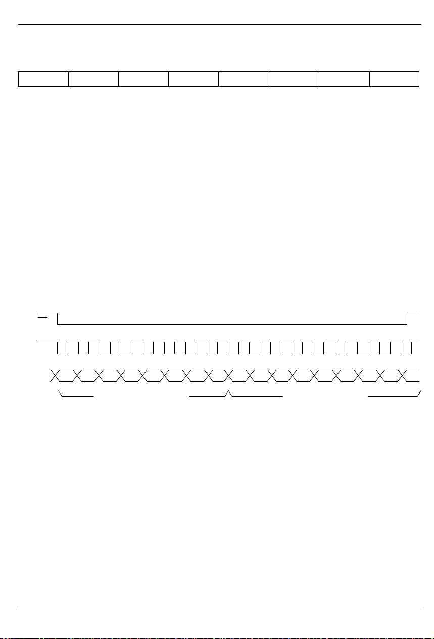
ACB: ADDRESS COMMAND BYTE Figure 2
(MSB) (LSB)
BM – – ADD3 ADD2 ADD1 ADD0 R/W
SYMBOL POSITION NAME AND DESCRIPTION
BM ACB.7 Burst Mode. If set (and ACB.1 through ACB.4 = 0), burst read or write is
enabled.
– ACB.6 Reserved; must be 0 for proper operation.
– ACB.5 Reserved; must be 0 for proper operation.
ADD3 ACB.4 MSB of register address.
ADD2 ACB.3
ADD1 ACB.2
ADD0 ACB.1 LSB of register address.
R/W ACB.0 Read/Write Select.
0 = Write address register.
1 = Read address register.
SERIAL PORT READ/WRITE Figure 3
DS2181A
CS
SCLK
SDI,SDO
ADD0 ADD1 ADD2 ADD3 0 0 BM D0 D1 D2 D3 D4 D5 D6 D7R/W
ADDRESS/COMMAND DATA INPUT/OUTPUT
NOTES:
1. SDI sampled on rising edge of SCLK.
2. SDO updated on falling edge of SCLK.
041995 7/32
Page 8

DS2181A
TCR: TRANSMIT CONTROL REGISTER Figure 4
(MSB) (LSB)
TUA1 TSS TSM INBS NBS XBS TSA1 ODM
SYMBOL POSITION NAME AND DESCRIPTION
TUA1 TCR.7 Transmit Unframed All 1’s.
0 = Normal operation.
1 = Replace outgoing data at TPOS and TNEG with unframed all 1’s code.
TSS TCR.6 Transmit Signalling Select
0 = Signalling data embedded in the serial bit stream is sampled at TSER
during timeslot 16.
1 = Signalling data is channel associated and sampled at TSD as shown in
Table 6.
TSM TCR.5 Transmit Signalling Mode
0 = Channel Associated Signalling (CAS).
1 = Common Channel Signalling (CCS).
INBS TCR.4 International Bit Select
0 = Sample international bit at TIND.
1 = Outgoing international bit = TINR.7.
NBS TCR.3 National Bit Select
0 = Sample national bits at TIND.
1 = Source outgoing national bits from TINR.4 through TINR.0.
XBS TCR.2 Extra Bit Select
0 = Sample extra bits at TXD.
1 = Source extra bits from TXR.0 through TXR.1 and TXR.3.
TSA1 TCR.1 Transmit Signalling All 1’s
0 = Normal operation.
1 = Force contents of timeslot 16 in all frames to all 1’s.
ODM TCR.0 Output Data Mode
0 = TPOS and TNEG outputs are 100% duty cycle.
1 = TPOS and TNEG outputs are 50% duty cycle.
1
1
NOTE:
1. When the common channel signalling mode is enabled (TCR.5 = 1), the TSD input is disabled internally; all
timeslot 16 data is sampled at TSER.
041995 8/32
Page 9

CCR: COMMON CONTROL REGISTER Figure 5
(MSB) (LSB)
– TAFP THDE RHDE TCE RCE SAS LLB
SYMBOL POSITION NAME AND DESCRIPTION
– CCR.7 Reserved; must be 0 for proper operation.
TAFP CCR.6 Transmit Align Frame Position
When clear, the CAS multiframe begins with a frame containing the frame
alignment signal. When set, the CAS multiframe begins with a frame not
containing the frame alignment signal.
THDE CCR.5 Transmit HDB3 Enable
0 = Outgoing data at TPOS and TNEG is AMI coded.
1 = Outgoing data at TPOS and TNEG is HDB3 coded.
RHDE CCR.4 Receive HDB3 Enable
0 = Incoming data at RPOS and RNEG is AMI coded.
1 = Incoming data is RPOS and RNEG is HDB3 coded.
TCE CCR.3 Transmit CRC4 Enable
When set, outgoing international bit positions in frames 0 through 12 and 14
are replaced by CRC4 multiframe alignment and checksum words.
RCE CCR.2 Receive CRC4 Enable
0 = Disable CRC4 multiframe synchronizer.
1 = Enable CRC4 synchronizer; search for CRC4 multiframe alignment
once frame alignment complete.
SAS CCR.1 Sync Algorithm Select
0 = Use old DS2181 sync algorithm
1 = Use new DS2181A sync algorithm
LLB CCR.0 Local Loopback
0 = Normal operation.
1 = Internally loop TPOS, TNEG, and TCLK to RPOS, RNEG, and RCLK.
1
DS2181A
NOTES:
1. This bit must be cleared when CRC4 multiframe mode is enabled (CCR.3 = 1); its state does not affect CCS
framing (RCR.5 = 1).
2. CCR is considered a receive register and operates from RCLK and SCLK.
041995 9/32
Page 10

DS2181A
RCR: RECEIVE CONTROL REGISTER Figure 6
(MSB) (LSB)
– – RSM CMSC CMRC FRC SYNCE RESYNC
SYMBOL POSITION NAME AND DESCRIPTION
– RCR.7 Reserved; must be 0 for proper operation.
– RCR.6 Reserved; must be 0 for proper operation.
RSM RCR.5 Received Signalling Mode
0 = Channel Associated Signalling (CAS).
1 = Common Channel Signalling (CCS).
CMSC RCR.4 CAS Multiframe Sync Criteria
0 = Declare sync when fixed sync criteria met.
1 = Declare sync when fixed criteria are met and two additional consecutive
valid multiframe alignment signals are detected.
CMRC RCR.3 CAS Multiframe Resync Criteria
0 = Utilize only fixed resync criteria.
1 = Resync if fixed criteria met and/or if two consecutive timeslot 16 words
have values of 0 in the first four MSB positions (0000xxxx).
FRC RCR.2 Frame Resync Criteria
0 = Utilize only fixed resync criteria.
1 = Resync if fixed criteria met and/or if bit 2 in timeslot 0 of non-align frames
is received in error on three consecutive occasions.
SYNCE RCR.1 Sync Enable
If clear, the synchronizer will automatically begin resync if error criteria are
met. If high, no auto resync occurs.
RESYNC RCR.0 Resync
When toggled low to high, the receive synchronizer will initiate immediately .
The bit must be cleared, then set again for subsequent resyncs.
CEPT FRAME STRUCTURE
The CEPT frame is made up of 32 8-bit channels (timeslots) numbered from 0 to 31. The frame alignment signal in bit positions 2 through 8 of timeslot 0 of every other
frame is independent of the various multiframe modes
described below. Outputs T AF and RAF indicate frames
which contain the alignment signal. Timeslot 0 of frames
not containing the frame alignment signal is used for
alarm and national data. See the separate DS2181A
CEPT Transceiver Application Note for more details.
CAS SIGNALLING
CEPT networks support Channel Associated Signalling
(CAS) or Common Channel Signalling (CCS). These
041995 10/32
signalling modes are independently selectable for
transmit and receive sides.
CAS (selected when TCR.5 = 0 and/or when RCR.5 = 0)
is a bit-oriented signalling technique which utilizes a
16-frame multiframe. The multiframe alignment signal
(0-hex), extra and alarm bits occupy timeslot 16 of frame
0. Timeslot 16 of the remaining 15 frames is reserved for
channel signalling data. Four signalling bits (A, B, C and
D) are transmitted once per multiframe as shown in Figure 7. Input TMSYNC establishes the transmitted CAS
multiframe position. Signalling data can be sourced
from input TSD (TCR.6 = 1) or multiplexed into TSER
(TCR.6 = 0).
Page 11

DS2181A
CCS SIGNALLING
CCS (selected when TCR.5 = 1 and/or when RCR.1 = 1)
utilizes all bit positions of timeslot 16 in every frame for
message-oriented signalling data transmission. In CCS
mode one can use either timeslot 16 or any one of the
other 30 data channels for message-oriented signalling.
The CCS mode has no multiframe structure and the insertion of CAS multiframe alignment, distant multiframe
alarm and/or extra bits into timeslot 16 is disabled.
TSER is the source of timeslot 16 data.
CRC4 CODING
The need for enhanced error monitoring capability and
additional protection against emulators of the frame
alignment word has led to the development of a cyclic
redundancy check (CRC) procedure. When enabled via
CCR.2 and/or CCR.3, CRC4 coding replaces the international bit positions in frames 0 through 12 and 14 with
a CRC4 multiframe alignment pattern and associated
checksum words. The CRC4 multiframe must begin
with a frame containing the frame alignment signal
(CCR.6 = 0). A rising edge at TMSYNC establishes the
CRC4 multiframe alignment (TMSYNC will also establish outgoing CAS multiframe alignment if enabled via
TCR.5).
Incoming CRC4 multiframe alignment is indicated by
RCSYNC. Detected CRC4 checksum errors are reported at output RFER and logged in the CECR.
RECEIVE SYNCHRONIZER
The fixed characteristics of the receive synchronizer
may be modified by use of programmable characteristics resident in the RCR and CCR. Sync criteria must be
met before synchronization is declared. Resync criteria
establish error occurrences which will cause an auto-resync event when enabled (RCR.1 = 0).
FIXED FRAME SYNC CRITERIA
Valid frame sync is assumed when the correct frame
alignment signal is present in frame N and frame N + 2
and not present in frame N + 1 (bit 2 of timeslot 0 of
Frame N + 1 is also checked for 1). CAS and/or CRC4
multiframe alignment search is initiated when the frame
search is complete if enabled via RCR.5 and/or CCR.2.
FIXED CAS MULTIFRAME SYNC CRITERIA
CAS multiframe sync is declared when the multiframe
alignment pattern is properly detected and timeslot 16 of
the previous frame contains code other than zeros. If no
valid pattern can be found in 12 to 14 milliseconds (no
time out period exists if CCR.1=1 or TEST=1), frame
search is restarted .
FIXED CRC4 MULTIFRAME SYNC CRITERIA
CRC4 multiframe sync is declared if at least two valid
CRC4 multiframe alignment signals are found within 12
to 14 milliseconds (8 ms if CCR.1=1 or TEST=1) after
frame alignment is completed. If not found within 12 to
14 milliseconds (8 ms if CCR.1=1 or TEST=1), frame
search is restarted. The search for the multiframe alignment signal is performed in timeslot 0 of frames not containing the frame alignment signal.
FIXED FRAME RESYNC CRITERIA
When enabled via RCR.1, the device will automatically
initiate frame search whenever the frame alignment
word is received in error three consecutive times.
FIXED CAS MULTIFRAME RESYNC CRITERIA
When enabled via RCR.1, the device will automatically
initiate frame search whenever two consecutive CAS
multiframe alignment words are received in error.
The receive synchronizer searches for the frame alignment pattern first. Once identified, the output timing set
associated with the framing pattern (all outputs except
RCSYNC and RMSYNC) is updated to that new alignment. If enabled, the synchronizer then begins CAS
and/or CRC4 multiframe search; outputs RMSYNC
and/or RCSYNC are then updated. Output RLOS is held
high during the entire resync process, then transitions
low after the last output timing update indicating resync
is complete. For more details about the receive synchronizer, see the separate DS2181A CEPT T ransceiver Application Note.
FIXED CRC4 RESYNC CRITERIA
If CCR.1=1 or if the TEST pin is tied high, then the
DS2181A will initiate the resync at the FAS level if 915 or
more CRC4 words out of 1000 are received in error.
CAS SIGNALLING SOURCE
CAS applications sample signalling data at TSER when
TCR.6 = 0; an on-chip data multiplexer accepts channel-associated data input at TSD when TCR.6 = 1. The
data multiplexer must be disabled (TCR.6 = 0) when the
CCS mode is enabled (TCR.5 = 1).
041995 11/32
Page 12

DS2181A
TSD INPUT TIMING (TCR.6 = 1; TCR.5 = 0) Table 6
FRAME # TIMESLOT SIGNALLING
DATA SAMPLED AT TSD
0 17
1 1,18
2 2,19
3 3,20
4 4,21
5 5,22
6 6,23
7 7,24
8 8,25
9 9,26
10 0,27
11 11,28
12 12,29
13 13,30
14 14,31
15 15
NOTE:
1. A, B, C and D data is sampled on falling edges of TCLK during bit times 5, 6, 7 and 8 of timeslots indicated.
TSD INPUT TIMING Figure 7
TCLK
TCHCLK
TIMESLOT 1 TIMESLOT 18
FRAME 1
TSD
041995 12/32
DON’T CARE DON’T CAREAB DCABDC
SAMPLED
FOR TIMESLOT 1
SAMPLED
FOR TIMESLOT 18
Page 13

CAS OUTPUT FORMAT IN TIMESLOT 16 Figure 8
DS2181A
Frame 0
0000XYXX
1
ABCD for
timeslot 1
Frame 1 Frame 15
ABCD for
timeslot 17
- - -
ABCD for
timeslot 15
ABCD for
timeslot 31
NOTE:
1. Timeslot 16 of frame 0 is reserved for the multiframe alignment word (0000), distant multiframe alarm (Y) and
extra bits (X-XX).
TINR: TRANSMIT INTERNATIONAL AND NATIONAL REGISTER Figure 9
(MSB) (LSB)
INB
SYMBOL POSITION NAME AND DESCRIPTION
INB TINR.7 International Bit. Inserted into the outgoing data stream when TCR.4 = 1.
– TINR.6 Reserved; must be 0 for proper operation.
TRA TINR.5 Transmit Remote Alarm
NB4 TINR.4 Transmit National Bits. Inserted into the outgoing data stream at TPOS
NB5 TINR.3
NB6 TINR.2
NB7 TINR.1
NB8 TINR.0
– TRA NB4 NB5 NB6 NB7 NB8
0 = Normal operation; bit 3 of timeslot 0 in non-alignment frame clear.
1 = Alarm condition; bit 3 of timeslot 0 in non-align frames set.
and TNEG when TCR.3 = 1.
TRANSMIT INTERNATIONAL AND
NATIONAL DATA
Bit 1 of timeslot 0 in all frames is known as the international bit. When TCR.4 = 1, the transmitted international
bit is sourced from TINR.7. When TCR.4 = 0, the transmitted international bit is sampled at TIND during the
first bit period of each frame. The international bit positions in all outgoing frames except 13 and 15 are replaced by CRC4 codewords and the CRC4 multiframe
alignment signal when CCR.3 = 1.
Bits 4 through 8 of timeslot 0 in non-align frames are reserved for national use. When TCR.3 = 1, the transmitted national bits are sourced from register locations
TINR.4 through TINR.0. If TCR.3 = 0, the national bits
are sampled at TIND during bit times 4 through 8 of
timeslot 0 in non-align frames.
Reserved bit positions in the TINR must be set to 0 when
written; those bits can be 0 or 1 when read.
041995 13/32
Page 14

DS2181A
TXR: TRANSMIT EXTRA REGISTER Figure 10
(MSB) (LSB)
– – – – XB1 TDMA XB2 XB3
SYMBOL POSITION NAME AND DESCRIPTION
– TXR.7 Reserved; must be 0 for proper operation.
– TXR.6 Reserved; must be 0 for proper operation.
– TXR.5 Reserved; must be 0 for proper operation.
– TXR.4 Reserved; must be 0 for proper operation.
XB1 TXR.3 Extra Bit 1
TDMA TXR.2 Transmit Distant Multiframe Alarm
0 = Normal operation; bit 6 of timeslot 16 in frame 0 clear.
1 = Alarm condition; bit 6 of timeslot 16 in frame 0 set.
XB2 TXR.1 Extra Bit 2
XB3 TXR.0 Extra Bit 3
TRANSMIT EXTRA DATA
In the CAS mode, timeslot 16 of frame 0 contains the
multiframe alignment pattern, extra bits and the distant
extra bits, alignment pattern and alarm signal are not utilized in the CCS mode (TCR.5 = 1); input TSER over-
writes all timeslot 16 bit positions.
multiframe alarm. When CAS is enabled (TCR.5 = 0),
the extra bits are sourced from TXR.0, TXR.1 and
TXR.3 (TCR.2 = 1) or the extra bits are sampled exter-
Reserved bit positions in the TXR must be set to 0 when
written; those bits can be 0 or 1 when read.
nally at TXD during the extra bit time (TCR.2 = 0). The
TIR1 - TIR4: TRANSMIT IDLE REGISTERS Figure 11
(MSB) (LSB)
TS7 TS6 TS5 TS4 TS3 TS2 TS1 TS0
1
TS15 TS14 TS13 TS12 TS11 TS10 TS9 TS8
TS23 TS22 TS21 TS20 TS19 TS18 TS17 TS16
1
TS31 TS30 TS29 TS28 TS27 TS26 TS25 TS24
SYMBOL POSITION NAME AND DESCRIPTION
TS31 TIR4.7 Transmit Idle Registers
TS0 TIR1.0 Each of these bit positions represents a timeslot in the outgoing stream at
TPOS and TNEG; when set, the contents of that timeslot are forced to idle
code (11010101).
NOTE:
1. TS0 and TS16 are not affected by the idle register.
TIR1
TIR2
TIR3
TIR4
041995 14/32
Page 15

DS2181A
TRANSMIT TIMING
A low-high transition at TMSYNC once per multiframe
(every 2 milliseconds) or at a multiple of the multiframe
rate establishes outgoing CAS and/or CRC4 multiframe
TMSYNC and/or TFSYNC can be tied low by the user, in
which case the arbitrary frame and multiframe alignment established by the device will be indicated at TMO
and TAF.
alignment. Output TMO indicates that alignment. A lowhigh transition at TFSYNC at the frame rate (125 us) or
at a multiple of the frame rate establishes the outgoing
frame position. Output TAF indicates that alignment.
Output TAF also indicates frames containing the frame
alignment signal. Those frames can be even or odd
numbering frames of the outgoing CAS multiframe
(CCR.6).
TRANSMIT MULTIFRAME TIMING Figure 12
0
FRAME #
TMSYNC
TMO
TFSYNC
1
TAF
2
TAF
123456789101112131415015
NOTES:
1. Alignment frames are even frames of the CAS and/or CRC4 multiframes (CCR.6 = 0).
2. Alignment frames are odd frames of the CAS multiframe (CCR.6 = 1).
041995 15/32
Page 16

DS2181A
TRANSMIT MULTIFRAME BOUNDARY TIMING Figure 13
TCLK
1
TMSYNC
TFSYNC
TAF
TCHCLK
TMO
,
2
1
TSER
TPOS
TNEG
MSB LSBLSB MSB
TIMESLOT 31 TIMESLOT 0
FRAME 15
3
TIMESLOT 30
LSB MSB LSB MSB
FRAME 0
TIMESLOT 31 TIMESLOT 0
FRAME 15
FRAME 0
NOTES:
1. Low-high transitions on TMSYNC and/or TFSYNC must occur one TCLK period early with respect to actual
frame and multiframe boundaries. TMO follows the rising edge of TMSYNC or TFSYNC.
2. TAF transitions on true frame boundaries.
3. Delay from TSER to TPOS, TNEG is five TCLK periods.
041995 16/32
Page 17

TRANSMIT SIGNALLING TIMESLOT TIMING Figure 14
TCLK
TCHCLK
TSTS
TIMESLOT 15 TIMESLOT 16 TIMESLOT 17
RECEIVE SIGNALLING
Receive signalling data is available at two outputs:
RSER and RSD. RSER outputs the signalling data in
timeslot 16 at RSER. The signalling data is also ex-
tracted from timeslot 16 and presented at RSD during
the timeslots shown in T able 7. This channel-associated
signalling simplifies CAS system design.
RECEIVE SIGNALLING Table 7
DS2181A
FRAME # RSD1 VALID DURING
TIMESLOT #
0 15,
1
-2
-2
,17
2 1,18
3 2,19
4 3,20
5 4,21
6 5,22
7 6,23
8 7,24
9 8,25
10 9,26
11 10,27
12 11,28
13 12,29
14 13,30
15 14,31
NOTES: (Applicable only to CAS systems.)
1. RSD is valid for the least significant nibble in each indicated timeslot. Timeslot A data appears in bit 5, B in bit
6, C in bit 7 and D in bit 8.
2. RSD does not output valid data during timeslots 0 and 16.
041995 17/32
Page 18

DS2181A
RECEIVE MULTIFRAME TIMING Figure 15
RCLK
RCHCLK
TIMESLOT 1 TIMESLOT 18
FRAME 2
RSD
DATA VALID
FOR TIMESLOT 1
RECEIVE TIMING
The receive side output timing set is identical to that
found on the transmit side. The user can tie receive outputs directly to the transmit inputs for drop and insert
NOT VALIDNOT VALID ABCD
applications. The received data of RPOS, RNEG appear at RSER after six RCLK delays, without any
change except for the HDB3-to-NRZ conversion when
HDB3 is enabled.
AB DC
DATA VALID
FOR TIMESLOT 18
NOTE:
1. The CAS multiframe can start with an align or non-align frame. The CRC4 multiframe always starts with an
align frame.
RSD TIMING Figure 16
0
FRAME #
RFSYNC
RMSYNC
RAF
1
123456789101112131415015
RCSYNC
041995 18/32
Page 19

RECEIVE MULTIFRAME BOUNDARY TIMING Figure 17
DS2181A
RNEG,
RPOS
RCLK
RFSYNC
RCHCLK
RMSYNC
RCSYNC
RAF
RSER
LSB MSB
TIMESLOT 0
FRAME 0
1
4
,
2
3
MSB
TIMESLOT 31 TIMESLOT 0
FRAME 15
LSB MSB
TIMESLOT 1
LSB MSBLSB MSB
FRAME 0
NOTES:
1. Low-high transitions on RMSYNC and RFSYNC occur one RCLK period early with respect to actual frame
and multiframe boundaries.
2. RAF transitions on true frame boundaries.
3. Delay from RPOS, RNEG to RSER is six RCLK periods.
4. RMSYNC and RCSYNC transition low on the falling edge of RFSYNC.
041995 19/32
Page 20

DS2181A
RSR: RECEIVE STATUS REGISTER Figure 18
(MSB) (LSB)
RRA RDMA RSA1 RUA1 FSERR MFSERR RLOS ECS
SYMBOL POSITION NAME AND DESCRIPTION
RRA RSR.7 Receive Remote Alarm. Set when bit 3 of timeslot 0 in non-align frames
set for three consecutive non-align frames.
RDMA RSR.6 Receive Distant Multiframe Alarm. Set when bit 6 of timeslot 16 in frame
0 is set for three consecutive multiframes.
RSA1 RSR.5 Receive Signalling All Ones. Set when the contents of timeslot 16 have
been all ones for two consecutive frames.
RUA1 RSR.4 Receive Unframed All Ones. Set when less thant three zeros have been
received in the last two consecutive frames.
FSERR RSR.3 Frame Resync Criteria Met. Set when the frame error criteria are met;
also the frame resync is initiated if RCR.1=0.
MFSERR RSR.2 CAS Multiframe Resync Criteria Met. Set when the CAS multiframe error
criteria are met; also, the frame resync is initiated if RCR.1=0.
RLOS RSR.1 Receive Loss of Sync. Set when resync is in progress.
ECS RSR.0 Error Counter Saturation. Set when any of the on-chip counters at FECR,
CECR or BVCR saturates.
NOTE:
1. When in the CCS mode, the RDMA flag bit and the RDMA pin have no significance. It will be set when bit 6 of
timeslot 16 in frame 0 is set for three consecutive multiframes in either CAS or CCS mode.
041995 20/32
Page 21

RIMR: RECEIVE INTERRUPT MASK REGISTER Figure 19
(MSB) (LSB)
RRA RDMA RSA1 RUA1 FSERR MFSERR RLOS ECS
SYMBOL POSITION NAME AND DESCRIPTION
RRA RIMR.7 Receive Remote Alarm
1 = Interrupt enabled
0 = Interrupt masked
RDMA RIMR.6 Receive Distant Multiframe Alarm
1 = Interrupt enabled
0 = Interrupt masked
RSA1 RIMR.5 Receive Signalling All 1’s
1 = Interrupt enabled
0 = Interrupt masked
RUA1 RIMR.4 Receive Unframed All 1’s
1 = Interrupt enabled
0 = Interrupt masked
FSERR RIMR.3 Frame Resync Criteria Met
1 = Interrupt enabled
0 = Interrupt masked
MFSERR RIMR.2 CAS Multiframe Resync Criteria Met
1 = Interrupt enabled
0 = Interrupt masked
RLOS RIMR.1 Receive Loss of Sync
1 = Interrupt enabled
0 = Interrupt masked
ECS RIMR.0 Error Count Saturation
1 = Interrupt enabled
0 = Interrupt masked
DS2181A
ALARM REPORTING AND INTERRUPT
SERVICING
Alarm and error conditions are reported at outputs and
the RSR. Use of the RSR and error count registers simplifies system error monitoring. The RSR can be read in
one of two ways: a burst read does not disturb the RSR
contents; a direct read will clear all bits set in the RSR
unless the alarm condition which set them is still active.
Interrupts are enabled via the RIMR and are generated
whenever an alarm or error condition sets an RSR bit.
The host controller must service the transceiver in order
to clear an interrupt condition. Clearing the appropriate
RIMR bit will unconditionally clear an interrupt.
041995 21/32
Page 22

DS2181A
BVCR: BIPOLAR VIOLATION COUNT REGISTER Figure 20
(MSB) (LSB)
BVD7 BVD6 BVD5 BVD4 BVD3 BVD2 BVD1 BVD0
SYMBOL POSITION NAME AND DESCRIPTION
BVD7 BVCR.7 MSB of bipolar violation count.
BVD0 BVCR.0 LSB of bipolar violation count.
CECR: CRC4 ERROR COUNT REGISTER Figure 21
(MSB) (LSB)
CRC7 CRC6 CRC5 CRC4 CRC3 CRC2 CRC1 CRC0
SYMBOL POSITION NAME AND DESCRIPTION
CRC7 BVCR.7 MSB of CRC4 error count.
CRC0 BVCR.0 LSB of CRC4 error count.
FECR: FRAME ERROR COUNT REGISTER Figure 22
(MSB) (LSB)
FE7 FE6 FE5 FE4 FE3 FE2 FE1 FE0
SYMBOL POSITION NAME AND DESCRIPTION
FE7 FECR.7 MSB of frame error count.
FE0 FECR.0 LSB of frame error count.
ERROR LOGGING
The BVCR, CECR and FECR contain 8-bit binary up
counters which increment on individual bipolar violations, CRC4 code word errors (when CCR.2 = 1), and
word errors in the frame alignment signal. Each counter
saturates at 255. Once saturated, each following error
occurrence will generate an interrupt (RIMR.0 = 1) until
the register is reprogrammed to a value other than FF
(hex). Presetting the registers allows the user to establish specific error count thresholds; the counter will
count up to saturation from the preset value. The BVCR
increments at all times (regardless of sync status),
except when HDB3 code words are received with
CCR.4=1. CECR and FECR increments are disabled
whenever resync is in progress (RLOS high).
041995 22/32
ALARM OUTPUTS
Alarm conditions are also reported real time at alarm
outputs. These outputs can be used with off-chip logic to
complement the on-chip error reporting capability of the
DS2181A. In the hardware mode, they are the only
alarm reporting means available.
RLOS
The RLOS output indicates the status of the receive
synchronizer. When high, frame, CAS multiframe and/
or CRC4 multiframe synchronization is in progress. A
high-low transition indicates resync is complete. The
RLOS bit (RSR.1) is a latched version of the RLOS output.
Page 23

DS2181A
RRA
The remote alarm output transitions high when a remote
The RDMA bit (RSR.6) is a latched version of the RDMA
output.
alarm is detected. A high-low transition indicates the
alarm condition has been cleared. The alarm condition
is defined as bit 3 of time slot 0 set for three consecutive
non-align frames. The alarm state is cleared when bit 3
has been clear for three consecutive non-align frames.
The RRA bit (RSR.7) is a latched version of the RRA
RCL
RCL transitions high after 32 consecutive zeros appear
at RPOS and RNEG; it goes low at the next one occur-
rence.
output.
RFER
RBV
RBV pulses high when the accused bit emerges at
RSER. RBV will return low when RCLK goes low. Bipolar violations are also logged in the BVCR. The RBV pin
provides a pulse for every violation which can be
counted externally .
RDMA
RDMA transitions high when bit 6 of timeslot 16 in frame
0 is set for three consecutive occasions and returns low
when the bit is clear for three consecutive occasions.
The RFER output transitions high when received frame
alignment, CAS multiframe alignment and/or CRC4
code words are in error. The FECR and CECR log error
events reported at this output. FECR logs only the frame
alignment word errors. CECR logs CRC4 code word er-
rors.
T o complement the on-chip error logging capabilities of
the DS2181A, the system designer can use off-chip log-
ic gated by receive side outputs RCHCLK, RAF, RSTS
and RCSYNC to demux error states present at RFER.
See the separate DS2181A CEPT Transceiver Application
Note for more details.
RFER OUTPUT TIMING FOR ALL ERROR CONDITIONS Figure 23
RFSYNC
RAF
RMSYNC
RCSYNC
123 4
RFER
CAS MULTIFRAME ALIGNMENT ERROR Figure 24
RCLK
RCHCLK
RSTS
1
RFER
041995 23/32
Page 24

DS2181A
CRC4 SUB-MULTIFRAME 2 ERRORED Figure 25
RCLK
RCHCLK
RFSYNC
RAF
RCSYNC
RFER2
FRAME ALIGNMENT WORD ERRORED Figure 26
RCLK
RCHCLK
RFSYNC
RAF
3
RFER
CRC4 SUB-MULTIFRAME 1 ERRORED Figure 27
RCLK
RCHCLK
RFSYNC
RAF
RCSYNC
4
RFER
041995 24/32
Page 25

DS2181A
NOTES FOR FIGURES 23 THROUGH 27:
1. CAS multiframe alignment word received in error; RFER will transition high at first error occurrence and re-
main high as shown.
2. Previous CRC4 sub-multiframe 2 errored.
3. Frame alignment word errored.
4. Previous CRC4 sub-multiframe 1 errored.
RESET
A high-low transition on RST clears all internal registers
except the three error counters; a resync is initiated until
RST returns high. RST must be held low on system
power-up and when switching to/from the hardware
mode. Following reset, the host processor should update all on-chip registers to establish desired operating
modes.
do not require the features of the serial port. Tying SPS
low disables the serial port, clears all internal register lo-
cations except those shown below, and redefines pins
14 through 18 as mode control inputs. The mode control
inputs establish device operational characteristics as
shown in T able 8. The hardware mode simplifies device
retrofit into existing applications where control inter-
faces are designed with discrete logic.
HARDWARE MODE
An on-chip hardware control mode simplifies preliminary system prototyping and serves applications which
HARDWARE MODE CONTROL Table 8
PIN NUMBER REGISTER LOCATION NAME AND DESCRIPTION
14
(16)
15
(17)
16
(18)
17
(19)
18
(20)
TINR.5 TRA - Transmit Remote Alarm
0 = Normal operation
1 = Enable alarm
TXR.2 TDMA - Transmit Distant Multiframe Alarm
0 = Normal operation
1 = Enable alarm
CCR.5/CCR.4 Data Format
0 = Input and output data AMI coded
1 = Input and output data HDB3 coded
CCR.3/CCR.2 Transmit and Receive CRC4 Multiframe
0 = Disabled
1 = Enabled
TCR.5/RCR.5 Transmit and Receive CAS Multiframe
0 = Enabled
1 = Disabled
NOTE:
1. Pin numbers for PLCC package are listed in parenthesis.
041995 25/32
Page 26

DS2181A
ABSOLUTE MAXIMUM RATINGS*
Voltage on Any Pin Relative to Ground -1.0V to 7.0V
Operating Temperature 0°C to +70°C
Storage Temperature -55°C to 125°C
Soldering Temperature 260°C for 10 seconds
* This is a stress rating only and functional operation of the device at these or any other conditions above
those indicated in the operation sections of this specification is not implied. Exposure to absolute maximum rating conditions for extended periods of time may affect reliability.
RECOMMENDED DC OPERATING CONDITIONS (0°C to 70°C)
PARAMETER SYMBOL MIN TYP MAX UNITS NOTES
Logic 1 V
Logic 0 V
Supply V
IH
IL
DD
2.0 VDD+.3 V
-0.3 +0.8 V
4.5 5.5 V
DC ELECTRICAL CHARACTERISTICS (0°C to 70°C, VDD=5V + 10%)
PARAMETER SYMBOL MIN TYP MAX UNITS NOTES
Supply Current I
Input Leakage I
Output Current @ 2.4V I
Output Current @ 0.4V I
Output Leakage I
DD
OH
OL
LO
IL
-1.0 +1.0 µA 3
-1.0 mA 4
+4.0 mA 5
-1.0 +1.0 µA 6
6 10 mA 1,2
NOTES:
1. TCLK = RCLK = 2.048 MHz.
2. Outputs open.
3. 0V < V
4. All outputs except INT
5. All outputs.
6. Applies to SDO when tri-stated.
041995 26/32
< VDD.
IN
which is open collector.
Page 27

SERIAL PORT WRITE AC TIMING DIAGRAM Figure 28
CS
t
CWH
DS2181A
t
t
CC
t
CH
R
SCLK
t
t
DC
CL
SDI
t
CDH
NOTE:
1. Shaded regions indicate “don’t care” states of input data.
SERIAL PORT READ1 AC TIMING Figure 29
CS
SCLK
t
CDV
SDO
t
F
t
CCH
t
CDZ
High Z
NOTE:
1. Serial port write must precede a port read to provide address information.
041995 27/32
Page 28

DS2181A
AC ELECTRICAL CHARACTERISTICS
1,2
SERIAL PORT (0°C to 70°C, VDD = 5V + 5%)
PARAMETER SYMBOL MIN TYP MAX UNITS NOTES
SDI to SCLK Setup t
SCLK to SDI Hold t
CDH
SCLK Low Time t
SCLK High Time t
SCLK Rise and Fall Times tR,t
CS to SCLK Setup t
SCLK to CS Hold t
CS Inactive Time t
SCLK to SDO Valid t
CS to SDO High Z t
CCH
CWH
CDV
CDZ
DC
CL
CH
F
CC
50 ns
50 ns
244 ns
244 ns
100 ns
50 ns
50 ns
2.5 us
200 ns
75 ns
NOTES:
1. Measured at VIH = 2.0 or VIL = .8 and 10 ns maximum rise and fall time.
2. Output load capacitance = 100 pF.
AC ELECTRICAL CHARACTERISTICS
PARAMETER SYMBOL MIN TYP MAX UNITS NOTES
TCLK Period t
TCLK Pulse Width tWL,t
TCLK Rise and Fall Times tR,t
TSER, TSD, TIND and TXD Setup
to TCLK Falling
TSER, TSD, TIND and TXD Hold to
TCLK Falling
TFSYNC, TMSYNC Setup to TCLK
Falling
TFSYNC, TMSYNC Hold to TCLK
Falling
Propagation Delay TCLK to
TCHCLK, TSTS, TMO, TAF
1,2
TRANSMIT (0°C to 70°C, VDD = 5V + 5%)
488 ns
244 ns
20 ns
75 ns
t
STD
t
HTD
t
STS
t
HTS
t
PTS
p
WH
F
50 ns
50 ns
75 ns
50 ns
NOTES:
1. Measured at VIH = 2.0 or VIL = .8 and 10 ns maximum rise and fall time.
2. Output load capacitance = 100 pF.
041995 28/32
Page 29

DS2181A
AC ELECTRICAL CHARACTERISTICS
1,2
RECEIVE (0°C to 70°C, VDD = 5V + 5%)
PARAMETER SYMBOL MIN TYP MAX UNITS NOTES
Propagation Delay RCLK to
RMSYNC, RFSYNC, RSTS,
t
PRS
75 ns
RCHCLK, RAF
Propagation Delay RCLK to RSER,
RSD
Transition Time All Outputs t
RCLK Period t
RCLK Pulse Width tWL,t
RCLK Rise and Fall Times tR,t
RPOS, RNEG Setup to RCLK Fall-
ing
RPOS, RNEG Hold to RCLK Fall-
ing
Propagation Delay RCLK to RLOS,
RRA, RBV, RFER,RDMA, RCL
Minimum RST Pulse Width t
t
PRD
TTR
t
SRD
t
HRD
t
PRA
RST
75 ns
20 ns
P
WH
F
488 ns
244 ns
20 ns
50 ns
50 ns
75 ns
1 µs
NOTES:
1. Measured at VIH = 2.0 or VIL = .8 and 10 ns. maximum rise and fall time.
2. Output load capacitance = 100 pf.
CAPACITANCE (tA = 25°C)
PARAMETER SYMBOL MIN TYP MAX UNITS NOTES
Input Capacitance C
Output Capacitance C
IN
OUT
5 pF
7 pF
041995 29/32
Page 30

DS2181A
TRANSMIT AC TIMING DIAGRAM Figure 30
TCLK
t
P
t
WH
t
WL
t
F
t
R
TSER, TSD,
TIND, TXD
t
STD
t
HTD
t
STS
TFSYNC, TMSYNC
TCHCLK, TSTS,
TMO, TAF
RECEIVE AC TIMING DIAGRAM Figure 31
RCLK
t
PRD
RSER, RSD
t
PTS
t
HTS
t
P
t
WH
t
WL
t
R
t
F
RMSYNC,
RFSYNC,
RCSYNC,
RAF,RSTS,
RCHCLK
RCL,RBV,
RLOS,RDMA,
RRA,RFER
RST
RPOS, RNEG
041995 30/32
t
RST
t
PRS
t
PRA
t
SRDtHRD
Page 31

DS2181A CEPT TRANSCEIVER (600 MIL DIP) 40–PIN
N
B
D
DS2181A
1
KG H
INCHES
DIM MIN MAX
A 2.050 2.075
B 0.530 0.550
C 0.140 0.160
D 0.600 0.625
E 0.015 0.040
F 0.120 0.145
G 0.090 0.110
H 0.625 0.675
J 0.008 0.012
K 0.015 0.022
N 40
A
E
C
F
J
041995 31/32
Page 32

DS2181A
DS2181AQ CEPT TRANSCEIVER (PLCC)
E
E1
B
N
1
NOTE 1
CH1
NOTE1: PIN 1 IDENTIFIER TO BE LOCA TED IN ZONE INDICATED.
DIM MIN MAX
A 0.165 0.180
A1 0.090 0.120
A2 0.020 –
B 0.026 0.033
B1 0.013 0.021
C 0.009 0.012
CH1 0.042 0.048
D 0.685 0.695
D1 0.650 0.656
D2 0.590 0.630
E 0.685 0.695
E1 0.650 0.656
E2 0.590 0.630
e1 0.050 BSC
N 44 –
.150
MAX
INCHES
.075 MAX
E2
D1
D
e1
D2
B1
C
A1A2
A
041995 32/32
 Loading...