

Page 1
DS2180A
DS2180A
T1 Transceiver
FEATURES
• Single chip DS1 rate transceiver
• Supports common framing standards
– 12 frames/superframe “193S”
– 24 frames/superframe “193E”
• Three zero suppression modes
– B7 stuffing
– B8ZS
– Transparent
• Simple serial interface used for configuration, control
and status monitoring in “processor” mode
• “Hardware” mode requires no host processor; in-
tended for stand-alone applications
• Selectable 0, 2, 4, 16 state robbed bit signaling modes
• Allows mix of “clear” and “non-clear” DS0 channels on
same DS1 link
• Alarm generation and detection
• Receive error detection and counting for transmission
performance monitoring
• 5V supply, low-power CMOS technology
• Surface mount package available, designated
DS2180AQ
• Industrial temperature range of -40°C to +85°C avail-
able, designated DS2180AN or DS2180AQN
• Compatible to DS2186 Transmit Line Interface,
DS2187 Receive Line Interface, DS2188 Jitter Attenuator, DS2175 T1/CEPT Elastic Store, DS2290 T1
Isolation Stik, and DS2291 T1 Long Loop Stik
DESCRIPTION
The DS2180A is a monolithic CMOS device designed to
implement primary rate (1.544 MHz) T -carrier transmission systems. The 193S framing mode is intended to
support existing Ft/Fs applications (12 frames/superframe). The 193E framing mode supports the extended
superframe format (24 frames/superframe). Clear
channel capability is provided by selection of appropriate zero suppression and signaling modes.
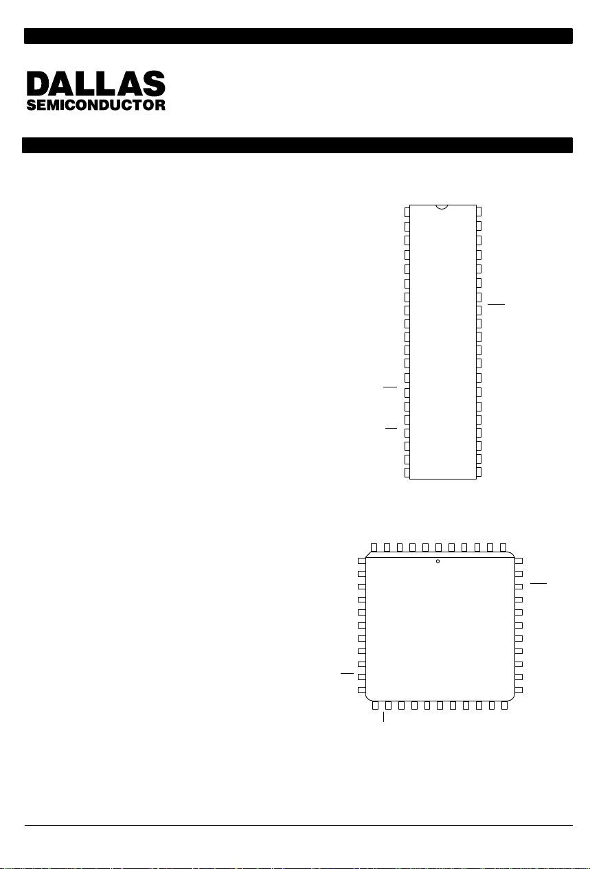
PIN ASSIGNMENT
TMSYNC
TFSYNC
TCLK
TCHCLK
TSER
TMO
TSIGSEL
TSIGFR
TABCD
TLINK
TLCLK
TPOS
TNEG
INT
SDI
SDO
CS
SCLK
SPS
VSS
40-Pin DIP (600 MIL)
NC
TCHCLK
TCLKNCTFSYNC
TSER
TSIGSEL
TSIGFR
TABCD
TLINK
TLCLK
TPOS
TNEG
6543214443424140
7
TMO
8
9
10
11
12
13
14
15
16
INT
17
SDI
18 19 20 21 22 23 24 25 26 27 28
CS
SDO
SCLK
1
2
3
4
5
6
7
8
9
10
11
12
13
14
15
16
17
18
19
20 21
TMSYNC
VDD
44-PIN PLCC
SPS
VSS
RYEL
40
39
38
37
36
35
34
33
32
31
30
29
28
27
26
25
24
23
22
RLOS
NC
RLINK
VDD
RLOS
RFER
RBV
RCL
RNEG
RPOS
RST
TEST
RSIGSEL
RSIGFR
RABCD
RMSYNC
RFSYNC
RSER
RCHCLK
RCLK
RLCLK
RLINK
RYEL
RFER
RBV
RCLK
RLCLK
39
38
37
36
35
34
33
32
31
30
29
RCL
RNEG
RPOS
RST
TEST
RSIGSEL
RSIGFR
RABCD
RMSYNC
RFSYNC
RSER
RCHCLK
NC
Copyright 1995 by Dallas Semiconductor Corporation.
All Rights Reserved. For important information regarding
patents and other intellectual property rights, please refer to
Dallas Semiconductor data books.
041995 1/36
Page 2
DS2180A
Several functional blocks exist in the transceiver. The
transmit framer/formatter generates appropriate framing bits, inserts robbed bit signaling, supervises zero
suppression, generates alarms, and provides output
clocks useful for data conditioning and decoding.
The receive synchronizer establishes frame and multiframe boundaries by identifying frame signaling bits, extracts signaling data, reports alarms and transmission
errors, and provides output clocks useful for data conditioning and decoding.
The control block is shared between transmit and receive sides. This block determines the frame, zero sup-
DS2180A BLOCK DIAGRAM Figure 1
TMSYNC
TFSYNC
TCLK
TLCLK
TLINK
TSER
TABCD
Transmit
Timing
F-Bit
Data
Yellow
Alarm
pression, alarm and signaling formats. User access to
the control block is by one of two modes.
In the processor mode, pins 14 through 18 are a microprocessor/microcontroller-compatible serial port which
can be used for device configuration, control and status
monitoring.
In the hardware mode, no offboard processor is required. Pins 14 through 18 are reconfigured into “hardwired” select pins. Features such as selection “clear”
DS0 channels, insertion of idle code and alteration of
sync algorithm are unavailable in the hardware mode.
TSIGSEL
TMO
TCHCLK
TSIGFR
Data
Selector
Bipolar
Coder
TPOS
TNEG
SCLK
RSER
RYEL
RABCD
RLINK
RLCLK
RSIGFR
RSIGSEL
RCHCLK
RMSYNC
RFSYNC
041995 2/36
INT
CS
SDI
SDO
SPS
Serial
Control
Interface
Yellow
Alarm
Detect
Data
Demux
Receive
Timing
Code
Gen
Information
Registers
Receive
Sync
Controller
Synchronizer
CRC
Bipolar
Coder
CRC
VDD
VSS
RST
TEST
RLOS
RBV
RCL
RPOS
RNEG
RCLK
RFER
Page 3

TRANSMIT PIN DESCRIPTION (40–PIN DIP ONLY) Table 1
PIN SYMBOL TYPE DESCRIPTION
1 TMSYNC I Transmit Multiframe Sync. May be pulsed high at multiframe boundaries
2 TFSYNC I Transmit Frame Sync. Rising edge identifies frame boundary; may be
3 TCLK I Transmit Clock. 1.544 MHz primary clock.
4 TCHCLK O Transmit Channel Clock. 192 KHz clock which identifies time slot (channel)
5 TSER I Transmit Serial Data. NRZ data input, sample on falling edge of TCLK.
6 TMO O Transmit Multiframe Out. Output of internal multiframe counter indicates
7 TSIGSEL O Transmit Signaling Select. .667 KHz clock which identifies signaling frame
8 TSIGFR O Transmit Signaling Frame. High during signaling frames, low otherwise.
9 TABCD I Transmit ABCD Signaling. When enabled via TCR.4, sampled during
10 TLINK I T ransmit Link Data. Sampled during the F-bit time (falling edge of TCLK) of
11 TLCLK O Transmit Link Clock. 4 KHz demand clock for TLINK input.
12
13
TPOS
TNEG
to reinforce multiframe alignment or tied low, which allows internal multiframe
counter to free run.
pulsed every frame to reinforce internal frame counter or tied low (allowing
TMSYNC to establish frame and multiframe alignment).
boundaries. Useful for parallel-to-serial conversion of channel data.
multiframe boundaries. 50% duty cycle.
A and C in 193E framing. 1.33 KHz clock in 193S.
channel LSB time in signaling frames on falling edge of TCLK.
odd frames for insertion into the outgoing data stream (193E-FDL insertion).
Sampled during the F-bit time of even frames for insertion into the outgoing
data (193S-External S-Bit insertion).
O Transmit Bipolar Data Outputs. Updated on rising edge of TCLK.
DS2180A
PORT PIN DESCRIPTION (40–PIN DIP ONLY) Table 2
PIN SYMBOL TYPE DESCRIPTION
14 INT
1
O Receive Alarm Interrupt. Flags host controller during alarm conditions. Ac-
tive low, open drain output.
15 SDI
16 SDO
1
1
I Serial Data In. Data for onboard registers. Sampled on rising edge of SCLK.
O Serial Data Out. Control and status information from onboard registers. Up-
dated on falling edge of SCLK, tri-stated during serial port write or when CS
is high.
17 CS
18 SCLK
1
1
I Chip Select. Must be low to write or read the serial port registers.
I Serial Data Clock. Used to write or read the serial port registers.
19 SPS I Serial Port Select. T ie to VDD to select serial port. Tie to VSS to select hard-
ware mode.
NOTE:
1. Multifunction pins. See “Hardware Mode Description.”
041995 3/36
Page 4

DS2180A
POWER AND TEST PIN DESCRIPTION (40–PIN DIP ONLY) Table 3
PIN SYMBOL TYPE DESCRIPTION
20 V
SS
– Signal Ground. 0.0 volts.
32 TEST I Test Mode. T ie to VSS for normal operation.
40 V
DD
– Positive Supply. 5.0 volts.
RECEIVE PIN DESCRIPTION (40–PIN DIP ONLY) Table 4
PIN SYMBOL TYPE DESCRIPTION
21 RYEL O Receive Yellow Alarm. Transitions high when yellow alarm detected, goes
22 RLINK O Receive Link Data. Updated with extracted FDL data one RCLK before start
23 RLCLK O Receive Link Clock. 4 KHz demand clock for RLINK.
24 RCLK I Receive Clock. 1.544 MHz primary clock.
25 RCHCLK O Receive Channel Clock. 192 KHz clock identifies time slot (channel) bound-
26 RSER O Receive Serial Data. Received NRZ serial data, updated on rising edges of
27 RFSYNC O Receive Frame Sync. Extracted 8 KHz clock, one RCLK wide, indicates F-
28 RMSYNC O Receive Multiframe Sync. Extracted multiframe sync; edge indicates start
29 RABCD O Receive ABCD Signaling. Extracted signaling data output, valid for each
30 RSIGFR O Receive Signaling Frame. High during signaling frames, low during resync
31 RSIGSEL O Receive Signaling Select. In 193E framing a .667 KHz clock which identi-
33 RST I Reset. A high-low transition clears all internal registers and resets receive
34
35
RPOS
RNEG
36 RCL O Receive Carrier Loss. High if 32 consecutive 0’s appear at RPOS and
37 RBV O Receive Bipolar Violation. High during accused bit time at RSER if bipolar
38 RFER O Receive Frame Error. High during F-Bit time when FT or FS errors occur
39 RLOS O Receive Loss of Sync. Indicates sync status; high when internal resync is
low when alarm clears.
of odd frames (193E) and held until next update. Updated with extracted S-bit
data one RCLK before start of even frames (193S) and held until next update.
aries.
RCLK.
Bit position in each frame.
of multiframe, 50% duty cycle.
channel time in signaling frames. In non-signaling frames, RABCD outputs
the LSB of each channel word.
and non-signaling frames.
fies signaling frames A and C. A 1.33 KHz clock in 193S.
side counters. A high-low-high transition will initiate a receive resync.
Receive Bipolar Data Inputs. Samples on falling edge of RCLK. Tie togeth-
er to receive NRZ data and disable bipolar violation monitoring circuitry.
I
RNEG; goes low after next 1.
violation detected, low otherwise.
(193S) or when FPS or CRC errors occur (193E). Low during resync.
in progress, low otherwise.
041995 4/36
Page 5

REGISTER SUMMARY Table 5
REGISTER ADDRESS T/R
RSR 0000 R2Receive Status Register. Reports all receive alarm conditions.
RIMR 0001 R Receive Interrupt Mask Register. Allows masking of individual alarm-gen-
BVCR 0010 R Bipolar Violation Count Register. 8-bit presettable counter which records
ECR 0011 R Error Count Register. Two independent 4-bit counters which record OOF
3
CCR
RCR
TCR
TIR1
TIR2
TIR3
TTR1
TTR2
TTR3
RMR1
RMR2
RMR3
3
3
0100 T/R Common Control Register. Selects device operating characteristics com-
0101 R Receive Control Register. Programs device operating characteristics
0110 T Transmit Control Register. Selects additional transmit side modes.
0111
1000
1001
1010
1011
1100
1101
1110
1111
1
DESCRIPTION/FUNCTION
erated interrupts.
individual bipolar violations.
occurrences and individual frame bit or CRC errors.
mon to receive and transmit sides.
unique to the receive side.
T
Transmit Idle Registers. Designate which outgoing channels are to be substituted with idle code.
T
T
T
Transmit Transparent Registers. Designate which outgoing channels are
to be treated transparently. (No robbed bit signaling or bit 7 zero insertion.)
T
T
R
Receive Mark Registers. Designate which incoming channels are to be replaced with idle or digital milliwatt codes (under control of RCR).
R
R
DS2180A
NOTES:
1. Transmit or receive side register .
2. RSR is a read only register; all other registers are read/write.
3. Reserved bit locations in the control registers should be programmed to 0 to maintain compatibility with future
transceiver products.
SERIAL PORT INTERFACE
Pins 14 through 18 of the DS2180A serve as a microprocessor/microcontroller-compatible serial port. Sixteen
onboard registers allow the user to update operational
characteristics and monitor device status via host controller, minimizing hardware interfaces. Port read/write
timing is unrelated to the system transmit and receive
timing, allowing asynchronous reads and/or writes by
the host.
ADDRESS/COMMAND
Reading or writing the control, configuration or status
registers requires writing one address command byte
prior to transferring register data. The first bit written
(LSB) of the address/command word specifies register
read or write. The following 4-bit nibble identifies regis-
ter address. The next two bits are reserved and must be
set to 0 for proper operation. The last bit of the address/
command word enables burst mode when set; the burst
mode causes all registers to be consecutively written or
read.
Data is written to and read from the transceiver
LSB first.
CHIP SELECT AND CLOCK CONTROL
All data transfers are initiated by driving the CS input
low. Input data is latched on the rising edge of SCLK and
must be valid during the previous low period of SCLK to
prevent momentary corruption of register data during
Data is output on the falling edge of SCLK and
writes.
held on the next falling edge. All data transfers are terminated if the CS input transitions high. Port control logic is
disabled and SDO is tri-stated when CS is high.
041995 5/36
Page 6
DS2180A
DATA I/O
Following the eight SCLK cycles that input an address/
command byte to write, a data byte is strobed into the
addressed register on the rising edges of the next eight
SCLK cycles. Following an address/command word to
read, contents of the selected register are output on the
falling edges of the next eight SCLK cycles. The SDO
pin is tri-stated during device write and may be tied to
BURST MODE
The burst mode allows all onboard registers to be consecutively read and written by the host processor. A
burst read is used to poll all registers; RSR contents will
be unaffected. This feature minimizes device initialization time on power-up or system reset. Burst mode is initiated when ACB.7 is set and the address nibble is 0000.
Burst is terminated by a low-high transition on CS
SDI in applications where the host processor has a bidirectional I/O pin.
ACB: ADDRESS COMMAND BYTE Figure 2
(MSB) (LSB)
BM
SYMBOL POSITION NAME AND DESCRIPTION
BM ACB.7 Burst Mode. If set (and ACB.1 through ACB.4=0) burst read or write is en-
– ACB.6 Reserved, must be 0 for proper operation.
– ACB.5 Reserved, must be 0 for proper operation.
ADD3 ACB.4 MSB of register address.
ADD0 ACB.1 LSB of register address.
R/W
– – ADD3 ADD2 ADD1 ADD0 R/W
abled.
ACB.0 Read/Write Select.
0 = write addressed register.
1 = read addressed register.
.
SERIAL PORT READ/WRITE Figure 3
CS
SCLK
SDI
R/W ADD0 ADD1 ADD2 0 0 BM D0 D2 D3D1 D4 D5 D6 D7
1
2
,SDO
ADDRESS/COMMAND DATA INPUT/OUTPUT
ADD3
NOTES:
1. SDI sampled on rising edge of SCLK.
2. SDO updated on falling edge of SCLK.
041995 6/36
Page 7

COMMON CONTROL REGISTER Figure 4
(MSB) (LSB)
– FRSR2 EYELMD FM SYELMD B8ZS B7 LPBK
SYMBOL POSITION NAME AND DESCRIPTION
– CCR.7 Reserved, must be 0 for proper operation.
FRSR2 CCR.6 Function of REC Status Register 2.
0 = Detected B8ZS code words reported at RSR.2.
1 = COFA (Change-of-Frame Alignment) reported at RSR.2 when last resync resulted in change of frame or multiframe alignment.
EYELMD CCR.5 193E Yellow Mode Select.
0 = Y ellow alarm is a repeating pattern set of 00 hex and FF hex.
1 = Y ellow alarm is a 0 in the bit 2 position of all channels.
FM CCR.4 Frame Mode Select.
0 = D4 (193S, 12 frames/superframe).
1 = Extended (193E, 24 frames/superframe).
SYELMD CCR.3 193S Yellow Mode Select. Determines yellow alarm type to be transmitted
and detected while in 193S framing. If set, yellow alarms are a 1 in the S-bit
position of frame 12; if cleared, yellow alarm is a 0 in bit 2 of all channels.
Does not affect 193E yellow alarm operation.
B8ZS CCR.2 Bipolar eight zero substitution.
0 = No B8ZS.
1 = B8ZS enabled.
(Note: This bit must be set to 0 when CCR.1=1)
B7 CCR.1 Bit seven zero suppression. If CCR.1=1, channels with an all zero con-
tent will be transmitted with bit 7 forced to 1. If CCR.1=0, no bit 7 stuffing
occurs.
(Note: This bit must be set to 0 when CCR.2=1)
LPBK CCR.0 Loopback. When set, the device internally loops output transmit data into
the incoming receive data buffers and TCLK is internally substituted for
RCLK.
DS2180A
LOOPBACK (Refer to Figure 4)
Enabling loopback will typically induce an out-of-frame
(OOF) condition. If appropriate bits are set in the receive
control register, the receiver will resync to the looped
transmit frame alignment. During the looped condition,
the transmit outputs (TPOS, TNEG) will transmit unframed all 1’s. All operating modes (B8ZS, alarm,
signaling, etc.) except for blue alarm transmission are
available in loopback.
BIT SEVEN STUFFING
Existing systems meet 1’s density requirements by forcing bit 7 of all zero channels to 1. Bit 7 stuffing is globally
enabled by asserting bit CCR.1 and may be disabled on
an individual channel basis by setting appropriate bits in
TTR1–TTR3. Bit 7 stuffing and B8ZS modes should not
be enabled simultaneously. Enabling both results in
LOS.
041995 7/36
Page 8

DS2180A
B8ZS
The DS2180A supports existing and emerging zero
suppression formats. Selection of B8ZS coding maintains system 1’s density requirements without disturbing data integrity as required in emerging clear channel
applications. B8ZS coding replaces eight consecutive
outgoing 0’s with a B8ZS code word. Any received
B8ZS code word is replaced with all 0’s. B8ZS and bit 7
stuffing modes should not be enabled simultaneously.
Enabling both results in LOS.
TCR: TRANSMIT CONTROL REGISTER Figure 5
(MSB) (LSB)
ODF TFPT TCP RBSE TIS 193SI TBL TYEL
SYMBOL POSITION NAME AND DESCRIPTION
ODF TCR.7 Output Data Format.
TFPT TCR.6 Transmit Framing Pass-through.
TCP TCR.5 Transmit CRC Pass-through.
RBSE TCR.4 Robbed Bit Signaling Enable.
TIS TCR.3 Transmit Idle Code Select. Determines idle code format to be inserted
193SI TCR.2 193S S-bit Insertion. Determines source of transmitted S-bit.
TBL TCR.1 Transmit Blue Alarm.
TYEL TCR.0 Transmit Yellow Alarm.
0 = Bipolar data at TPOS and TNEG.
1 = NRZ data at TPOS; TNEG=0.
0 = FT/FPS sourced internally.
1 = FT/FPS sampled at TSER during F-bit time.
0 = Transmit CRC code internally generated.
1 = TSER sampled at CRC F-bit time for external CRC insertion.
1 = Signaling inserted in all channels during signaling frames.
0 = No signaling inserted. (The TTR registers allow the user to disable
signaling insertion on selected DS0 channels.)
into channels marked by the TIR registers.
0 = Insert 7F (Hex) into marked channels.
1 = Insert FF (Hex) into marked channels.
0 = Internal S-bit generator.
1 = External (sampled at TLINK input).
0 = Disabled.
1 = Enabled.
0 = Disabled.
1 = Enabled.
TRANSMIT BLUE ALARM
The blue alarm (also known as the AIS, Alarm Indication
Signal) is an unframed, all 1’s sequence enabled by asserting TCR.1. Blue alarm overrides all other transmit
data patterns and is disabled by clearing TCR.1. Use of
the TIR registers allows a framed, all 1’s alarm transmission if required by the network.
041995 8/36
TRANSMIT YELLOW ALARM
In 193E framing, a yellow alarm is a repeating pattern
set of FF(Hex) and 00 (Hex) on the 4 KHz facility data
link (FDL). In 193S framing the yellow alarm format is
dependent on the state of bit CCR.3. In all modes, yellow alarm is enabled by asserting TCR.0 and disabled
by clearing TCR.0.
Page 9

DS2180A
TRANSMIT SIGNALING
When enabled (via TCR.4) channel signaling is inserted
in frames 6 and 12 (193S) or in frames 6, 12, 18 and 24
(193E) in the 8th bit position of every channel word.
Signaling data is sampled at T ABCD on the falling edge
of TCLK during bit 8 of each input word during signaling
frames. Logical combination of clocks TMO, TSIGFR
and TSIGSEL allows external multiplexing of separate
serial links for A, B or A, B, C, D signaling sources.
TTR1–TTR3: TRANSMIT TRANSPARENCY REGISTERS Figure 6
(MSB) (LSB)
CH8 CH7 CH6 CH5 CH4 CH3 CH2 CH1 TTR1
CH16 CH15 CH14 CH13 CH12 CH11 CH10 CH9 TTR2
CH24 CH23 CH22 CH21 CH20 CH19 CH18 CH17 TTR3
SYMBOL POSITION NAME AND DESCRIPTION
CH24 TTR3.7 T ransmit Transparent Registers. Each of these bit positions represents a
CH1 TTR1.0 DS0 channel in the outgoing frame. When set, the corresponding channel
is transparent.
TIR1–TIR3: TRANSMIT IDLE REGISTERS Figure 7
(MSB) (LSB)
CH8 CH7 CH6 CH5 CH4 CH3 CH2 CH1 TIR1
CH16 CH15 CH14 CH13 CH12 CH11 CH10 CH9 TIR2
CH24 CH23 CH22 CH21 CH20 CH19 CH18 CH17 TIR3
SYMBOL POSITION NAME AND DESCRIPTION
CH24 TIR3.7 Transmit Idle Registers. Each of these bit positions represents a DS0
CH1 TIR1.0 channel in the outgoing frame. When set, the corresponding channel will
TRANSMIT CHANNEL TRANSPARENCY
Individual DS0 channels in the T1 frame may be programmed clear (no inserted robbed bit signaling and no
bit 7 zero suppression) by setting the appropriate bits in
the transmit transparency registers. Channel transparency is required in mixed voice/data or data-only environments such as ISDN, where data integrity must be
maintained.
output an idle code format determined by TCR.2.
TRANSMIT IDLE CODE INSERTION
Individual outgoing channels in the frame can be programmed with idle code by asserting the appropriate
bits in the transmit idle registers. One of two idle code
formats, 7F (Hex) and FF (Hex) may be selected by the
user via TCR.3. If enabled, robbed bit signaling data is
inserted into the idle channel, unless the appropriate
TTR bit is set for that channel. This feature eliminates
external hardware currently required to intercept and
stuff unoccupied channels in the DS1 bit stream.
041995 9/36
Page 10
DS2180A
TRANSMIT INSERTION HIERARCHY Figure 8
TSER TLINK TABCD
F-BIT
TSER
TSER
TSER + ABCD
+ B7
Y
Y
TSER + ABCD
B7 STUFF
TSER + ABCD TSER + B7
193S YELLOW ALARM – B2 STUFF
YY
IDLE
N
TSER
CLEAR
N
TSER
SIG
N
TSER
B7 STUFF
NN
TSER
Y
IDLE
CLEAR
N
IDLE
SIG
N
IDLE IDLE + ABCD
Y
IDLE
Y
041995 10/36
B8ZS
BLUE or LPBK
TPOS, TNEG
Page 11
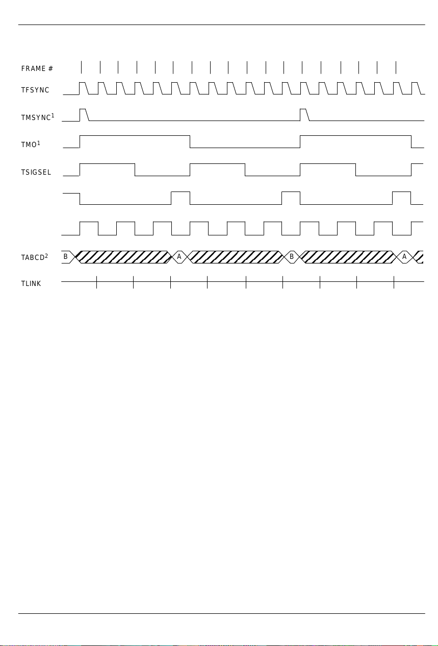
193S TRANSMIT MULTIFRAME TIMING Figure 9
DS2180A
FRAME #
TFSYNC
TMSYNC
1
TMO
TSIGSEL
TSIGFR
TLCLK
TABCD
3
TLINK
1
2
123 4567 891011121 23 45612
BABA
NOTES:
1. Transmit frame and multiframe timing may be established in one of four ways:
a. With TFSYNC tied low, TMSYNC may be pulsed high once every multiframe period to establish multiframe
boundaries, allowing internal counters to determine frame timing.
b. TFSYNC may be pulsed every 125 microseconds; pulsing TMSYNC once establishes multiframe bound-
aries.
c. TMSYNC and TFSYNC may be continuously pulsed to establish and reinforce frame and superframe tim-
ing.
d. If TMSYNC is tied low and TFSYNC is pulsed at frame boundaries, the transmitter will establish an arbi-
trary multiframe boundary as indicated by TMO.
2. Channels in which robbed bit signaling is enabled will sample TABCD during the LSB bit time in frames indi-
cated.
3. When external S-bit insertion is enabled, TLINK will be sampled during the F-bit time of even frames and in-
serted into the outgoing data stream.
041995 11/36
Page 12

DS2180A
193E TRANSMIT MULTIFRAME TIMING Figure 10
FRAME #
TFSYNC
TMSYNC
1
TMO
TSIGSEL
TSIGFR
TLCLK
TABCD
3
TLINK
1 2 3 4 5 6 7 8 91011 12131415 16171824
1
2
DABC
19 20 21 22 23 124
D
NOTES:
1. Transmit frame and multiframe timing may be established in one of four ways:
a. With TFSYNC tied low, TMSYNC may be pulsed high once every multiframe period to establish multiframe
boundaries, allowing internal counters to determine frame timing.
b. TFSYNC may be pulsed every 125 microseconds; pulsing TMSYNC once establishes multiframe bound-
aries.
c. TMSYNC and TFSYNC may be continuously pulsed to establish and reinforce frame and superframe tim-
ing.
d. If TMSYNC is tied low and TFSYNC is pulsed at frame boundaries, the transmitter will establish an arbi-
trary multiframe boundary as indicated by TMO.
2. Channels in which robbed bit signaling is enabled will sample TABCD during the LSB bit time in frames indi-
cated.
3. TLINK is sampled during the F-bit time of odd frames and inserted into the outgoing data stream (FDL data).
041995 12/36
Page 13

TRANSMIT MULTIFRAME BOUNDARY TIMING Figure 11
TCLK
TMSYNC
TMO
TFSYNC
TSIGSEL
TSIGFR
TLCLK
TCHCLK
1
TLINK
DS2180A
TABCD
2
TSER
LSB MSB LSB MSBF LSB MSB
TPOS,
TNEG
LSB MSB LSB MSB LSB MSBF
NOTES:
1. TLINK timing shown is for 193E framing; in 193E framing, TLINK is sampled as indicated for insertion into
F-bit position of odd frames. When S-bit insertion is enabled in 193S, TLINK is sampled during even frames.
2. If TCR.5=1, TSER is sampled during the F-bit time of CRC frames for insertion into the outgoing data stream
(193E framing only).
041995 13/36
Page 14

DS2180A
RECEIVE CONTROL REGISTER Figure 12
(MSB) (LSB)
ARC OOF RCI RCS SYNCC SYNCT SYNCE RESYNC
SYMBOL POSITION NAME AND DESCRIPTION
ARC RCR.7 Auto Resync Criteria.
OOF RCR.6 Out-of-frame (OOF) Condition Detection.
RCI RCR.5 Receive Code Insert. When set, the receive code selected by RCR.4 is
RCS RCR.4 Receive Code Select.
SYNCC RCR.3 Sync Criteria. Determines the type of algorithm utilized by the receive syn-
SYNCT RCR.2 Sync Time. If set, 24 consecutive F-bits of the framing pattern must be
SYNCE RCR.1 Sync Enable. If clear, the transceiver will automatically begin a resync if
RESYNC RCR.0 Resync. When toggled low to high, the transceiver will initiate resync im-
0 = Resync on OOF or RCL event.
1 = Resync on OOF only.
0 = 2 of 4 framing bits in error.
1 = 2 of 5 framing bits in error.
inserted into channels marked by RMR registers. If clear, no code is inserted.
0 = Idle code (7F Hex).
1 = Digital milliwatt.
chronizer and differs for each frame mode.
193S Framing (CCR.4=0).
0 = Synchronize to frame boundaries using F
tiframe by using F
1 = Cross couple F
193E Framing (CCR.4=1).
.
S
and FS patterns in sync algorithm.
T
pattern, then search for mul-
T
0 = Normal sync (utilizes FPS only).
1 = Validate new alignment with CRC before declaring sync.
qualified before sync is declared. If clear, 10 bits are qualified.
two of the previous four or five framing bits were in error or if carrier loss is
detected. If set, no auto resync occurs.
mediately . The bit must be cleared, then set again for subsequent resyncs.
RECEIVE CODE INSERTION
Incoming receive channels can be replaced with idle (7F
Hex) or digital milliwatt (µ-LAW format) codes. The receive mark registers indicate which channels are inserted. When set, bit RCR.5 serves as a “global” enable
for marked channels and bit RCR.4 selects inserted
code format: 0 = idle code, 1 = digital milliwatt.
041995 14/36
RECEIVE SYNCHRONIZER
Bits RCR.0 through RCR.3 allow the user to control operational characteristics of the synchronizer . Sync algorithm, candidate qualify testing, auto resync, and command resync modes may be altered at any time in
response to changing span conditions.
Page 15

DS2180A
RECEIVE SIGNALING
Robbed bit signaling data is presented at RABCD during each channel time in signaling frames for all 24 in-
coming channels. Logical combination of clocks
RMSYNC, RSIGFR and RSIGSEL allow the user to
identify and extract AB or ABCD signaling data.
RMR1–RMR3: RECEIVE MARK REGISTERS Figure 13
(MSB) (LSB)
CH8
CH7 CH6 CH5 CH4 CH3 CH2 CH1 RMR1
CH16 CH15 CH14 CH13 CH12 CH11 CH10 CH9 RMR2
CH24 CH23 CH22 CH21 CH20 CH19 CH18 CH17 RMR3
SYMBOL POSITION NAME AND DESCRIPTION
CH24 RMR3.7 Receive Mark Registers. Each of these bit positions represents a DS0
CH1 RMR1.0 channel in the incoming T1 frame. When set, the corresponding channel
will output codes determined by RCR.4 and RCR.5.
193S RECEIVE MULTIFRAME TIMING Figure 14
123
FRAME #
RFSYNC
RMSYNC
RSIGSEL
12
4
56789101112123 45
6
RSIGFR
RLCLK
1
RABCD
RLINK
BABA
2
NOTES:
1. Signaling data is updated during signaling frames on channel boundaries. RABCD is the LSB of each channel
word in non-signaling frames.
2. RLINK data (S-bit) is updated one bit time prior to S-bit frames and held for two frames.
041995 15/36
Page 16

DS2180A
193E RECEIVE MULTIFRAME TIMING Figure 15
FRAME#
RFSYNC
RMSYNC
RSIGSEL
RSIGFR
RLCLK
RABCD
2
RLINK
1 2 3 4 5 6 7 8 9 1011121314 151617
1
D
AB C
18 19 20 21 22 23 2424
D
NOTES:
1. Signaling data is updated during signaling frames on channel boundaries. RABCD outputs the LSB of each
channel word in non-signaling frames.
2. RLINK data (FDL-bit) is updated one bit time prior to odd frames and held for two frames.
041995 16/36
Page 17

RECEIVE MULTIFRAME BOUNDARY TIMING Figure 16
RCLK
2
RPOS,
RNEG
RFSYNC
RMSYNC
RSIGSEL
RSIGFR
RLCLK
RCHCLK
1
RLINK
LSB MSBLSB MSBF LSB MSB
DS2180A
RABCD
CHANNEL 24 B OR DCHANNEL 23 B OR D
RSER
LSB MSB LSB MSBF LSB MSB
NOTES:
1. RLINK timing is shown for 193E; in 193S, RLINK is updated on even frame boundaries and is held across
multiframe edges.
2. Total delay from RPOS and RNEG to RSER output is 13 RCLK periods.
041995 17/36
Page 18

DS2180A
RSR: RECEIVE STATUS REGISTER Figure 17
(MSB) (LSB)
BVCS ECS RYEL RCL FERR B8ZSD RBL RLOS
SYMBOL POSITION NAME AND DESCRIPTION
BVCS RSR.7 Bipolar Violation Count Saturation. Set when the 8-bit counter at BVCR
ECS RSR.6 Error Count Saturation. Set when either of the 4-bit counters at ECR satu-
RYEL RSR.5 Receive Yellow Alarm. Set when yellow alarm detected. (Detected yellow
RCL RSR.4 Receive Carrier Loss. Set when 32 consecutive 0’s appear at RPOS and
FERR RSR.3 Frame Bit Error. Set when FT (193S) or FPS (193E) bit error occurs.
B8ZSD RSR.2 Bipolar Eight Zero Substitution Detect. Set when B8ZS code word de-
RBL RSR.1 Receive Blue Alarm. Set when two consecutive frames have less than
RLOS RSR.0 Receive Loss of Sync. Set when resync is in process; if RCR.1=0, RLOS
saturates.
rates.
alarm format determined by CCR.4 and CCR.3.)
RNEG.
tected.
three 0’s (total) in the data stream (F-bit positions not tested).
transitions high on an OOF event or carrier loss indicating auto resync.
RECEIVE ALARM REPORTING
Incoming serial data is monitored by the transceiver for
alarm occurrences. Alarm conditions are reported in
two ways: via transitions on the alarm output pins and
registered interrupt, in which the host controller reads
the RSR in response to an alarm-driven interrupt. Interrupts may be direct, in which the transceiver demands
service for a real-time alarm, or count-overflow triggered, in which an onboard alarm event counter exceeds a user-programmed threshold. The user may
mask individual alarm conditions by clearing the appropriate bits in the receive interrupt mask register
(RIMR).
041995 18/36
ALARM SERVICING
The host controller must service the transceiver in order
to clear an interrupt condition. Clearing appropriate bits
in the RIMR will unconditionally clear an interrupt. Direct
interrupt (those driven from real-time alarms) will be
cleared when the RSR is directly read unless the alarm
condition still exists. Count-overflow interrupts (BVCS,
ECS) are not cleared by a direct read of the RSR. They
will be cleared only when the user presets the appropriate count register to a value other than all 1’s. A burst
read of the RSR will not clear an interrupt condition.
Page 19

RIMR: RECEIVE INTERRUPT MASK REGISTER Figure 18
(MSB) (LSB)
BVCS ECS RYEL RCL FERR B8ZSD RBL RLOS
SYMBOL POSITION NAME AND DESCRIPTION
BVCS RIMR.7 Bipolar Violation Count Saturation Mask.
1 = Interrupt masked.
0 = Interrupt masked.
ECS RIMR.6 Error Count Saturation Mask.
1 = Interrupt enabled.
0 = Interrupt masked.
RYEL RIMR.5 Receive Yellow Alarm Mask.
1 = Interrupt enabled.
0 = Interrupt masked.
RCL RIMR.4 Receive Carrier Loss Mask.
1 = Interrupt enabled.
0 = Interrupt masked.
FERR RIMR.3 Frame Bit Error Mask.
1 = Interrupt enabled.
0 = Interrupt masked.
B8ZSD RIMR.2 B8ZS Detect Mask.
1 = Interrupt enabled.
0 = Interrupt masked.
RBL RIMR.1 Receive Blue Alarm Mask.
1 = Interrupt enabled.
0 = Interrupt masked.
RLOS RIMR.0 Receive Loss of Sync Mask.
1 = Interrupt enabled.
0 = Interrupt masked.
DS2180A
ALARM COUNTERS
The three onboard alarm event counters allow the transceiver to monitor and record error events without processor intervention on each event occurrence. All of
these counters are presettable by the user establishing
an event count interrupt threshold. As each counter saturates, the next error event occurrence will set a bit in
the RSR and generate an interrupt unless masked. The
user may read these registers at any time; in many systems, the host will periodically poll these registers to establish link error rate performance.
OOF EVENTS AND ERRORED
SUPERFRAMES
Out of frame is declared when at least two of four (or
five) consecutive framing bits are in error. FT bits are
tested for OOF occurrence in 193S; the FPS bits are
tested in 193E. OOF events are recorded by the 4-bit
OOF counter in the error counter register. In the 193E
framing mode, the OOF event is logically OR’ed with an
on-chip generated CRC checksum. This event, known
as errored superframe, is recorded by the 4-bit ESF error counter in the error count register. In the 193S framing mode, the 4-bit ESF error counter records individual
and FS errors when RCR.3=1 or FT errors only when
F
T
RCR.3=0.
041995 19/36
Page 20

DS2180A
BVCR: BIPOLAR VIOLATION COUNT REGISTER Figure 19
(MSB) (LSB)
BVD7 BVD6 BVD5 BVD4 BVD3 BVD2 BVD1 BVD0
SYMBOL POSITION NAME AND DESCRIPTION
BVD7 BVCR.7 MSB of bipolar count.
BVD0 BVCR.0 LSB of bipolar count.
This 8-bit binary up counter saturates at 255 and will
generate an interrupt for each occurrence of a bipolar
violation once saturated (RIMR.7=1). Presetting this
register allows the user to establish specific count inter-
from the preset valued and may be read at any time.
Counter increments occur at all times and are not disabled by resync. If B8ZS is enabled (CCR.2=1) bipolar
violations are not counted for B8ZS code words.
rupt thresholds. The counter will count “up” to saturation
ECR: ERROR COUNT REGISTER Figure 20
(MSB) (LSB)
OOFD3
SYMBOL POSITION NAME AND DESCRIPTION
OOFD3 ECR.7 MSB of OOF event count.
OOFD0 ECR.4 LSB of OOF event count.
ESFD3 ECR.3 MSB of extended superframe error count.
ESFD0 ECR.0 LSB of extended superframe error count.
These separate 4-bit binary up counters saturate at a
count of 15 and will generate an interrupt for each occurrence of an OOF event or an ESF error event after saturation (RIMR.6=1). Presetting these counters allows the
user to establish specific count interrupt thresholds. The
counters will count “up” to saturation from the preset value and may be read at any time. These counters share
the same register address and must be written to or read
from simultaneously.
The OOF counter records out-of-frame events in both
193S and 193E. The ESF error counter records errored
superframes in 193E. In 193S, the ESF counter records
individual F
only when RCR.3=0. ECR counter increments are disabled when resync is in progress (RLOS high).
OOFD2 OOFD1 OOFD0 ESFD3 ESFD2 ESFD1 ESFD0
ERROR COUNT ESF ERROR COUNT
ALARM OUTPUTS
The transceiver also provides direct alarm outputs for
applications when additional decoding and demuxing
are required to supplement the onboard alarm logic.
RLOS OUTPUT
The receive loss of sync output indicates the status of
the receiver synchronizer circuitry; when high, an offline resynchronization is in progress and a high-low
transition indicates resync is complete. The RLOS bit
(RSR.0) is a “latched” version of the RLOS output. If the
auto-resync mode is selected (RCR.1=0), RLOS is a
and FS errors when RCR.3=1; FT errors
T
real time indication of a carrier loss or OOF event occurrence.
041995 20/36
Page 21

DS2180A
RYEL OUTPUT
The yellow alarm output transitions high when a yellow
alarm is detected. A high-low transition indicates the
alarm condition has been cleared. The RYEL bit
(RSR.5) is a “latched” version of the RYEL output. In
193E framing, the yellow alarm pattern detected is 16
pattern sets of 00 (Hex) and FF (Hex) received at
RLINK. In 193S, framing the yellow alarm format is dependent on CCR.3; if CCR.3=0, the RYEL output transitions high if bit 2 of 256 or more consecutive channels is
0; if CCR.3=1, yellow alarm is declared when the S-bit
received in frame 12 is 1.
RBV OUTPUT
The bipolar violation output transitions high when an accused bit emerges at RSER. RBV will go low at the next
bit time if no additional violations are detected.
ALARM OUTPUT TIMING Figure 21
RCLK
RFSYNC
RMSYNC
RFER OUTPUT
The receive frame error output transitions high at the Fbit time and is held high for two bit periods when a frame
bit error occurs. In 193S framing, FT and FS patterns are
tested. The FPS pattern is tested in 193E framing. Additionally , in 193E framing, RFER reports a CRC error by a
low-high-low transition (one bit period wide) one half
RCLK period before a low-high transition on RMSYNC.
RESET
A high-low transition on RST clears all registers and
forces immediate receive resync when RST returns
high. This reset has no effect on transmit frame multiframe or channel counters. RST must be held low on
system power-up to insure proper initialization of transceiver counters and registers. Following reset, the host
processor should restore all control modes by writing
appropriate registers with control data.
1
RFER
2
RBV
3
RCL
4
RLOS
NOTES:
1. RFER transitions high during F-bit time if received framing pattern bit is in error. (Frame 12 F-bits in 193S are
ignored if CCR.3=1). Also, in 193E, RFER transitions 1/2 bit time before the rising edge of RMSYNC to indicate
a CRC error for the previous multiframe.
2. RBV indicates received bipolar violation and transitions high when an accused bit emerges from RSER. If
B8ZS is enabled, RBV will not report the zero replacement code.
3. RCL transitions high (during 32nd bit time) when 32 consecutive bits received are 0; RCL transitions low when
the next 1 is received.
4. RLOS transitions high during the F-bit time that caused an OOF event (any two of four consecutive F
bits are in error) if auto-resync mode is selected (RCR.1=0). Resync will also occur when loss of carrier is detected (RCL=1). When RCR.1=1, RLOS remains low until resync occurs, regardless of OOF or carrier loss
flags. In this situation, resync is initiated only when RCR.0 transitions low-to-high or the RST
pin transitions
high-low-high.
or FPS
T
041995 21/36
Page 22

DS2180A
HARDWARE MODE
For preliminary system prototyping or applications
which do not require the features offered by the serial
port, the transceiver can be reconfigured by the SPS
pin. Tying SPS to V
disables the serial port, clears all
SS
internal registers except CCR and TCR and redefines
pins 14 through 18 as mode control inputs. The hardware mode allows device retrofit into existing applications where mode control and alarm conditioning hardware is often designed with discrete logic.
HARDWARE COMMON CONTROL
In the hardware mode bits TCR.2, CCR.4, TCR.0,
CCR.1 and CCR.2 map to pins 14 through 18. The loop-
HARDWARE MODE Table 6
PIN NUMBER REGISTER BIT
14 (16) TCR-D2 193S – S-bit insertion
15 (17) CCR-D4 Framing Mode Select.
16 (18) TCR-D0 Transmit Yellow Alarm
17 (19) CCR-D1 Zero Suppression
18 (20) CCR-D2 B8ZS1.
LOCATION
1 = external; 0 = internal
1 = 193E; 0 = 193S
1 = enabled; 0 = disabled
1 = bit 7 stuffing
0 = transparent
1 = enabled; 0 = disabled
back feature (bit CCR.0) is enabled by tying pins 17
(zero suppression) and 18 (B8ZS) to 1. (The last states
of pins 17 and 18 are latched as when both pins are taken high, preserving the current zero suppression
mode). Robbed bit signaling (bit TCR.4) is enabled for
all channels. The user may tie TSER to TABCD externally to disable signaling if so desired. Bit CCR.3 is
forced to 0 which selects bit 2 yellow alarm in 193S framing. Contents of the RCR, as well as the remaining bit
locations in the CCR and TCR are cleared in the hardware mode. The RST input may be used to force immediate receiver resync and has no effect on transmit.
NAME AND DESCRIPTION
3
2 ,3
1
NOTES:
1. Tying pins 17 and 18 high enables loopback in the hardware mode.
2. Bit 2 (193S) and data link (193E) yellow alarms are supported.
3. S-bit yellow alarm (193S) is not internally supported; however, the user may elect to insert external S bits for
alarm purposes.
4. Pin numbers for PLCC package are listed in parenthesis.
041995 22/36
Page 23

T1 OVERVIEW
DS2180A
Framing Standards
The DS2180A is compatible with the existing Bell System D4 framing standard described in ATT PUB 43801
and the new extended superframe format (ESF) as described in ATT C.B. #142. In this document, D4 framing
is referred to as 193S and ESF (also known as Fe) is referred to as 193E. Programmable features of the
DS2180A allow support of other framing standards
which are derivatives of 193E and 193S. The salient differences between the 193S and 193E formats are the
number of frames per superframe and use of the F-bit
position. In 193S, 12 frames make up a superframe, in
193E, 24. A frame consists of 24 channels (timeslots) of
8-bit data preceded by an F-bit. Channel data is transmitted and received MSB first.
F-Bits
The use of the F-bit position in 193S is split between the
terminal framing pattern (know as FT-bits) which provides frame alignment information and the signaling
framing pattern (known as F
tiframe alignment information. In 193E framing, the F-bit
position is shared by the framing pattern sequence
-bits) which provides mul-
S
(FPS) which provides frame and multiframe alignment
information, a 4 KHz data link known as FDL (Facility
Data Link), and CRC (Cyclic Redundancy Check) bits.
The FDL bits are used for control and maintenance (inserted by the user at TLINK) and the CRC bits are an indicator of link quality and may be monitored by the user
to establish error performance.
Signaling
During frames 6 and 12 in 193S, A and B signaling information is inserted into the LSB of all channels transmitted. In 193E, A and B data is inserted into frames 6
and 12 and C and D data is inserted into frames 18 and
24. This allows a maximum of four signaling states to be
transmitted per superframe in 193S and 16 states in
193E.
Alarms
The DS2180A supports all alarm pattern generation and
detection required in typical Bell System applications.
These alarm modes are explained in ATT PUB 43801,
ATT C.B. #142 and elsewhere in this document.
041995 23/36
Page 24

DS2180A
193E FRAMING FORMAT Table 7
FRAME
NUMBER
1
2
3
4
5
6
7
8
9
10
11
12
13
14
15
16
17
18
19
20
21
22
23
24
F-BIT USE BIT USE IN EACH CHANNEL SIGNALING-BIT USE
FPS1FDL2CRC
–
–
–
0
–
–
–
0
–
–
–
1
–
–
–
0
–
–
–
1
–
–
–
1
M
–
C1
M
–
M
–
C2
M
–
M
–
C3
M
–
M
–
C4
M
–
M
–
C5
M
–
M
–
C6
M
–
3
DATA SIGNALING 2
STATE4STATE16STATE
–
BITS 1–8
BITS 1–8
–
BITS 1–8
–
BITS 1–8
–
BITS 1–8
BITS 1–7
–
BITS 1–8
–
BITS 1–8
–
BITS 1–8
BIT 8
A
A
A
BITS 1–8
–
BITS 1–8
–
BITS 1–7
–
BITS 1–8
BIT 8
A
B
B
BITS 1–8
–
BITS 1–8
–
BITS 1–8
–
BITS 1–8
BITS 1–7
–
BITS 1–8
–
BITS 1–8
–
BITS 1–8
BIT 8
A
A
C
BITS 1–8
–
BITS 1–8
–
BITS 1–7
BIT 8
A
B
D
NOTES:
1. FPS – Framing Pattern Sequence.
2. FDL – 4 KHz Facility Data Link; M = message bits.
3. CRC – Cyclic Redundancy Check bits. The CRC code will be internally generated by the device when
TCR.5=0. When TCR.5=1, externally supplied CRC data will be sampled at TSER during the F-bit time of
frames 2, 6, 10, 14, 18, 22.
4. The user may program any individual channels clear, in which case bit 8 will be used for data, not signaling.
5. Depending on application, the user can support 2-state, 4-state or 16-state signaling by the appropriate decodes of TMO, TSIGFR, TSIGSEL (Transmit Side) and RMSYNC, RSIGFR and RSIGSEL (Receive Side).
041995 24/36
Page 25

DS2180A
193S FRAMING FORMAT Table 8
FRAME
NUMBER
1
2
3
4
5
6
7
8
9
10
11
12
F-BIT USE BIT USE IN EACH CHANNEL
1
F
T
1
–
0
–
1
–
0
–
1
–
0
–
2
F
S
–
0
–
0
–
1
–
1
–
1
–
3
0
DATA SIGNALING
BITS 1–8
BITS 1–8
BITS 1–8
BITS 1–8
BITS 1–8
BITS 1–7
BIT 8
BITS 1–8
BITS 1–8
BITS 1–8
BITS 1–8
BITS 1–8
BITS 1–7
BIT 8
4
SIGNALING-BIT USE
A
B
NOTES:
1. FT (terminal framing) bits provide frame alignment information.
(signaling frame) bits provide multiframe alignment information.
2. F
S
3. The S-bit in frame 12 may be used for yellow alarm transmission and detection in some applications.
4. The user may program any individual channels clear, in which case bit 8 will be used for data, not signaling.
Line Coding
T1 line data is transmitted in a bipolar alternative mark
inversion line format; 1’s are transmitted as alternating
negative and positive pulses and 0’s are simply the absence of pulses. This technique minimizes DC voltage
on the T1 span and allows clock to be extracted from
data. The network currently has a 1’s density constraint
to keep clock extraction circuitry functioning which is
usually met by forcing bit 7 of any channel consisting of
all 0’s to 1. The use of Bipolar Eight Zero Substitution
(B8ZS) satisfies all the 1’s density requirement while allowing data traffic to be transmitted without corruption.
This feature is known as clear channel and is explained
more completely in ATT C.B. #144. When the B8ZS fea-
ture is enabled, any outgoing stream of eight consecutive 0’s is replaced with a B8ZS code word. If the last 1
transmitted was positive, the inserted code is 000+-0-+;
if negative, the code word inserted is 000-+0+-. Bipolar
violations occur in the fourth and seventh bit positions
which are ignored by the DS2180A error monitoring logic when B8ZS is enabled. Any received B8ZS code word
is replaced with all 0’s if B8ZS is enabled. Also, the receive status register will report any occurrence of B8ZS
code words to the host controller. This allows the user to
monitor the link for upgrade to clear channel capability
and respond to it. The B8ZS monitoring feature works at
all times and is independent of the state of CCR.2.
041995 25/36
Page 26

DS2180A
TRANSMIT SIDE OVERVIEW
The transmit side of the DS2180A is made up of six major functional blocks: timing and clock generation, data
selector, bipolar coder, yellow alarm, F-bit data and
CRC. The timing and clock generation circuit develops
all onboard and output clocks to the system from inputs
TCLK, TFSYNC, and TMSYNC. The yellow alarm circuitry generates mode–dependent yellow alarms. The
CRC block generates checksum results utilized in 193E
framing. F-bit data provides mode–dependent framing
patterns and allows insertion of link or S-bit data externally. All of these blocks feed into the data selector
where, under control of the CCR, TCR, TIRs and TTRs,
the contents of the outgoing data stream are established by bit selection and insertion. The bipolar coder
formats the output of the data selector to make it compatible with bipolar transmission techniques and inserts
zero suppression codes. The bipolar coder also supports the onboard loopback feature. Input-to-output
delay of the transmitter is 10 TCLK cycles.
Resync (RCR.0)
A zero-to-one transition of RCR.0 causes the synchronizer to search for the framing pattern sequence immediately, regardless of the internal sync status. In order to initiate another resync command, this bit must be
cleared and then set again.
Sync Enable (RCR.1)
When RCR.1 is cleared, the receiver will initiate automatic resync if any of the following events occur: 1) an
OOF event (“out-of-frame”), or 2) carrier loss (32 consecutive 0’s appear at RPOS and RNEG). An OOF
event occurs any time that 2 of 4 F
error. When RCR.1 is set, the automatic resync circuitry
is disabled; in this case, resync can only be initiated by
setting RCR.0 to 1 or externally via a low-high transition
. Note that using RST to initiate resync resets the
on RST
receive output timing while RST is low; use of RCR.1
does not affect output timing until the new alignment is
located.
or FPS bits are in
T
RECEIVE SIDE OVERVIEW
Synchronizer
The heart of the receiver is the synchronizer monitor.
This circuit serves two purposes: 1) monitoring the incoming data stream for loss of frame or multiframe
alignment, and 2) searching for new frame alignment
pattern when sync loss is detected. When sync loss is
detected, the synchronizer begins an off-line search for
the new alignment; all output timing signals remain at
the old alignment with the exception of RSIGFR which is
forced low during resync. When one and only one candidate is qualified, the output timing will move to the new
alignment at the beginning of the next multiframe. One
frame later, RLOS will transition low, indicating valid
sync and the resumption of the normal sync monitoring
mode. Several bits in the RCR allow tailoring of the resync algorithm by the user. These bits are described below.
Sync Time (RCR.2)
Bit RCR.2 determines the number of consecutive framing pattern bits to be qualified before SYNC is declared.
If RCR.2=1, the algorithm will validate 24 bits; if
RCR.2=0, 10 bits are validated. 24-bit testing results in
superior false framing protection, while 10-bit testing
minimizes reframe time (although in either case, the
synchronizer will only establish resync when one and
only one candidate is found).
Sync Criteria (RCR.3)
193E
Bit RCR.3 determines which sync algorithm is utilized
when resync is in progress (RLOS=1). In 193E framing,
when RCR.3=0, the synchronizer will lock only to the
FPS pattern and will move to the new frame and multiframe alignment after the move to the new alignment.
When RCR.3=1, the new alignment is further tested by a
CRC code match. RLOS will transition low after a CRC
match occurs. If no CRC match occurs in three attempts
(three multiframes), the algorithm will reset and a new
search for the framing pattern begins. It takes 9 ms for
the synchronizer to check the first CRC code after the
new alignment has been loaded. Each additional CRC
test takes 3 ms. Regardless of the state of RCR.3, if
more than one candidate exists after about 24 ms, the
synchronizer will begin eliminating emulators by testing
their CRC codes online in order to find the true framing
candidate.
193S
In 193S framing, when RCR.3=1, the synchronizer will
cross check the FT pattern with the FS pattern to help
eliminate false framing candidates such as digital milliwatts. The FS patterns are compared to the
repeating pattern ...00111000111000...(00111X0 if
CCR.3–YELMD–is equal to a 1). In this mode, F
FS patterns must be correctly identified by the synchro-
T
and
041995 26/36
Page 27

DS2180A
nizer before sync is declared. Clearing RCR.3 causes
the synchronizer to search for F
without cross-coupling the F
be established using the F
patterns (101010...)
T
pattern. Frame sync will
S
information, while multi-
T
frame sync will be established only if valid FS information is present. If no valid FS pattern is identified, the synchronizer will move to the F
alignment, RLOS will go
T
low, and a false multiframe position may be indicated by
RMSYNC. RFER will indicate when the received S-bit
pattern does not match the assumed internal multiframe
alignment. This mode will be used in applications where
non-standard S-bit patterns exist. In such applications,
multiframe alignment information can be decoded externally by using the S-bits present at RLINK.
AVERAGE REFRAME TIME1 Table 9
FRAME MODE
MIN AVG MAX MIN AVG MAX
193S 3.0 3.75 4.5 6.5 7.25 8.0
193E 6.0 7.5 9.0 13.0 14.5 16.0
RCR.2=0 RCR.2=1
UNITS
ms
NOTE:
1. Average Reframe Time is defined here as the average time it takes from the start of sync (rising edge of
RLOS) to the actual loading of the new alignment (on a multiframe edge) into the output receive timing.
041995 27/36
Page 28

DS2180A
BACKPLANE INTERFACE USING DS2180A AND DS2176 Figure 22
TRANSMIT
LINE INTERFACE
DS2186
RECEIVE
LINE INTERFACE
DS2187
TPOS
TNEG
RPOS
RNEG
TSIGSEL
TSIGFR
TCHCLK
TABCD
TSER
TCLK
TMO
TFSYNC
TRANSMIT
BACKPLANE
INTERFACE
SIGNALING
PCM
CONTROL
DATA LINK
SUPERVISION
VDD
SPS
RLCLK
TLCLK
RLINK
TLINK
TMSYNC
TEST
VSS
DS2180A
RCLK
RMSYNC
RSER
RFER
RLOS
INT
RST
SDI
SCLK
CS
SDO
HOST
CONTROLLER
RCLK
RMSYNC
RSER
SMO
SIGH
SM1
SLIP
FMS
ALN
SCLKSEL
VSS
DS2176
VDD
S/P
SSER
SYSCLK
SFSYNC
SMSYNC
A
B
C
D
1.544 MHz SERIAL BACKPLANE
041995 28/36
Page 29

PROCESSOR-BASED TRANSMIT SIGNALING INSERTION Figure 23
8031/51 DS2180A
12
INT0
10
RXD
11
TXD
1
P1.0
P1.1
INT1
2
13
3
SI
4
D0
5
6
7
D1
D2
D3
CY7C401
(64 x 4 FIFO)
MR
SO
Q0
Q1
Q2
Q3
15
13
12
11
10
19
14
16
15
18
17
8
4
9
1
2
SPS
INT
SDO
SDI
SCLK
CS
TSIGFR
TCHCLK
TABCD
TMSYNC
TFSYNC
DS2180A
TPOS
TNEG
Multiframe Sync
PROCESSOR-BASED SIGNALING
Many robbed-bit signaling applications utilize a microprocessor to insert transmit signaling data into the outgoing data stream. The circuit shown in Figure 23 “decouples” the processor timing from that of the DS2180A
by use of a small FIFO memory. The processor writes to
the FIFO (six bytes are written: three for A data, three for
B data) only when signaling updates are required. The
system is interrupt-driven from the transmit multiframe
sync input; the processor must update the FIFO prior to
Frame 6 (625 µs after interrupt) to prevent data corruption. The application circuit shown supports 193S framing. Additional hardware is required for 193E applications.
041995 29/36
Page 30

DS2180A
ABSOLUTE MAXIMUM RATINGS*
Voltage on Any Pin Relative to Ground –1.0V to 7.0V
Operating Temperature 0°C to +70°C
Storage Temperature –55°C to 125°C
Soldering Temperature 260°C for 10 seconds
* This is a stress rating only and functional operation of the device at these or any other conditions above
those indicated in the operation sections of this specification is not implied. Exposure to absolute maximum rating conditions for extended periods of time may affect reliability.
RECOMMENDED DC OPERATING CONDITIONS (0°C to 70°C)
PARAMETER SYMBOL MIN TYP MAX UNITS NOTES
Logic 1 V
Logic 0 V
Supply V
IH
IL
DD
2.0 VDD + .3 V
-0.3 +0.8 V
4.5 5.0 5.5 V
CAPACITANCE (t
= 25°C)
A
PARAMETER SYMBOL MIN TYP MAX UNITS NOTES
Input Capacitance C
Output Capacitance C
IN
OUT
5 pF
7 pF
DC ELECTRICAL CHARACTERISTICS (0°C to 70°C; VDD = 5V + 10%)
PARAMETER SYMBOL MIN TYP MAX UNITS NOTES
Supply Current I
Input Leakage I
Output Leakage I
Output Current @ 2.4V I
Output Current @ .4V I
DD
LO
OH
OL
IL
-1 mA 4
+4 mA 5
3 10 mA 1,2
1 µA
1 µA 3
NOTES:
1. TCLK = RCLK = 1.544 MHz.
2. Outputs open.
3. Applies to SDO when tri-stated.
4. All outputs except INT
5. All outputs.
, which is open collector.
041995 30/36
Page 31

DS2180A
ÉÉÉ
AC ELECTRICAL CHARACTERISTICS (0°C to 70°C; VDD = 5V + 10%)
PARAMETER SYMBOL MIN TYP MAX UNITS NOTES
SDI to SCLK Setup t
SCLK to SDI Hold t
SDI to SCLK Falling Edge t
DC
CDH
CD
SCLK Low Time t
SCLK High Time t
CH
SCLK Rise & Fall Time tR, t
CS to SCLK Setup t
SCLK to CS Hold t
CS Inactive Time t
SCLK to SDO Valid
2
CS to SDO High Z t
SCLK Setup to CS Falling t
CC
CCH
CWH
t
CDV
CDZ
SCC
CL
F
50 ns
50 ns
50 ns
250 ns
250 ns
500 ns
50 ns
50 ns
250 ns
200 ns
75 ns
50 ns
NOTES:
1. Measured at VIH=2.0 V; VIL=.8 V and 10 ns maximum rise and fall time.
2. Output load capacitance = 100 pF.
SERIAL PORT WRITE AC TIMING DIAGRAM
t
CC
CS
SCLK
SDI
t
SCC
t
DC
LSB
t
CH
t
CDH
CONTROL BYTE DATA BYTE
t
t
F
R
t
CL
t
CD
LSB
t
1
CDH
NOTES:
1. Data byte bits must be valid across low clock periods to prevent transients in operating modes.
2. Shaded regions indicate ”don’t care” states of input data.
t
CCH
MSB
t
CWH
041995 31/36
Page 32

DS2180A
SERIAL PORT READ AC TIMING
CS
SCLK
t
CDV
t
CDZ
SDO
High Z
NOTE:
1. Serial port write must precede a port read to provide address information.
AC ELECTRICAL CHARACTERISTICS1 – TRANSMIT (0°C to 70°C; VDD = 5V + 10%)
PARAMETER SYMBOL MIN TYP MAX UNITS NOTES
TCLK Period t
TCLK Pulse Width tWL, t
TCLK, RCLK Rise & Fall Times tF, t
TSER, TABCD, TLINK Setup to
TCLK Falling
TSER, TABCD, TLINK Hold from
TCLK Falling
TFSYNC, TMSYNC Setup to
TCLK Rising
Propagation Delay TFSYNC to
TMO, TSIGSEL, TSIGFR, TLCLK
Propagation Delay TCLK to
TCHCLK
TFSYNC, TMSYNC Pulse Width t
t
STD
t
HTD
t
STS
t
PTS
t
PTCH
TSP
P
WH
R
250 648 ns
125 324 ns
20 ns
50 ns
50 ns
-125 125 ns
75 ns
75 ns
100 ns
NOTES:
1. Measured at VIH = 2.0V; VIL = .8V and 10 ns maximum rise and fall time.
2. Output load capacitance = 100 pF.
041995 32/36
Page 33

DS2180A
AC ELECTRICAL CHARACTERISTICS1 – RECEIVE (0°C to 70°C; VDD = 5V + 10%)
PARAMETER SYMBOL MIN TYP MAX UNITS NOTES
Propagation Delay RCLK to
RMSYNC, RFSYNC, RSIGSEL,
t
PRS
75 ns
RSIGFR, RLCLK, RCHCLK
Propagation Delay RCLK to
RSER, RABCD, RLINK
Transition Time All Outputs t
RCLK Period t
RCLK Pulse Width tWL, t
RCLK Rise & Fall Times tR, t
RPOS, RNEG Setup to RCLK
Falling
RPOS, RNEG Hold to RCLK Fal-
ling
Propagation Delay RCLK to
RYEL, RCL, RFER, RLOS, RBV
Minimum RST Pulse Width on
System Power Up or Restart
t
PRD
TTR
t
SRD
t
HRD
t
PRA
t
RST
75 ns
20 ns
P
WH
F
250 648 ns
125 324 ns
20 ns
50 ns
50 ns
75 ns
1 µs
NOTES:
1. Measured at VIH = 2.0V; VIL = .8V and 10 ns maximum rise and fall times.
2. Output load capacitance = 100 pF.
041995 33/36
Page 34

DS2180A
TRANSMIT AC TIMING DIAGRAM
TCLK
t
t
HTD
STS
TSER, TABCD,
TLINK
t
STD
TFSYNC, TMSYNC
TMO, TLCLK,
TSIGSEL, TSIGFR
TCHCLK, TPOS,
TNEG
RECEIVE AC TIMING DIAGRAM
t
PTCH
t
PTS
t
TSP
t
P
t
WH
t
WL
t
P
t
WH
t
F
t
WL
tFt
t
R
R
RCLK
RSER, RABCD,
RLINK
RMSYNC,RFSYNC,
RSIGSEL, RSIGFR,
RLCLK, RCHCLK
RYEL, RCL, RBV,
RFER, RLOS
RST
RPOS, RNEG
041995 34/36
t
PRD
t
t
t
PRS
PRA
RST
t
SRDtHRD
Page 35

DS2180A SERIAL T1 TRANSCEIVER (600 MIL DIP)
B
D
DS2180A
1
KG H
INCHES
DIM. MIN. MAX.
A 2.050 2.075
B 0.530 0.550
C 0.140 0.160
D 0.600 0.625
E 0.015 0.040
F 0.120 0.145
G 0.090 0.110
H 0.625 0.675
J 0.008 0.012
K 0.015 0.022
A
E
C
F
J
041995 35/36
Page 36

DS2180A
DS2180AQ SERIAL T1 TRANSCEIVER (PLCC)
E
E1
B
N
1
.075 MAX
D1
NOTE 1
CH1
.150
MAX
e1
E2
NOTE1: PIN 1 IDENTIFIER TO BE LOCATED IN ZONE INDICATED.
INCHES
DIM. MIN. MAX.
A 0.165 0.180
A1 0.090 0.120
A2 0.020 –
B 0.026 0.033
B1 0.013 0.021
C 0.009 0.012
CH1 0.042 0.048
D 0.685 0.695
D1 0.650 0.656
D2 0.590 0.630
E 0.685 0.695
E1 0.650 0.656
E2 0.590 0.630
e1 0.050 BSC
N 44 –
D
D2
B1
A
C
A1A2
041995 36/36
 Loading...