

Page 1
DS2172
DS2172
Bit Error Rate Tester (BERT)
FEATURES
• Generates/Detects digital bit patterns for analyzing,
evaluating and troubleshooting digital communications systems
• Operates at speeds from DC to 52 MHz
• Programmable polynomial length and feedback taps
for generation of any other pseudorandom pattern up
to 32 bits in length including: 26–1, 29–1, 211–1,
15
2
–1, 220–1, 223–1, and 232–1
• Programmable user–defined pattern and length for
generation of any repetitive pattern up to 32 bits in
length
• Large 32–bit error count and bit count registers
• Software programmable bit error insertion
• Fully independent transmit and receive sections
• 8–bit parallel control port
• Detects test patterns with bit error rates up to 10
DESCRIPTION
The DS2172 Bit Error Rate T ester (BERT) is a software
programmable test pattern generator, receiver, and
analyzer capable of meeting the most stringent error
performance requirements of digital transmission facilities. Two categories of test pattern generation (Pseudorandom and Repetitive) conform to CCITT/ITU O.151,
O.152, O.153, and O.161 standards. The DS2172
operates at clock rates ranging from DC to 52 MHz. This
wide range of operating frequency allows the DS2172 to
be used in existing and future test equipment, transmission facilities, switching equipment, multiplexers,
DACs, Routers, Bridges, CSUs, DSUs, and CPE equipment.
The DS2172 user programmable pattern registers provide the unique ability to generate loopback patterns
required for T1, Fractional–T1, Smart Jack, and other
–2
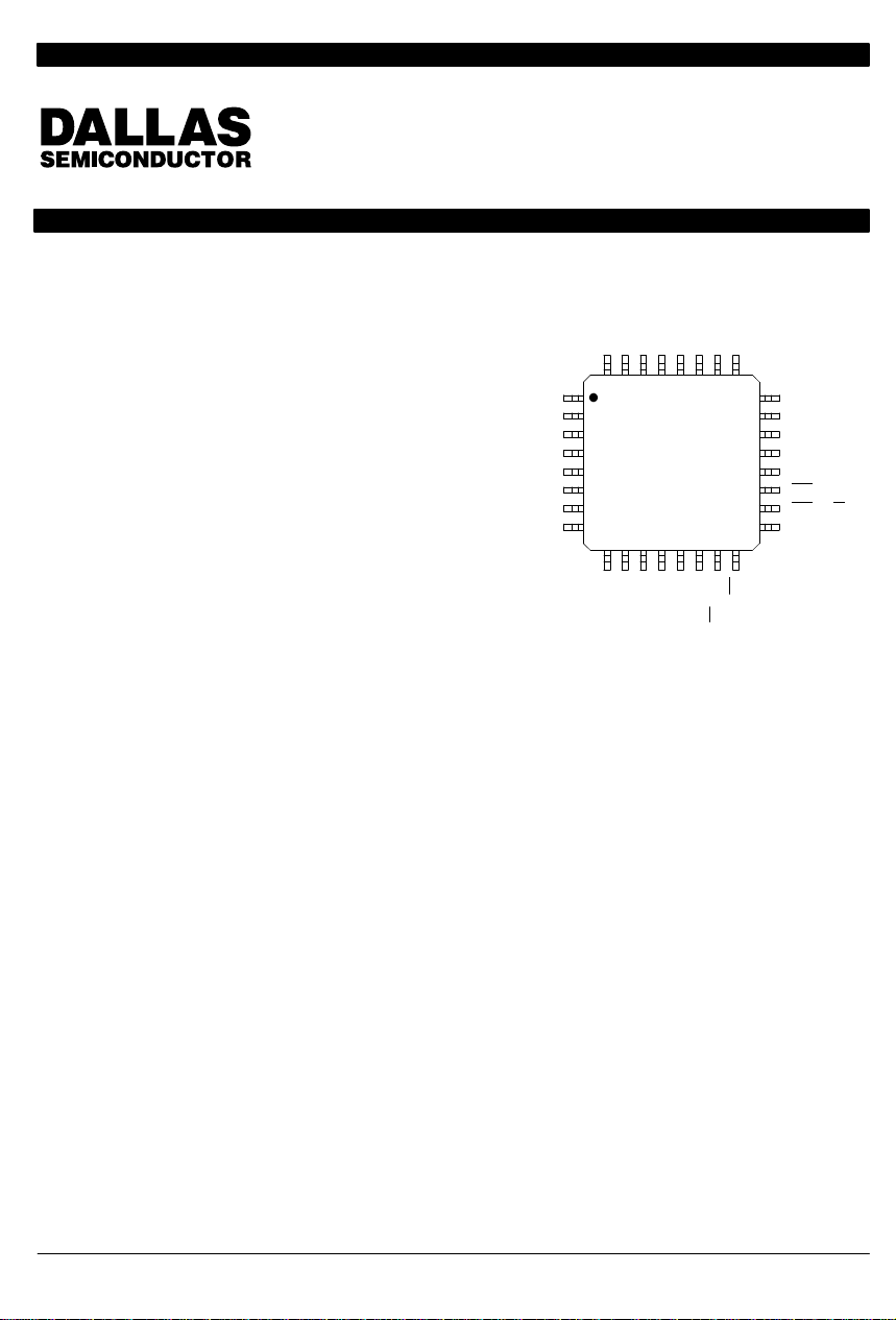
PIN ASSIGNMENT
TDATA
TDIS
TCLK
VSS
VDD
RCLK
RDIS
RDATA
32 31 30 29 28 27 26 25
TL
AD0
AD1
TEST
VSS
AD2
AD3
AD4
1
2
3
4
DS2172
32–PIN TQFP
5
6
7
8
9 101112131415 16
AD5
AD6
AD7
BTS
VSS
VDD
RD (DS)
test procedures. Hence the DS2172 can initiate the
loopback, run the test, check for errors, and finally deactivate the loopback.
The DS2172 consists of four functional blocks: the pattern generator, pattern detector , error counter , and control interface. The DS2172 can be programmed to generate any pseudorandom pattern with length up to 2
bits (See T able 5, Note 9) or any user programmable bit
pattern from 1 to 32 bits in length. Logic inputs can be
used to configure the DS2172 for applications requiring
gap clocking such as Fractional–T1, Switched–56,
DDS, normal framing requirements, and per–channel
test procedures. In addition, the DS2172 can insert
single or 10
–1
to 10–7 bit errors to verify equipment
operation and connectivity .
RL
24
23
RLOS
LC
22
21
VSS
20
VDD
19
INT
WR (R/W)
18
17
ALE (AS)
CS
32–1
Copyright 1997 by Dallas Semiconductor Corporation.
All Rights Reserved. For important information regarding
patents and other intellectual property rights, please refer to
Dallas Semiconductor data books.
031197 1/20
Page 2

DS2172
1.0 GENERAL OPERATION
1.1 Pattern Generation
The DS2172 is programmed to generate a particular
test pattern by programming the following registers:
– Pattern Set Registers (PSR)
– Pattern Length Register (PLR)
– Polynomial Tap Register (PTR)
– Pattern Control Register (PCR)
– Error Insertion Register (EIR)
Please see Tables 4 and 5 for examples of how to program these registers in order to generate some standard test patterns. Once these registers are programmed, the user will then toggle the TL (Transmit
Load) bit or pin to load the pattern into the onboard pattern generation circuitry and the pattern will begin
appearing at the TDATA pin.
1.2 Pattern Synchronization
The DS2172 expects to receive the same pattern that it
transmitted. The synchronizer examines the data at
RDATA and looks for characteristics of the transmitted
pattern. The user can control the onboard synchronizer
with the Sync Enable and Resync bits in the Pattern
Control Register.
In pseudorandom mode, the received pattern is tested
to see if it fits the polynomial generator as defined in the
transmit side. For pseudorandom patterns, only the
original pattern and an all ones pattern or an all zeros
pattern will satisfy this test. Synchronization in pseudorandom pattern mode should be qualified by using the
RA1 and RA0 indicators in the Status Register. Once in
synchronization (SR0. = 1) any deviation from this pattern will be counted by the Bit Error Count Register.
In repetitive pattern mode a received pattern of the
same length as being transmitted will satisfy this test.
Synchronization in repetitive pattern mode should be
qualified by using the RA1 and RA0 indicators in the
Status Register and examining the Pattern Receive
Register (PRR0––3). See section 10 for an explanation
of the Pattern Receive Register. Once in synchronization (SR.0 = 1) any deviation from this pattern will be
counted by the Bit Error Count Register.
1.3 BER Calculation
Users can calculate the actual Bit Error Rate (BER) of
the digital communications channel by reading the bit
error count out of the Bit Error Count Register (BECR)
and reading the bit count out of the Bit Count Register
(BCR) and then dividing the BECR value with the BCR
value. The user has total control over the integration
period of the measurement. The LC (Load Count) bit or
pin is used to set the integration period.
1.4 Generating Errors
Via the Error Insertion Register (EIR), the user can
intentionally inject a particular error rate into the transmitted data stream. Injecting errors allows users to
stress communication links and to check the functionality of error monitoring equipment along the path.
1.5 Power–Up Sequence
On power–up, the registers in the DS2172 will be in a
random state. The user must program all the internal
registers to a known state before proper operation can
be insured.
031197 2/20
Page 3
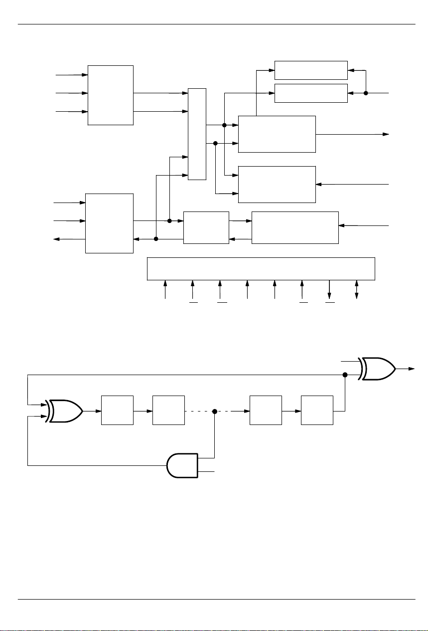
DS2172 FUNCTIONAL BLOCK DIAGRAM Figure 1
DS2172
RDIS
RCLK
RDATA
TDIS
TCLK
TDATA
RECEIVE
RATE
CONTROL
TRANSMIT
RATE
CONTROL
DETECTOR
LOOPBACK MUX
RECEIVE PATTERN
REGISTERS
ERROR
INSERTION
PARALLEL CONTROL PORT
BTS RD WR TEST ALE CS INT AD0–AD7
DS2172 PATTERN GENERATION BLOCK DIAGRAM Figure 2
TAP A FEEDBACK
BIT ERROR COUNTER
BIT COUNTER
PATTERN
PATTERN
GENERATOR
LC
SYNC
RL
TL
EIR.5
XOR
XOR DFF DFF DFF DFF
0 1 N–2 N–1
TAP B FEEDBACK
PCR.5
NOTES:
1. Tap A always equals length (N–1) of pseudorandom or repetitive pattern.
2. Tab B can be programmed to any feedback tap for pseudorandom pattern generation.
031197 3/20
Page 4
DS2172
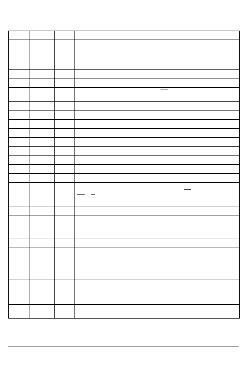
DETAILED PIN DESCRIPTION Table 1
PIN SYMBOL TYPE DESCRIPTION
1 TL I Transmit Load. A positive–going edge loads the pattern generator with the
2 AD0 I/O Data Bus. A 8–bit multiplexed address/data bus.
3 AD1 I/O Data Bus. A 8–bit multiplexed address/data bus.
4 TEST I Test. Set high to 3–state all output pins (INT, ADx, TDATA, RLOS). Should
5 V
SS
6 AD2 I/O Data Bus. A 8–bit multiplexed address/data bus.
7 AD3 I/O Data Bus. A 8–bit multiplexed address/data bus.
8 AD4 I/O Data Bus. A 8–bit multiplexed address/data bus.
9 AD5 I/O Data Bus. A 8–bit multiplexed address/data bus.
10 AD6 I/O Data Bus. A 8–bit multiplexed address/data bus.
11 AD7 I/O Data Bus. A 8–bit multiplexed address/data bus.
12 V
13 V
SS
DD
14 BTS I Bus Type Select. Strap high to select Motorola bus timing; strap low to select
15 RD (DS) I Read Input (Data Strobe).
16 CS I Chip Select. Must be low to read or write the port.
17 ALE (AS) I Address Latch Enable (Address Strobe). A positive going edge serves to
18 WR (R/W) I Write Input (Read/Write).
19 INT O Alarm Interrupt. Flags host controller during conditions defined in Status
20 V
21 V
DD
SS
22 LC I Load Count. A positive–going edge latches the current bit and bit error count
23 RLOS O Receive Loss Of Sync. Indicates the real time status of the receive synchro-
contents of the Pattern Set Registers. The MSB of the repetitive or pseudorandom pattern appears at TDATA after the third positive edge of TCLK from
asserting TL. TL is logically OR’ed with PCR.7 and should be tied to V
not used. See Figure 8 for timing information.
be tied to V
to enable all outputs.
SS
– Signal Ground. 0.0 volts. Should be tied to local ground plane.
– Signal Ground. 0.0 volts. Should be tied to local ground plane.
– Positive Supply. 5.0 volts.
Intel bus timing. This pin controls the function of the RD
(R/W) pins. If BTS = 1, then these pins assume the function listed in
WR
(DS), ALE(AS), and
parenthesis ().
demultiplex the bus.
Register. Active low, open drain output.
– Positive Supply. 5.0 volts.
– Signal Ground. 0.0 volts. Should be tied to local ground plane.
into the user accessible BCR and BECR registers and clears the internal
count registers. LC is logically OR’ed with control bit PCR.4. Should be tied
if not used.
to V
SS
nizer. Active high output; transitions low after receiving 32 matching bits.
SS
if
031197 4/20
Page 5

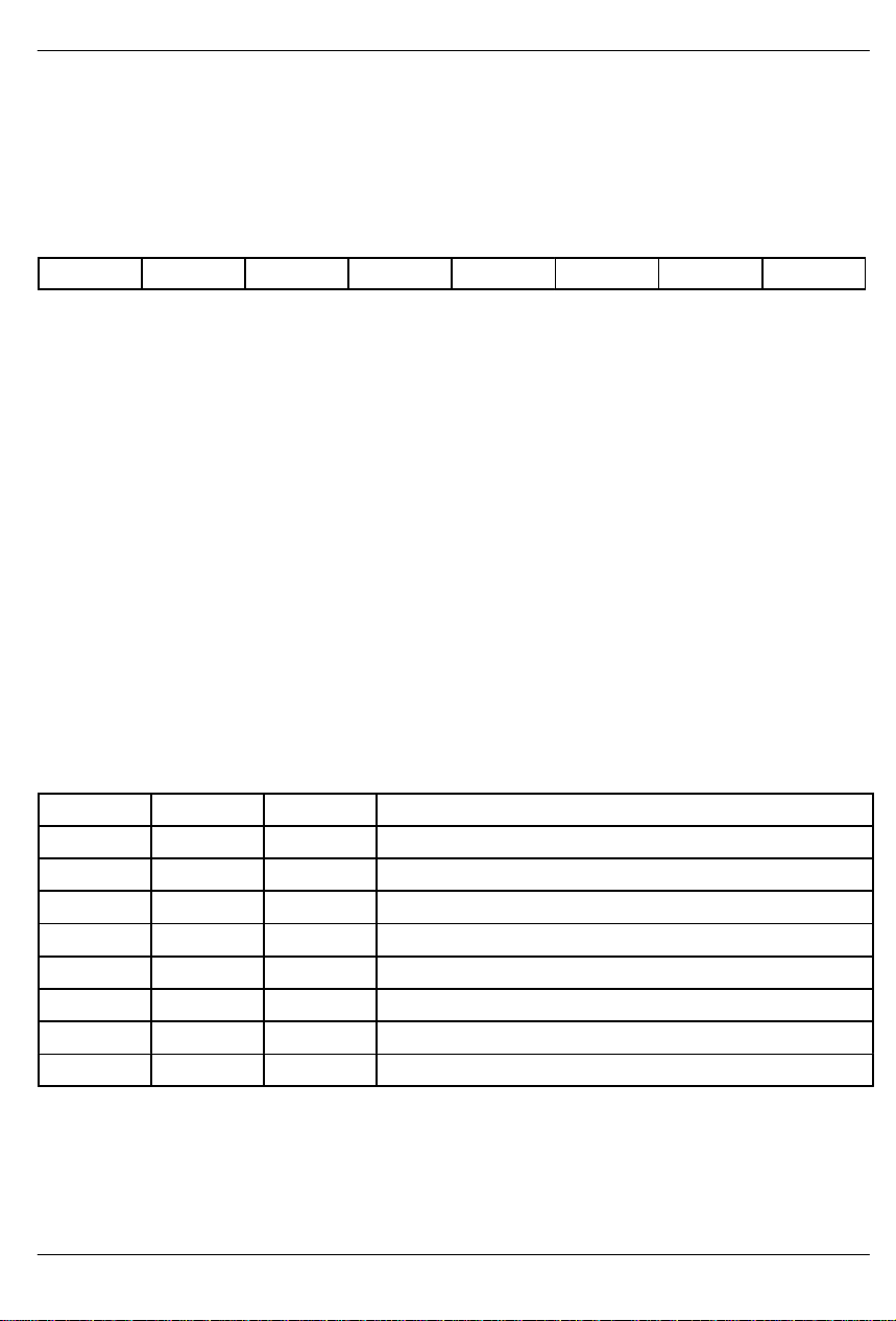
PIN DESCRIPTIONTYPESYMBOL
24 RL I Receive Load. A positive–going edge loads the previous 32 bits of data
received at RDATA into the Pattern Receive Registers. RL is logically OR’ed
with control bit PCR.3. Should be tied to V
if not used.
SS
25 RDATA I Receive Data. Received NRZ serial data, sampled on the rising edge of
RCLK.
26 RDIS I Receive Disable. Set high to prevent the data at RDATA from being
sampled. Set low to allow bits at RDATA to be sampled. Should be tied to V
if not used. See Figure 6 for timing information. All receive side operations
are disabled when RDIS is high.
27 RCLK I Receive Clock. Input clock from transmission link. 0 to 52 MHz. Can be a
gapped clock. Fully independent from TCLK.
28 V
29 V
DD
SS
– Positive Supply. 5.0 volts.
– Signal Ground. 0.0 volts. Should be tied to local ground plane.
30 TCLK I Transmit Clock. Transmit demand clock. 0 to 52 MHz. Can be a gapped
clock. Fully independent of RCLK.
31 TDIS I Transmit Disable. Set high to hold the current bit being transmitted at
TDATA. Set low to allow the next bit to appear at TDATA. Should be tied to
if not used. See Figure 7 for timing information. All transmit side opera-
V
SS
tions are disabled when TDIS is high.
32 TDATA O Transmit Data. Transmit NRZ serial data, updated on the rising edge of
TCLK.
DS2172
SS
031197 5/20
Page 6

DS2172
DS2172 REGISTER MAP Table 2
ADDRESS R/W REGISTER NAME
00 R/W Pattern Set Register 3.
01 R/W Pattern Set Register 2.
02 R/W Pattern Set Register 1.
03 R/W Pattern Set Register 0.
04 R/W Pattern Length Register.
05 R/W Polynomial Tap Register.
06 R/W Pattern Control Register.
07 R/W Error Insert Register.
08 R Bit Counter Register 3.
09 R Bit Counter Register 2.
0A R Bit Counter Register 1.
0B R Bit Counter Register 0.
0C R Bit Error Counter Register 3.
0D R Bit Error Counter Register 2.
0E R Bit Error Counter Register 1.
0F R Bit Error Counter Register 0.
10 R Pattern Receive Register 3.
11 R Pattern Receive Register 2.
12 R Pattern Receive Register 1.
13 R Pattern Receive Register 0.
14 R Status Register.
15 R/W Interrupt Mask Register.
1C R/W Test Register (see note 1)
NOTE:
1. The Test Register must be set to 00 hex to insure
proper operation of the DS2172.
2.0 PARALLEL CONTROL INTERFACE
The DS2172 is controlled via a multiplexed bi–directional address/data bus by an external microcontroller
or microprocessor. The DS2172 can operate with either
Intel or Motorola bus timing configurations. If the BTS
pin is tied low, Intel timing will be selected; if tied high,
Motorola timing will be selected. All Motorola bus signals are listed in parenthesis (). See the timing diagrams in the A.C. Electrical Characteristics for more
details. The multiplexed bus on the DS2172 saves pins
because the address information and data information
share the same signal paths. The addresses are presented to the pins in the first portion of the bus cycle and
data will be transferred on the pins during second portion of the bus cycle. Addresses must be valid prior to
the falling edge of ALE(AS), at which time the DS2172
latches the address from the AD0 to AD7 pins. Valid
write data must be present and held stable during the
later portion of the DS or WR
DS2172 outputs a byte of data during the latter portion of
the DS or RD pulses. The read cycle is terminated and
the bus returns to a high impedance state as RD transitions high in Intel timing or as DS transitions low in Motorola timing. The DS2172 can also be easily connected
to non–multiplexed buses. RCLK and TCLK are used to
update counters and load transmit and receive pattern
registers. At slow clock rates, sufficient time must be
allowed for these port operations.
pulses. In a read cycle, the
3.0 PATTERN SET REGISTERS
The Pattern Set Registers (PSR) are loaded each time a
new pattern (whether it be pseudorandom or repetitive)
is to be generated. When a pseudorandom pattern is
generated, all four PSRs must be loaded with FF Hex.
When a repetitive pattern is to be created, the four PSRs
are loaded with the pattern that is to be repeated.
Please see Tables 4 and 5 for some programming
examples.
031197 6/20
Page 7

PATTERN SET REGISTERS
(MSB) (LSB)
PS31
PS23 PS22 PS21 PS20 PS19 PS18 PS17 PS16
PS15 PS14 PS13 PS12 PS11 PS10 PS9 PS8
PS7 PS6 PS5 PS4 PS3 PS2 PS1 PS0
PS30 PS29 PS28 PS27 PS26 PS25 PS24
DS2172
PSR3
(addr.=00 Hex)
PSR2
(addr.=01 Hex)
PSR1
(addr.=02 Hex)
PSR0
(addr.=03 Hex)
4.0 PATTERN LENGTH REGISTER
Length Bits LB4 to LB0 determine the length of the
pseudorandom polynomial or programmable repetitive
pattern that is generated and detected. With the
pseudorandom patterns, the “Tap A” feedback position
of the pattern generator is always equal to the value in
the Pattern Length Register (PLR). Please refer to Figure 2 for a block diagram of the pattern generator and to
Tables 4 and 5 for some programming examples.
PLR: PATTERN LENGTH REGISTER (Address=04 Hex)
(MSB) (LSB)
–
SYMBOL POSITION NAME AND DESCRIPTION
– PLR1.7 Not Assigned. Should be set to 0 when written to.
– PLR1.6 Not Assigned. Should be set to 0 when written to.
– PLR1.5 Not Assigned. Should be set to 0 when written to.
LB4 PLR1.4 Length Bit 4.
LB3 PLR1.3 Length Bit 3.
LB2 PLR1.2 Length Bit 2.
LB1 PLR1.1 Length Bit 1.
LB0 PLR1.0 Length Bit 0.
5.0 POLYNOMIAL TAP REGISTER
Polynomial T ap Bits PT4 – PT0 determine the feedback
position of T ap B connected to the XOR input of the pattern generator. Feedback Tap B provides one of two
– – LB4 LB3 LB2 LB1 LB0
feedback paths within the pattern generator. Please
refer to Figure 2 for a block diagram of the pattern generator and to Tables 4 and 5 for register programming
examples.
PTR: POLYNOMIAL TAP REGISTER (Address=05 Hex)
(MSB) (LSB)
– – – PT4 PT3 PT2 PT1 PT0
SYMBOL POSITION NAME AND DESCRIPTION
– PTR.7 Not Assigned. Should be set to 0 when written to.
– PTR.6 Not Assigned. Should be set to 0 when written to.
– PTR.5 Not Assigned. Should be set to 0 when written to.
PT4 PTR.4 Polynomial Tap Bit 4.
031197 7/20
Page 8

DS2172
PT3 PTR.3 Polynomial Tap Bit 3.
PT2 PTR.2 Polynomial Tap Bit 2.
PT1 PTR.1 Polynomial Tap Bit 1.
PT0 PTR.0 Polynomial Tap Bit 0.
6.0 PATTERN CONTROL REGISTER
The Pattern Control Register (PCR) is used to configure
the operating parameters of the DS2172 and to control
the patterns being generated and received. Also the
PCR is used to control the pattern synchronizer and the
error and bit counters.
PCR: PATTERN CONTROL REGISTER (Address=06 Hex)
(MSB) (LSB)
TL QRSS PS LC RL SYNCE RESYNC LPBK
SYMBOL POSITION NAME AND DESCRIPTION
TL PCR.7 Transmit Load. A low to high transition loads the pattern generator with
QRSS PCR.6 Zero Suppression Select. Forces a “one” into the pattern whenever the
PS PCR.5 Pattern Select.
LC PCR.4 Latch Count Registers. A low to high transition latches the bit and error
RL PCR.3 Receive Data Load. A transition from low to high loads the previous 32 bits
SYNCE PCR.2 SYNC Enable.
RESYNC PCR.1 Initiate Manual Resync Process. A low to high transition will force the
LPBK PCR.0 Transmit/Receive Loopback Select. When enabled, the RDA T A input is
the contents of the Pattern Set Registers. PCR.7 is logically ORed with the
input pin TL. Must be cleared and set again for subsequent loads.
next 14 bit positions are all “zeros”. Should only be set when using the
QRSS pattern.
0 = Zero suppression disabled
1 = Zero suppression enabled
0 = Repetitive Pattern
1 = Pseudorandom Pattern
counts into the user accessible registers BCR and BECR and clears the
internal register count. PCR.4 is logically OR’ed with input pin LC. Must be
cleared and set again for subsequent loads.
of data received at RDATA into the Pattern Receive Registers (PRR).
PCR.3 is logically OR’ed with input pin RL. Must be cleared and set again
for subsequent latches.
0 = auto resync is enabled.
1 = auto resync is disabled.
DS2172 to resynchronize to the incoming pattern at RDATA. Must be
cleared and set again for a subsequent resync.
disabled; TDATA continues to output data as normal. See Figure 1.
0 = loopback disabled
1 = loopback enabled
031197 8/20
Page 9
DS2172
7.0 ERROR INSERT REGISTER
The Error Insertion Register (EIR) controls circuitry
within the DS2172 that allows the generated pattern to
automatically at regular intervals by properly programming the EIR0 to EIR2 bits or bit errors can be inserted at
random (under microcontroller control) via the EIR.3 bit.
be intentionally corrupted. Bit errors can be inserted
EIR: ERROR INSERT REGISTER (Address=07 Hex)
(MSB) (LSB)
–
SYMBOL POSITION NAME AND DESCRIPTION
– EIR.7 Not Assigned. Should be set to 0 when written to.
– EIR.6 Not Assigned. Should be set to 0 when written to.
TINV EIR.5 Transmit Data Inversion Select.
RINV EIR.4 Receive Data Inversion Select.
SBE EIR.3 Single Bit Error Insert. A low to high transition will create a single bit error.
EIB2 EIR.2 Error Insert Bit 2. See Table 3.
EIB1 EIR.1 Error Insert Bit 1. See Table 3.
EIB0 EIR.0 Error Insert Bit 0. See Table 3.
– TINV RINV SBE EIR2 EIR1 EIR0
0 = do not invert data to be transmitted at TDATA
1 = invert data to be transmitted at TDATA
0 = do not invert data received at RDATA
1 = invert data received at RDATA
Must be cleared and set again for a subsequent bit error to be inserted. Can
be used to accomplish rates not addressed in Table 3 (e.g., BER of less
–7
than 10
).
ERROR BIT INSERTION Table 3
EIB2 EIB1 EIB0 ERROR RATE INSERTED
0 0 0 no errors automatically inserted
0 0 1 10
0 1 0 10
0 1 1 10
1 0 0 10
1 0 1 10
1 1 0 10
1 1 1 10
–1
–2
–3
–4
–5
–6
–7
031197 9/20
Page 10

DS2172
PSEUDORANDOM PATTERN GENERATION (PCR.5=1) Table 4
PATTERN TYPE PTR PLR PSR3 PSR2 PSR1 PSR0 TINV RINV
23 – 1 00 02 FF FF FF FF 0 0
24 – 1 00 03 FF FF FF FF 0 0
25 – 1 01 04 FF FF FF FF 0 0
26 – 1 04 05 FF FF FF FF 0 0
27 – 1 00 06 FF FF FF FF 0 0
27 – 1 Fractional T1 LB Activate 03 06 FF FF FF FF 0 0
27 – 1 Fractional T1 LB Deactivate 03 06 FF FF FF FF 1 1
29 – 1 O.153 (511 type) 04 08 FF FF FF FF 0 0
210 – 1 02 09 FF FF FF FF 0 0
211 – 1 O.152 and O.153 (2047 type) 08 0A FF FF FF FF 0 0
215 – 1 O.151 0D 0E FF FF FF FF 1 1
217 – 1 02 10 FF FF FF FF 0 0
218 – 1 06 11 FF FF FF FF 0 0
220 – 1 O.153 02 13 FF FF FF FF 0 0
220 – 1 O.151 QRSS (PCR.6=1) 10 13 FF FF FF FF 0 0
221 – 1 01 14 FF FF FF FF 0 0
222 – 1 00 15 FF FF FF FF 0 0
223 – 1 O.151 11 16 FF FF FF FF 1 1
225 – 1 02 18 FF FF FF FF 0 0
228 – 1 02 1B FF FF FF FF 0 0
229 – 1 01 1C FF FF FF FF 0 0
231 – 1 02 1E FF FF FF FF 0 0
232 – 1 (see note below) 10 1F FF FF FF FF 0 0
031197 10/20
Page 11

DS2172
REPETITIVE PATTERN GENERATION (PCR.5=0) Table 5
PATTERN TYPE PTR PLR PSR3 PSR2 PSR1 PSR0 TINV RINV
all ones 00 00 FF FF FF FF 0 0
all zeros 00 00 FF FF FF FE 0 0
alternating ones and zeros 00 01 FF FF FF FE 0 0
double alternating ones and zeros 00 03 FF FF FF FC 0 0
3 in 24 00 17 FF 20 00 22 0 0
1 in 16 00 0F FF FF 00 01 0 0
1 in 8 00 07 FF FF FF 01 0 0
1 in 4 00 03 FF FF FF F1 0 0
D4 Line Loopback Activate 00 04 FF FF FF F0 0 0
D4 Line Loopback Deactivate 00 02 FF FF FF FC 0 0
NOTES FOR TABLES 4 AND 5:
1. PTR = Polynomial Tap Register (address = 05)
2. PLR = Pattern Length Register (address = 04)
3. PSR3 = Pattern Set Register 3 (address = 00)
4. PSR2 = Pattern Set Register 2 (address = 01)
5. PSR1 = Pattern Set Register 1 (address = 02)
6. PSR0 = Pattern Set Register 0 (address = 03)
7. TINV = Transmit Data Inversion Select Bit (EIR.5)
8. RINV = Receive Data Inversion Select Bit (EIR.4)
32
9. For the 2
–1 pattern, the random pattern actually repeats every (4093 x 220 ) + 1046529 bits instead of 232 – 1.
8.0 BIT COUNT REGISTERS
The Bit Count Registers (BCR3 to BCR0) comprise a
32–bit count of bits (actually RCLK cycles) received at
RDATA. BC31 is the MSB of the 32 bit count. The bit
counter increments for each cycle of RCLK when input
pin RDIS is low. The bit counter is disabled during loss
of SYNC. The Status Register bit BCOF is set when this
the user must clear the BCR by either toggling the LC bit
or pin. The DS2172 latches the bit count into the BCR
registers and clears the internal bit count when either
the PCR.4 bit or the LC input pin toggles from low to
high. The bit count and bit error count (available via the
BECRs) are used by an external processor to compute
the BER performance on a loop or channel basis.
32–bit register overflows. Upon an overflow condition,
BIT COUNT REGISTERS
(MSB) (LSB)
BC31 BC30 BC29 BC28 BC27 BC26 BC25 BC24
BC23 BC22 BC21 BC20 BC19 BC18 BC17 BC16
BCR3
(addr.=08 Hex)
BCR2
(addr.=09 Hex)
BCR1
(addr.=0A Hex)
BCR0
(addr.=0B Hex)
031197 11/20
Page 12
DS2172
BC15 BC14 BC13 BC12 BC11 BC10 BC9 BC8
BC7 BC6 BC5 BC4 BC3 BC2 BC1 BC0
9.0 BIT ERROR COUNT REGISTERS
The Bit Error Count Registers (BECR3 to BECR0) comprise a 32–bit count of bits received in error at RDATA.
The bit error counter is disabled during loss of SYNC.
BEC31 is the MSB of the 32 bit count. The Status Register bit BECOF is set when this 32–bit register overflows.
Upon an overflow condition, the user must clear the
BECR by either toggling the LC bit or pin. The DS2172
latches the bit error count into the BECR registers and
clears the internal bit error count when either the PCR.4
bit or the LC input pin toggles from low to high. The bit
count (available via the BCRs) and bit error count are
used by an external processor to compute the BER performance on a loop or channel basis.
BIT ERROR COUNT REGISTERS
(MSB) (LSB)
BEC31
BEC23 BEC22 BEC21 BEC20 BEC19 BEC18 BEC17 BEC16
BEC15 BEC14 BEC13 BEC12 BEC11 BEC10 BEC9 BEC8
BEC7 BEC6 BEC5 BEC4 BEC3 BEC2 BEC1 BEC0
10.0 PATTERN RECEIVE REGISTERS
The Pattern Receive Register (PRR) provide access to
the data patterns received at RDA T A. The operation of
these registers depends on the synchronization status
of the DS2172. Asserting the RL bit (PCR.3) or pin during an out–of –sync condition (SR.0 = 0) will latch the
previous 32 bits of data received at RDAT A into the PRR
registers. When the DS2172 is in sync (SR.0 = 1)
asserting RL will latch the pattern that to which the
BEC30 BEC29 BEC28 BEC27 BEC26 BEC25 BEC24
device has established synchronization. Since the
receiver has no knowledge of the start or end of the pattern, the data in the PRR registers will have no particular
alignment. As an example, if the receiver has synchronized to the pattern 00100110, PRR1 may report
1001 1000, 11000100 or any rotation thereof. Once synchronization is established, bit errors cannot be viewed
in the PRR registers.
BECR3
(addr.=0C Hex)
BECR2
(addr.=0D Hex)
BECR1
(addr.=0E Hex)
BECR0
(addr.=0F Hex)
PATTERN RECEIVE REGISTERS
(MSB) (LSB)
PR31 PR30 PR29 PR28 PR27 PR26 PR25 PR24
PR23 PR22 PR21 PR20 PR19 PR18 PR17 PR16
PR15 PR14 PR13 PR12 PR11 PR10 PR9 PR8
PR7 PR6 PR5 PR4 PR3 PR2 PR1 PR0
11.0 STATUS REGISTER AND INTERRUPT
MASK REGISTER
The Status Register (SR) contains information on the
current real time status of the DS2172. When a particular event has occurred, the appropriate bit in the register
will be set to a one. All of the bits in these registers
(except for the SYNC bit) operate in a latched fashion.
This means that if an event occurs and a bit is set to a
one in any of the registers, it will remain set until the user
reads that bit. For the BED, BCOF, and BECOF status
031197 12/20
bits, they will be cleared when read and will not be set
again until the event has occurred again. For RLOS,
RA0, and RA1 status bits, they will be cleared when
read if the condition no longer persists.
The SR register has the unique ability to initiate a hardware interrupt via the INT
events in the SR can be either masked or unmasked
from the interrupt pins via the Interrupt Mask Register
(IMR).
pin. Each of the alarms and
PRR3
(addr.=10 Hex)
PRR2
(addr.=11 Hex)
PRR1
(addr.=12 Hex)
PRR0
(addr.=13 Hex)
Page 13

SR: STATUS REGISTER (Address=14 Hex)
(MSB) (LSB)
–
RA1 RA0 RLOS BED BCOF BECOF SYNC
SYMBOL POSITION NAME AND DESCRIPTION
– SR.7 Not Assigned. Could be any value when read.
RA1 SR.6 Receive All Ones. Set when 32 consecutive ones are received; allowed to
be cleared when a zero is received.
RA0 SR.5 Receive All Zeros. Set when 32 consecutive zeros are received; allowed
to be cleared when a one is received.
RLOS SR.4 Receive Loss Of Sync. Set when the device is searching for synchroniza-
tion. Once sync is achieved, will remain set until read.
BED SR.3 Bit Error Detection. Set when bit errors are detected.
BCOF SR.2 Bit Counter Overflow. Set when the 32–bit BCR overflows.
BECOF SR.1 Bit Error Count Overflow. Set when the 32–bit BECR overflows.
SYNC SR.0 Sync. Real time status of the synchronizer (this bit is not latched). Will be
set when the incoming pattern at RDATA matches for 32 consecutive bit
positions. Will be cleared when 6 or more bits out of 64 are received in error
(if PCR.2 = 0).
IMR: INTERRUPT MASK REGISTER (Address=15 Hex)
(MSB) (LSB)
– RA1 RA0 RLOS BED BCOF BECOF SYNC
DS2172
SYMBOL POSITION NAME AND DESCRIPTION
– IMR.7 Not Assigned. Should be set to zero when written to.
RA1 IMR.6 Receive All Ones.
0 = interrupt masked
1 = interrupt enabled
RA0 IMR.5 Receive All Zeros.
0 = interrupt masked
1 = interrupt enabled
RLOS IMR.4 Receive Loss Of Sync.
0 = interrupt masked
1 = interrupt enabled
BED IMR.3 Bit Error Detection.
0 = interrupt masked
1 = interrupt enabled
BCOF IMR.2 Bit Counter Overflow.
0 = interrupt masked
1 = interrupt enabled
BECOF IMR.1 Bit Error Count Overflow.
0 = interrupt masked
1 = interrupt enabled
SYNC IMR.0 Sync.
0 = interrupt masked
1 = interrupt enabled
031197 13/20
Page 14

DS2172
12.0 AC TIMING AND DC OPERATING CHARACTERISTICS
ABSOLUTE MAXIMUM RATINGS*
Voltage on Any Pin Relative to Ground –1.0V to +7.0V
Operating Temperature 0°C to 70°C
Storage Temperature –55°C to +125°C
Soldering Temperature 260°C for 10 seconds
* This is a stress rating only and functional operation of the device at these or any other conditions above those
indicated in the operation sections of this specification is not implied. Exposure to absolute maximum rating
conditions for extended periods of time may affect reliability.
RECOMMENDED DC OPERATING CONDITIONS (0°C to 70°C)
PARAMETER SYMBOL MIN TYP MAX UNITS NOTES
Logic 1 V
Logic 0 V
Supply V
IH
IL
DD
2.0 VDD+0.3 V
–0.3 +0.8 V
4.50 5.50 V
CAPACITANCE (tA=25°C)
PARAMETER SYMBOL MIN TYP MAX UNITS NOTES
Input Capacitance C
Output Capacitance C
IN
OUT
5 pF
7 pF
DC CHARACTERISTICS (0°C to 70°C; VDD=5V ± 10%)
PARAMETER SYMBOL MIN TYP MAX UNITS NOTES
Supply Current @ 5V I
Input Leakage I
Output Leakage I
Output Current @ 2.4V I
Output Current @ 0.4V I
DD
LO
OH
OL
IL
–1.0 +1.0 µA 2
–1.0 mA
+4.0 mA
10 mA 1
1.0 µA 3
NOTES:
1. TCLK = RCLK = 1.544 MHz; outputs open circuited.
2. 0.0V < V
3. Applies to INT when tri–stated.
031197 14/20
< V
IN
DD
Page 15

DS2172
AC CHARACTERISTICS – PARALLEL PORT (0°C to 70°C; VDD=5V ± 10%)
PARAMETER SYMBOL MIN TYP MAX UNITS NOTES
Cycle Time t
CYC
Pulse Width, DS Low or RD High PW
Pulse Width, DS High or RD Low PW
Input Rise/Fall Times tR, t
R/W Hold Time t
R/W Setup Time Before DS High t
CS Setup Time Before DS, WR or
Active
RD
CS Hold Time t
Read Data Hold Time t
Write Data Hold Time t
Mux’ed Address Valid to AS or
ALE Fall
Mux’ed Address Hold Time t
Delay Time DS, WR or RD to AS
or ALE Rise
RWH
RWS
t
CS
CH
DHR
DHW
t
ASL
AHL
t
ASD
Pulse Width AS or ALE High PW
Delay Time, AS or ALE to DS,
or RD
WR
Output Data Delay Time from DS
or RD
Data Setup Time t
t
ASED
t
DDR
DSW
EL
EH
F
ASH
200 ns
100 ns
100 ns
20 ns
10 ns
50 ns
20 ns
0 ns
5 50 ns
0 ns
15 ns
10 ns
20 ns
30 ns
10 ns
5 50 ns
50 ns
031197 15/20
Page 16

DS2172
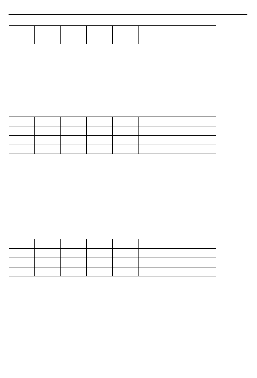
INTEL BUS READ AC TIMING (BTS=0) Figure 3
PW
ALE
t
ASD
ASH
t
CYC
WR
RD
t
ASD
PW
EL
t
CS
CS
t
ASL
AD0–AD7
t
AHL
INTEL BUS WRITE AC TIMING (BTS=0) Figure 4
PW
PW
ASH
t
EL
t
CS
t
ASL
ALE
WR
RD
CS
t
ASD
t
ASD
t
ASED
ASED
PW
EH
t
CH
t
DDR
t
CYC
PW
EH
t
t
DHR
t
DHW
CH
AD0–AD7
031197 16/20
t
t
AHL
DSW
Page 17

MOTOROLA BUS AC TIMING (BTS=1) Figure 5
PW
ASH
AS
DS
R/W
AD0–AD7
(READ)
CS
AD0–AD7
(WRITE)
t
ASD
t
ASL
t
ASL
PW
t
t
AHL
AHL
t
ASED
EL
t
RWS
t
CS
t
DDR
DS2172
PW
EH
t
CYC
t
DSW
t
RWH
t
DHR
t
CH
t
DHW
031197 17/20
Page 18

DS2172
AC CHARACTERISTICS – RECEIVE SIDE (0°C to 70°C; VDD=5V ± 10%)
PARAMETER SYMBOL MIN TYP MAX UNITS NOTES
RCLK Period t
RCLK Pulse Width t
RDATA Set Up to RCLK Rising t
RDATA Hold from RCLK Rising t
RDIS Set Up to RCLK Rising t
RDIS Hold from RCLK Rising t
RL and LC Pulse Width t
CP
CH
t
SU1
HD1
SU2
HD2
WRL
RLCK Rise and Fall Times tR, t
CL
F
19 ns
8
8
ns
ns
4 ns
0 ns
4 ns
0 ns
25 ns
10 ns 1
AC CHARACTERISTICS – TRANSMIT SIDE (0°C to 70°C; VDD=5V ± 10%)
PARAMETER SYMBOL MIN TYP MAX UNITS NOTES
TCLK Period t
TCLK Pulse Width t
TDATA Delay from TCLK Rising t
TDIS Set Up to TCLK Rising t
TDIS Hold from TCLK Rising t
TL Pulse Width t
TL Set Up to TCLK Rising t
TL Hold Off from TCLK Rising t
CP
CH
t
DD
SU
HD
WTL
STL
HTL
TCLK Rise and Fall Time tR, t
CL
F
19 ns
8
8
ns
ns
9 ns
4 ns
0 ns
15 ns
4 ns
0 ns
10 ns 1
NOTE:
1. The maximum rise and fall time is either 10 ns or 10% of tCP whichever is less.
031197 18/20
Page 19
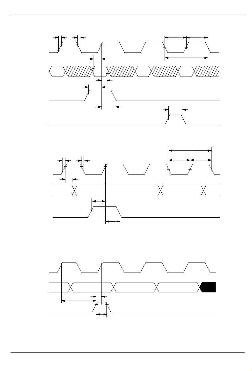
RECEIVE AC TIMING Figure 6
t
R
DS2172
t
t
F
CL
t
CH
RCLK
t
SU1
RDATA
t
SU2
RDIS
RL/LC
TRANSMIT AC TIMING Figure 7
t
R
TCLK
TDATA
TDIS
t
DD
t
CP
t
HD1
t
HD2
t
F
t
WRL
t
CP
t
CL
t
CH
SEE NOTE BELOW
t
SU
t
HD
NOTE: When TDIS is high about the rising edge of TCLK, TDAT A will not be updated and will be held with the previous
valve until TDIS is low about the rising edge of TCLK.
TRANSMIT AC TIMING FOR THE TL INPUT Figure 8
TCLK
TDATA
t
t
HTL
TL
NOTE: The rising edge of TL causes the internal pattern generation circuitry to be reloaded; the first bit of the new
pattern (the shaded one) will appear after two TCLK periods.
STL
t
WTL
031197 19/20
Page 20

DS2172
DS2172 32–PIN TQFP
031197 20/20
GAUGE
 Loading...