

Page 1
DS2165/DS2165Q
DS2165/DS2165Q
16/24/32Kbps ADPCM Processor
FEATURES
• Compresses/expands 64Kbps PCM voice to/from
either 32Kbps, 24Kbps, or 16Kbps
• Dual, fully independent channel architecture; device
can be programmed to perform either:
– two expansions
– two compressions
– one expansion and one compression
• Interconnects directly to combo-codec devices
• Input to output delay is less than 375 µs
• Simple serial port used to configure the device
• Onboard Time Slot Assigner Circuit (TSAC) function
allows data to be input/output at various time slots
• Supports Channel Associated Signaling
• Each channel can be independently idled or placed
into bypass
• Available hardware mode requires no host processor;
ideal for voice storage applications
• Backward-compatible with the DS2167 ADPCM
Processor Chip
• Single +5V supply; low-power CMOS technology
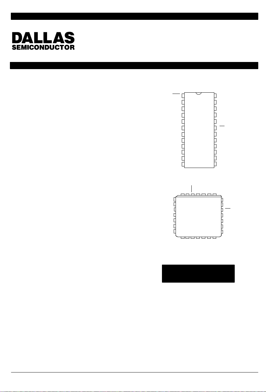
• Available in 24-pin DIP and 28-pin PLCC
PIN ASSIGNMENT
RST
TM0
TM1
A0
A1
A2
A3
A4
A5
SPS
MCLK
VSS
24-Pin DIP (600 MIL)
NC
432
5
6
A0
7
A1
8
A2
9
A3
A4
10
A5
11
12 1314 15 16 1718
A 3–volt Operation Version
is Available (DS2165QL)
1
2
3
4
5
6
7
8
9
10
11
12
TM1
RSTNCVDD
TM0
1
SPS
VSS
MCLK
28-Pin PLCC
NC
272826
XIN
24
23
22
21
20
19
18
17
16
15
14
13
YINCLKX
VDD
YIN
CLKY
FSY
YOUT
CS
SDI
SCLK
XOUT
FSX
CLKX
XIN
CLKY
25
24
23
22
21
20
19
FSX
FSY
YOUT
CS
SDI
SCLK
XOUT
NC
DESCRIPTION
The DS2165 ADPCM Processor Chip is a dedicated
Digital Signal Processing (DSP) chip that has been optimized to perform Adaptive Differential Pulse Code Modulation (ADPCM) speech compression at three different
rates. The chip can be programmed to compress (expand) 64Kbps voice data down to (up from) either
32Kbps, 24Kbps, or 16Kbps. The compression to
32Kbps follows the algorithm specified by CCITT Recommendation G.721 (July 1986) and ANSI document
Copyright 1995 by Dallas Semiconductor Corporation.
All Rights Reserved. For important information regarding
patents and other intellectual property rights, please refer to
Dallas Semiconductor data books.
T1.301 (April 1987). The compression to 24Kbps follows ANSI document T1.303. The compression to
16Kbps follows a proprietary algorithm developed by
Dallas Semiconductor. The DS2165 can switch compression algorithms on-the-fly. This allows the user to
make maximum use of the available bandwidth on a dynamic basis.
041295 1/17
Page 2

DS2165/DS2165Q
OVERVIEW
The DS2165 contains three major functional blocks: a
high performance (10 MIPS) DSP engine, two independent PCM interfaces (X and Y) which connect directly to
serial Time Division Multiplexed (TDM) backplanes, and
a serial port that can configure the device on-the-fly via
an external controller. A 10 MHz master clock is required by the DSP engine. The DS2165 can be configured to perform either two expansions, two compressions, or one expansion and one compression. The
PCM/ADPCM data interfaces support data rates from
256 KHz to 4.096 MHz. Typically, the PCM data rates
will be 1.544 MHz for µ-law and 2.048 MHz for A-law.
Each channel on the device samples the serial input
PCM or ADPCM bit stream during a user-programmed
input time slot, processes the data and outputs the result during a user-programmed output time slot.
Each PCM interface has a control register which specifies functional characteristics (compress, expand, bypass, and idle), data format (µ-law or A-law), and algorithm reset control. With the SPS pin strapped high, the
software mode is enabled and the serial port can be
used to configure the device. In this mode, a novel addressing scheme allows multiple devices to share a
common 3-wire control bus, simplifying system-level interconnect.
With SPS low, the hardware mode is enabled. This
mode disables the serial port and maps certain control
register bits to some of the address and serial port pins.
Under the hardware mode, no external host controller is
required and all PCM/ADPCM input and output time
slots default to time slot 0.
except the IPD bits; the IPD bits for both channels are
set to 1.
SOFTWARE MODE
Tying SPS high enables the software mode. In this
mode, an external host controller writes configuration
data to the DS2165 via the serial port through inputs
SCLK, SDI, and CS
DS2165 is either a 2-byte write or a 4-byte write. A 2byte write consists of the Address/Command Byte
(ACB), followed by a byte to configure the Control Register (CR) for either the X or Y channel. The 4-byte write
consists of the ACB, followed by a byte to configure the
CR, and then one byte to set the input time slot and
another byte to set the output time slot.
. (See Figure 2.) Each write to the
ADDRESS/COMMAND BYTE
In the software mode, the address/command byte is the
first byte written to the serial port; it identifies which of
the 64 possible ADPCM processors sharing the port
wiring is to be updated. Address data must match that at
inputs A0 to A5. If no match occurs, the device ignores
the following configuration data. If an address match occurs, the next three bytes written are accepted as control, input and output time slot data. Bit ACB.6 determines which side (X or Y) of the device is to be updated.
The PCM and ADPCM outputs are tristated during register updates.
CONTROL REGISTER
The control register establishes idle, algorithm reset,
bypass, data format and channel coding for the selected
channel.
HARDWARE RESET
RST allows the user to reset both channel algorithms
and the contents of the internal registers. This pin must
be held low for at least 1 ms on system power-up after
the master clock is stable to ensure that that the device
has initialized properly. RST
when changing to or from the hardware mode. RST
clears all bits of the Control Register for both channels
041295 2/17
should also be asserted
The X and Y side PCM interfaces can be independently
disabled (output 3-stated) via IPD. When IPD is set for
both channels, the device enters a low-power standby
mode. In this mode, the serial port must not be operated
faster than 39 KHz.
ALRST resets the algorithm coefficients for the selected
channel to their initial values. ALRST will be cleared by
the device when the algorithm reset is complete.
Page 3
DS2165/DS2165Q
PIN DESCRIPTION Table 1
PIN SYMBOL TYPE DESCRIPTION
1 RST I Reset. A high-low-high transition resets the algorithm. The device should
2
3
4
5
6
7
8
9
TM0
TM1
A0
A1
A2
A3
A4
A5
10 SPS I Serial Port Select. Tie to VDD to select the serial port; tie to VSS to select
11 MCLK I Master Clock. 10 MHz clock for the ADPCM processing engine; may be
12 V
SS
13 XIN I X Data In. Sampled on falling edge of CLKX during selected time slots.
14 CLKX I X Data Clock. Data clock for the X side PCM interface; must be synchro-
15 FSX I X Frame Sync. 8 KHz frame sync for the X side PCM interface.
16 XOUT O X Data Output. Updated on rising edge of CLKX during selected time slots.
17 SCLK I Serial Data Clock. Used to write to the serial port registers.
18 SDI I Serial Data In. Data for onboard control registers; sampled on the rising
19 CS I Chip Select. Must be low to write to the serial port.
20 YOUT O Y Data Output. Updated on rising edge of CLKY during selected time slots.
21 FSY I Y Frame Sync. 8 KHz frame sync for the Y side PCM interface.
22 CLKY I Y Data Clock. Data clock for the Y side PCM interface; must be synchro-
23 YIN I Y Data In. Sampled on falling edge of CLKY during selected time slots.
24 V
DD
be reset on power up and when changing to or from the hardware mode.
I Test Modes 0 and 1. Tie to VSS for normal operation.
I Address Select. A0 = LSB; A5 = MSB Must match address/command
word to enable the serial port.
the hardware mode.
asynchronous to SCLK, CLKX, and CLKY.
– SIgnal Ground. 0.0 volts.
nous with FSX.
edge of SCLK. LSB sent first.
nous with FSY.
– Positive Supply. 5.0 volts (or 3.0 volts for DS2165QL).
041295 3/17
Page 4
DS2165/DS2165Q
ÉÉ
ÉÉ
DS2165 BLOCK DIAGRAM Figure 1
FSX
CLKX
XIN
XOUT
SCLK
SPS
CS
SDI
A0 - A5
FSY
CLKY
YIN
YOUT
RST
TM0
TM1
X SIDE PCM/ADPCM
DATA INTERFACE
SERIAL PORT CONTROL/
HARDWARE MODE LOGIC
Y SIDE PCM/ADPCM
DATA INTERFACE
RESET AND TEST LOGIC
SERIAL PORT WRITE Figure 2
ADPCM
PROCESSING
ENGINE
MCLK
V
V
DD
SS
A0 A1 A2 A3 A4 A5 X/Y 0 CR0
ADDRESS/COMMAND CONTROL
NOTE:
1. A 2-byte write is shown.
The bypass feature is enabled when BYP is set and IPD
is cleared. During bypass, no expansion or compression occurs. Bypass operates on bytewide (8 bits) slots
when CP/EX
when CP/EX is cleared.
041295 4/17
is set and on nibble-wide (4 bits) slots
CR2 CR3 CR4 CR5 CR6 CR7
CR1
A-law (U/A
= 0) and µ-law (U/A = 1) PCM coding is independently selected for the X and Y channels via CR.2. If
BYP and IPD are cleared, then CP/EX
determines if the
input data is to be compressed or expanded.
Page 5
DS2165/DS2165Q
ADDRESS/COMMAND BYTE Figure 3
(MSB) (LSB)
– X/Y A5 A4 A3 A2 A1 A0
SYMBOL POSITION NAME AND DESCRIPTION
– ACB.7 Reserved; must be 0 for proper operation
X/Y ACB.6 X/Y Channel Select
0 = update channel Y characteristics
1 = update channel X characteristics
A5 ACB.5 MSB of Device Address
A4 ACB.4
A3 ACB.3
A2 ACB.2
A1 ACB.1
A0 ACB.0 LSB of Device Address
CONTROL REGISTER Figure 4
(MSB) (LSB)
AS0 AS1 IPD ALRST BYP U/A AS2 CP/EX
SYMBOL POSITION NAME AND DESCRIPTION
AS0 CR.7 Algorithm Select 0. See Table 2.
AS1 CR.6 Algorithm Select 1. See Table 2.
IPD CR.5 Idle and Power Down.
0 = channel enabled
1 = channel disabled (output 3-stated)
ALRST CR.4 Algorithm Reset.
0 = normal operation
1 = reset algorithm for selected channel
BYP CR.3 Bypass.
0 = normal operation
1 = bypass selected channel
U/A
AS2 CR.1 Algorithm Select 2. See Table 2.
CP/EX
CR.2 Data Format.
0 = A-law
1 = µ-law
CR.0 Channel Coding.
0 = expand (decode) selected channel
1 = compress (encode) selected channel
ALGORITHM SELECT BITS Table 2
ALGORITHM SELECTED AS2 AS1 AS0
64Kbps to/from 32Kbps 0 0 0
64Kbps to/from 24Kbps 1 1 1
64Kbps to/from 16Kbps 1 0 1
041295 5/17
Page 6

DS2165/DS2165Q
INPUT TIME SLOT REGISTER Figure 5
(MSB) (LSB)
– – D5 D4 D3 D2 D1 D0
SYMBOL POSITION NAME AND DESCRIPTION
- ITR.7 Reserved; must be 0 for proper operation.
- ITR.6 Reserved; must be 0 for proper operation.
D5 ITR.5 MSB of input time slot register.
D4 ITR.4
D3 ITR.3
D2 ITR.2
D1 ITR.1
D0 ITR.0 LSB of input time slot register.
OUTPUT TIME SLOT REGISTER Figure 6
(MSB) (LSB)
–
SYMBOL POSITION NAME AND DESCRIPTION
- OTR.7 Reserved; must be 0 for proper operation.
- OTR.6 Reserved; must be 0 for proper operation.
D5 OTR.5 MSB of output time slot register.
D4 OTR.4
D3 OTR.3
D2 OTR.2
D1 OTR.1
D0 OTR.0 LSB of output time slot register.
– D5 D4 D3 D2 D1 D0
TIME SLOT ASSIGNMENT/ORGANIZATION
Onboard counters establish when PCM and ADPCM
I/O occurs. The counters are programmed via the time
slot registers. Time slot size (number of bits wide) is determined by the state of CP/EX
slots available is determined by both the state of CP/EX
and U/A. (See Figures 7 through 10.) For example, if the
X channel is set to compress (CP/EX
041295 6/17
. The number of time
= 1) and it is set to
expect µ-law data (U/A
= 1), then the input port (XIN) is
set up for 32 8-bit time slots and the output port (XOUT)
is set up for 64 4-bit time slots. The time slot organization is not dependent on which algorithm has been selected. NOTE: Time slots are counted from the frame
sync signal starting at the first rising edge of either CLKX
or CLKY after the frame sync.
Page 7

DS2165 µ-LAW PCM INTERFACE Figure 7
TIME SLOT 0 TIME SLOT N TIME SLOT 0TIME SLOT 31
CLKX, CLKY
FSX, FSY
MSB
XIN, YIN
XOUT, YOUT
DON’T CARE
3-STATE
MSB
DS2165 µ-LAW ADPCM INTERFACE Figure 8
CLKX, CLKY
FSX, FSY
TIME
SLOT 0
TIME
SLOT 1
TIME
SLOT N
LSB
LSB
TIME
SLOT 62
DS2165/DS2165Q
DON’T CARE
3-STATE
TIME
SLOT 63
TIME
SLOT 0
...
MSB LSB
XIN, YIN
XOUT, YOUT
DON’T CARE
3-STATE
DS2165 A-LAW PCM INTERFACE Figure 9
TIME SLOT 0 TIME SLOT N TIME SLOT 0TIME SLOT 31
CLKX, CLKY
FSX, FSY
XIN, YIN
XOUT, YOUT
DON’T CARE
3-STATE
MSB
MSB
LSB
LSB
DON’T CARE
3-STATEMSB LSB
...
DON’T CARE
3-STATE
041295 7/17
Page 8

DS2165/DS2165Q
DS2165 A-LAW ADPCM INTERFACE Figure 10
CLKX, CLKY
FSX, FSY
XIN, YIN
TIME
SLOT 0
DON’T CARE
TIME
SLOT 1
MSB LSB
TIME
SLOT N
TIME
SLOT 62
TIME
SLOT 63
DON’T CARE
TIME
SLOT 0
XOUT, YOUT
3-STATE
HARDWARE MODE
The hardware mode is intended for applications that do
not have an external controller available or do not require the extended features offered by the serial port.
Tying the SPS pin to V
disables the serial port, clears
SS
HARDWARE MODE Table 3
PIN # / NAME REG. LOCATION NAME AND DESCRIPTION
4 / A0 CP/EX
5 / A1 AS0/AS1/AS2
6 / A2 U/A
7 / A3 CP/EX
8 / A4 AS0/AS1/AS2
9 / A5 U/A
18 / SDI IPD
19 / CS IPD
(Channel X)
(Channel X & Y)
(Channel X)
(Channel Y)
(Channel X & Y)
(Channel Y)
(Channel Y)
(Channel X)
3-STATEMSB LSB
all internal register bits and maps the IPD, U/A
, and
CP/EX bits for both channels to external bits. (See T able
3.) In the hardware mode, both the input and output time
slots default to time slot 0.
Channel X Coding Configuration
0 = Expand
1 = Compress
Algorithm Select (see Table 5)
Channel X Data Format
0 = A-law
1 = µ-law
Channel Y Coding Configuration
0 = Expand
1 = Compress
Algorithm Select (see Table 5)
Channel Y Data Format
0 = A-law
1 = µ-law
Channel Y Idle Select
0 = Channel active
1 = Channel idle
Channel X Idle Select
0 = Channel active
1 = Channel idle
NOTES:
1. SCLK must be tied to VSS when the hardware mode is selected.
2. When both channels are idled, power consumption is significantly reduced.
3. The DS2165 will power-up within 800 ms after either channel is returned to active from an idle state.
041295 8/17
Page 9

DS2165/DS2165Q
ALGORITHM SELECT FOR HARDWARE MODE Table 4
ALGORITHM CONFIGURATION OF A1 AND A4
64Kbps to/from 32Kbps Tie both A1 and A4 to V
SS.
64Kbps to/from 24Kbps Hold A1 and A4 low during a hardware reset; take both A1 and A4 high after
pin has returned high (allow 3 µs after RST returns high before taking
the RST
A1 and A4 high).
64Kbps to/from 16Kbps Tie both A1 and A4 to V
DD.
DS2165 CONNECTION TO CODEC/FILTER Figure 11
CODEC/FILTER
VFXVFX+
ANALOG
INTERFACE
TRANSMIT DATA CLOCK
RECEIVE DATA CLOCK
RECEIVE FRAME SYNC
TRANSMIT FRAME SYNC
GSX
VFRO
MCLKR
DX
DR
MCLKX
BCLKX
BCLKR
FSR
FSX
NOTE:
Suggested Codec/Filters
TP305X National Semiconductor
ETC505X SGS–Thomson Microelectronics
MC1455XX Motorola
TCM29CXX Texas Instruments
HD44238C Hitachi
*other generic Codec/Filter devices can be substituted.
XIN
YOUT
CLKX
CLKY
FSY
FSX
TM0
TM1
DS2165
RST
RESET
CIRCUITRY
(DS1231)
XOUT
YIN
MCLK
SPS
CS
SCLK
SDI
A0
A1
A2
A3
A4
A5
TRANSMIT DATA
RECEIVE DATA
10 MHz CLOCK
3-WIRE BUS FROM
EXTERNAL CONTROLLER
ADDRESS SELECT
(ADDRESS=0 SHOWN)
041295 9/17
Page 10

DS2165/DS2165Q
PCM AND ADPCM INPUT/OUTPUT
Since the organization of the input and output time slots
on the DS2165 does not depend on the algorithm selected, it always assumes that PCM input and output will
be in 8-bit bytes and that ADPCM input and output will
be in 4-bit bytes. Figure 12 demonstrates how the
DS2165 handles the I/O for the three different algo-
PCM AND ADPCM I/O EXAMPLE Figure 12
CLKX
FSX
MSB LSB
XIN
rithms. In the figure, it is assumed that channel X is in the
compression mode (CP/EX = 1) and channel Y is in the
expansion mode (CP/EX = 0). Also, it is assumed that
both the input and output time slots for both channels
are set to 0.
XOUT (32KBPS)
XOUT (24KBPS)
XOUT (16KBPS)
CLKY
FSY
YIN (32KBPS)
YIN (24KBPS)
YIN (16KBPS)
YOUT
MSB LSB
MSB LSB
SEE NOTE 1
MSB LSB
00
MSB LSB
MSB LSB
MSB LSB
MSB LSB
3-STATE
3-STATE
3–STATE
3-STATE
NOTE:
1. The bit after the LSB in the 24Kbps ADPCM output will only be a 1 when the DS2165 is operated in the software mode and is programmed to perform 24Kbps compression; in all other configurations, it will be a 0.
041295 10/17
Page 11

DS2165/DS2165Q
TIME SLOT RESTRICTIONS
Under certain conditions, the DS2165 does contain
some restrictions on the output time slots that are available. These restrictions are covered in detail in a separate application note. No restrictions occur if the
DS2165 is operated in the hardware mode.
INPUT TO OUTPUT DELAY
With all three compressions algorithms, the total delay,
from the time the PCM data sample is captured by the
DS2165 to the time it is output, is always less than 375
µs. The exact delay is determined by the input and output time slots selected for each channel.
CHANNEL ASSOCIATED SIGNALING
The DS2165 supports Channel Associated Signaling
(CAS) via its ability to automatically change from the
32Kbps compression algorithm to the 24Kbps algorithm. If the DS2165 is configured to perform the 32Kbps
algorithm, then in both the hardware and software
mode, it will sense the frame sync inputs (FSX and FSY)
for a double wide frame sync pulse. Whenever the
DS2165 receives a double wide pulse, it will automatically switch from the 32Kbps algorithm to the 24Kbps algorithm. Switching to the 24Kbps algorithm allows the
user to insert signaling data into the LSB bit position of
the ADPCM output because this bit does not contain
any useful speech information.
ON-THE-FLY ALGORITHM SELECTION
In the software mode, the user can switch between the
three available algorithms on-the-fly. That is, the
DS2165 does not need to be reset or stopped to make
the change from one algorithm to another . The DS2165
reads the Control Register before it starts to process
each PCM or ADPCM sample. If the user wishes to
switch algorithms, then the Control Register must be updated via the serial port before the first input sample to
be processed with the new algorithm arrives at either
XIN or YIN. The PCM and ACPCM outputs will tristate
during register updates.
041295 11/17
Page 12

DS2165/DS2165Q
ABSOLUTE MAXIMUM RATINGS*
Voltage on any Pin Relative to Ground -1.0V to +7.0V
Operating Temperature 0°C to 70°C
Storage Temperature -55°C to +125°C
Soldering Temperature 260°C for 10 seconds
* This is a stress rating only and functional operation of the device at these or any other conditions above
those indicated in the operation sections of this specification is not implied. Exposure to absolute maximum rating conditions for extended periods of time may affect reliability.
RECOMMENDED DC OPERATING CONDITIONS (0°C to 70°C)
PARAMETER SYMBOL MIN TYP MAX UNITS NOTES
Logic 1 V
Logic 0 V
Supply V
Logic 1 V
Logic 0 V
Supply V
IH
IL
DD
IH
IL
DD
2.0 VCC+0.3 V 5
-0.3 +0.8 V 5
4.5 5.5 V 5
2.2 VCC+0.3 V 6
-0.3 +0.4 V 6
2.7 3.6 V 6
CAPACITANCE (tA=25°C)
PARAMETER SYMBOL MIN TYP MAX UNITS NOTES
Input Capacitance C
Output Capacitance C
IN
OUT
5 pF
10 pF
(0°C to 70°C; VDD=5V + 10%)
DC ELECTRICAL CHARACTERISTICS (V
PARAMETER SYMBOL MIN TYP MAX UNITS NOTES
Active Supply Current I
Active Supply Current I
Idle Supply Current I
Input Leakage I
Output Leakage I
Output Current (2.4V) I
Output Current (0.4V) I
Output Current (2.2V) I
Output Current (0.4V) I
DDA
DDA
DDPD
I
O
OH
OL
OH
OL
-1.0 +1.0 µA
-1.0 +1.0 µA 4
-1.0 mA 5
+4.0 mA 5
-0.5 mA 6
+2.0 mA 6
=3.0V + 20% – 10% for DS2165QL)
DD
20 mA 1, 2, 5
12 mA 1, 2, 6
1 mA 1, 2 ,3
NOTES:
1. CLKX = CLKY = 1.544 MHz; MCLK = 10 MHz.
2. Outputs open; inputs swinging full supply levels.
3. Both channels in idle mode.
4. XOUT and YOUT are 3-stated.
5. Applies only to 5V device.
6. Applies only to 3V device (DS2165QL).
041295 12/17
Page 13

DS2165/DS2165Q
PCM INTERFACE (0°C to 70°C; VDD=5V +10%)
AC ELECTRICAL CHARACTERISTICS (V
PARAMETER SYMBOL MIN TYP MAX UNITS NOTES
CLKX, CLKY Period t
CLKX, CLKY Pulse Width t
CLKX, CLKY Rise Fall Times t
Hold Time from CLKX, CLKY
to FSX, FSY
Setup Time from FSX, FSY
high to CLKX, CLKY low
Hold Time from CLKX, CLKY
low to FSX, FSY low
Setup Time for XIN, YIN to
CLKX, CLKY low
Hold Time for XIN, YIN
to CLKX, CLKY low
Delay Time from CLKX,
CLKY to Valid XOUT, YOUT
Delay Time from CLKX,
CLKY to XOUT, YOUT 3-stated
PXY
WXYL
t
WXYH
RXY
t
FXY
t
HOLD
t
SF
t
HF
t
SD
t
HD
t
DXYO
t
DXYZ
244 3906 ns 1
100 ns
0 ns 2
50 ns 2
100 ns 2
50 ns 2
50 ns 2
10 150 ns 3
20 150 ns 2,3,4
=3.0V + 20% – 10% for DS2165QL)
DD
10 20 ns
NOTES:
1. Maximum width of FSX and FSY is one CLKX or CLKY period (except for signaling frames).
2. Measured at V
= 2.0V, VIL = 0.8V , and 10 ns maximum rise and fall times.
IH
3. Load = 150 pF + 2 LSTTL loads.
4. For LSB of PCM or ADPCM byte.
MASTER CLOCK/RESET (0°C to 70°C; VDD=5V + 10%)
AC ELECTRICAL CHARACTERISTICS (V
PARAMETER SYMBOL MIN TYP MAX UNITS NOTES
MCLK Period t
MCLK Pulse Width t
MCLK Rise/Fall Times tRM, t
RST Pulse Width t
PM
WMH
t
WML
RST
FM
,
45 50 55 ns
1 ms
=3.0V + 20% – 10% for DS2165QL)
DD
100 ns 1
10 ns
NOTE:
1. MCLK = 10 MHz + 500 ppm
041295 13/17
Page 14

DS2165/DS2165Q
SERIAL PORT (0°C to 70°C; VDD=5V + 10%)
AC ELECTRICAL CHARACTERISTICS (V
PARAMETER SYMBOL MIN TYP MAX UNITS NOTES
SDI to SCLK Set Up t
SCLK to SDI Hold t
DC
CDH
SCLK Low Time t
SCLK High Time t
CH
SCLK Rise and Fall Time tR, t
CS to SCLK Setup t
SCLK to CS Hold t
CS Inactive Time t
SCLK Setup to CS Falling t
CC
CCH
CWH
SCC
CL
F
55 ns 1
55 ns 1
250 ns 1
250 ns 1
50 ns 1
250 ns 1
250 ns 1
50 ns 1
=3.0V + 20% – 10% for DS2165QL)
DD
100 ns 1
NOTE:
1. Measured at V
= 2.0V , V
IH
= 0.8V , and 10ns maximum rise and fall times.
IL
PCM INTERFACE AC TIMING DIAGRAM Figure 13
t
PXY
CLKX
CLKY
t
HOLD
t
RXY
t
FXY
t
WXYH
t
WXYL
FSX
FSY
FSX
FSY
XIN
YIN
XOUT
YOUT
041295 14/17
3-STATE
t
HF
t
SF
t
HF
(MSB)
t
DXYO
(MSB)
t
SD
t
HD
t
DXYZ
Page 15

MASTER CLOCK/RESET AC TIMING DIAGRAM Figure 14
t
FM
MCLK
RST
t
RST
t
RM
SERIAL PORT AC TIMING DIAGRAM Figure 15
CS
t
CWH
t
SCC
t
t
CC
t
CH
R
t
F
t
WMH
t
CCH
DS2165/DS2165Q
t
PM
t
WML
t
CWH
SCLK
t
CL
t
DC
SDI
t
CDH
NOTE:
1. SCLK may be either high or low when CS is taken low.
041295 15/17
Page 16

DS2165/DS2165Q
DS2165 16/24/32KBPS ADPCM PROCESSOR 24–PIN DIP
B
1
A
K
PKG 24-PIN
DIM MIN MAX
A IN.MM1.150
B IN.MM0.250
C IN.MM0.120
D IN.MM0.300
E IN.MM0.015
F IN.MM0.125
G IN.MM0.090
H INMM0.320
J INMM0.008
K IN.MM0.015
29.21
6.35
3.05
7.62
0.38
3.18
2.23
8.13
0.20
0.38
1.260
32.00
0.270
6.86
0.140
3.56
0.325
8.26
0.040
1.02
0.135
3.48
0.110
2.79
0.370
9.40
0.012
0.30
0.022
0.56
D
E
C
J
F
G
H
041295 16/17
Page 17

DS2165Q 16/24/32KBPS ADPCM PROCESSOR 28-PIN PLCC
E
E1
N
1
CH1
D1 D D2
e1
DS2165/DS2165Q
B
L1
B1
E2
INCHES
DIM MIN MAX
A 0.165 0.180
A1 0.090 0.120
A2 0.020 –
B 0.026 0.033
B1 0.013 0.021
C 0.009 0.012
D 0.485 0.495
D1 0.450 0.456
D2 0.390 0.430
E 0.485 0.495
E1 0.450 0.456
E2 0.390 0.430
L1 0.060 –
N 28 –
e1 0.050 BSC
CH1 0.042 0.048
C
A1A2
A
This drawing controlled by drawing number 56–G4001–001.
041295 17/17
 Loading...