

Page 1
DS2152
PRELIMINARY
DS2152
Enhanced T1 Single Chip Transceiver
FEATURES
• Complete DS1/ISDN–PRI transceiver functionality
• Line interface can handle both long and short haul
trunks
• 32–bit or 128–bit crystal–less jitter attenuator
• Generates DSX–1 and CSU line build outs
• Frames to D4, ESF, and SLC–96
R
formats
• Dual onboard two–frame elastic store slip buffers that
can connect to asynchronous backplanes up to
8.192 MHz
• 8–bit parallel control port that can be used directly on
either multiplexed or non–multiplexed buses (Intel or
Motorola)
• Extracts and inserts robbed bit signaling
• Detects and generates yellow (RAI) and blue (AIS)
alarms
• Programmable output clocks for Fractional T1
• Fully independent transmit and receive functionality
• Integral HDLC controller with 16–byte buffers for the
FDL
• Generates and detects in–band loop codes from 1 to
8 bits in length including CSU loop codes
• Contains ANSI one’s density monitor and enforcer
• Large path and line error counters including BPV , CV ,
CRC6, and framing bit errors
• Pin compatible with DS2154 E1 Enhanced Single–
Chip Transceiver
• 5V supply; low power CMOS
• 100–pin 14mm
2
body LQFP package
PIN ASSIGNMENT
100
1
ORDERING INFORMATION
DS2152L (0°C to 70°C)
DS2152LN (–40°C to +85°C)
DESCRIPTION
The DS2152 T1 Enhanced Single–Chip Transceiver
contains all of the necessary functions for connection to
T1 lines whether they be DS–1 long haul or DSX–1 short
haul. The clock recovery circuitry automatically adjusts
to T1 lines from 0 feet to over 6000 feet in length. The
device can generate both DSX–1 line build outs as well
as CSU line build outs of –7.5 dB, –15 dB, and –22.5 dB.
Copyright 1997 by Dallas Semiconductor Corporation.
All Rights Reserved. For important information regarding
patents and other intellectual property rights, please refer to
Dallas Semiconductor data books.
The onboard jitter attenuator (selectable to either 32 bits
or 128 bits) can be placed in either the transmit or
receive data paths. The framer locates the frame and
multiframe boundaries and monitors the data stream for
alarms. It is also used for extracting and inserting
robbed–bit signaling data and FDL data. The device
contains a set of internal registers which the user can
031897 1/79
Page 2

DS2152
access and control the operation of the unit. Quick
access via the parallel control port allows a single controller to handle many T1 lines. The device fully meets
all of the latest T1 specifications including ANSI
T1.403–1995, ANSI T1.231–1993, AT&T TR 62411
(12–90), AT&T TR54016, and ITU G.703, G.704,
G.706, G.823, and I.431.
1.0 INTRODUCTION
The DS2152 is a superset version of the popular
DS2151 T1 Single–Chip Transceiver offering the new
features listed below. All of the original features of the
DS2151 have been retained and software created for
the original devices is transferable into the DS2152.
New Features
• option for non–multiplexed bus operation
• crystal–less jitter attenuation
• addtional hardware signaling capability including:
– receive signaling reinsertion to a backplane mul-
tiframe sync
– availability of signaling in a separate PCM data
stream
– signaling freezing
– interrupt generated on change of signaling data
• per–channel code insertion in both transmit and
receive paths
• full HDLC controller for the FDL with 16–byte buffers
in both transmit and receive paths
• RCL, RLOS, RRA, and RAIS alarms now interrupt on
change of state
• 8.192 MHz clock synthesizer
• per–channel loopback
• addition of hardware pins to indicate carrier loss &
signaling freeze
• line interface function can be completely decoupled
from the framer/formatter to allow:
– interface to optical, HDSL, and other NRZ inter-
faces
– be able to “tap” the transmit and receive bipolar
data streams for monitoring purposes
– be able corrupt data and insert framing errors,
CRC errors, etc.
• transmit and receive elastic stores now have indepen-
dent backplane clocks
• ability to monitor one DS0 channel in both the transmit
and receive paths
• access to the data streams in between the framer/for-
matter and the elastic stores
• AIS generation in the line interface that is independent
of loopbacks
• ability to calculate and check CRC6 according to the
Japanese standard
• ability to pass the F–Bit position through the elastic
stores in the 2.048 MHz backplane mode
• programmable in–band loop code generator and
detector
Functional Description
The analog AMI/B8ZS waveform off of the T1 line is
transformer coupled into the RRING and RTIP pins of
the DS2152. The device recovers clock and data from
the analog signal and passes it through the jitter attenuation mux to the receive side framer where the digital
serial stream is analyzed to locate the framing/multiframe pattern. The DS2152 contains an active filter that
reconstructs the analog received signal for the non–linear losses that occur in transmission. The device has a
usable receive sensitivity of 0 dB to –36 dB which allows
the device to operate on cables up to 6000 feet in length.
The receive side framer locates D4 (SLC–96) or ESF
multiframe boundaries as well as detects incoming
alarms including, carrier loss, loss of synchronization,
blue (AIS) and yellow alarms. If needed, the receive
side elastic store can be enabled in order to absorb the
phase and frequency differences between the recovered T1 data stream and an asynchronous backplane
clock which is provided at the RSYSCLK input. The
clock applied at the RSYSCLK input can be either a
2.048 MHz clock or a 1.544 MHz clock. The RSYSCLK
can be a bursty clock with speeds up to 8.192 MHz.
The transmit side of the DS2152 is totally independent
from the receive side in both the clock requirements and
characteristics. Data off of a backplane can be passed
through a transmit side elastic store if necessary. The
transmit formatter will provide the necessary frame/multiframe data overhead for T1 transmission. Once the
data stream has been prepared for transmission, it is
sent via the jitter attenuation mux to the waveshaping
and line driver functions. The DS2152 will drive the T1
line from the TTIP and TRING pins via a coupling transformer. The line driver can handle both long (CSU) and
short haul (DSX–1) lines.
031897 2/79
Page 3

DS2152
Reader’s Note
This data sheet assumes a particular nomenclature of
the T1 operating environment. In each 125 us frame,
there are 24 eight–bit channels plus a framing bit. It is
assumed that the framing bit is sent first followed by
D4 Superframe (12 frames per multiframe) Multiframe Structure
SLC–96 Subscriber Loop Carrier – 96 Channels (SLC–96 is an AT&T registered trademark)
ESF Extended Superframe (24 frames per multiframe) Multiframe Structure
B8ZS Biploar with 8 Zero Subsitution
CRC Cyclical Redundancy Check
Ft Terminal Framing Pattern in D4
Fs Signaling Framing Pattern in D4
FPS Framing Pattern in ESF
MF Multiframe
BOC Bit Oriented Code
HDLC High Level Data Link Control
FDL Facility Data LInk
channel 1. Each channel is made up of eight bits which
are numbered 1 to 8. Bit number 1 is the MSB and is
transmitted first. Bit number 8 is the LSB and is transmitted last. Throughout this data sheet, the following
abbreviations will be used:
031897 3/79
Page 4
DS2152
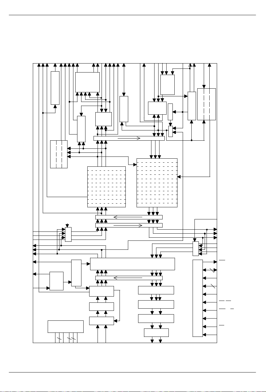
DS2152 ENHANCED T1 SINGLE–CHIP TRANSCEIVER Figure 1–1
RCL
RCLK
RLOS/LOTC
8MCLK
RLINK
RLCLK
RCHBLK
RCHCLK
RSIGF
RSIG
RSER
RSYNC
RMSYNC
RFSYNC
RDATA
RPOSI
RCLKI
RNEGI
RNEGO
RCLKO
RPOSO
8XCLK
XTALD
MCLK
Synthesizer
8.192 MHz Clock
FDL Extraction
16 Byte Buffer
BOM Detection
12.352 MHz
Clock/
Cystral
Interface
Power Connections
4
LIUC
mux
1.544
MHz
3
Signaling
Timing Control
Receive Side Framer
VCO/PLL
24.7MHz
4
RSYSCLK
TSYNC
Buffer
Sync Control
Store
Elastic
Payload Loopback
sync
clock
data
Per–Channel Code Insert
Channel Marking
Signaling Extraction
One’s Density Monitor
CRC/Frame Error Count
Loop Code Detector
Alarm Detection
Synchronizer
BPV Counter
B8ZS Decoder
Framer Loopback
Remote Loopback
(Can be placed in either tramsmit or receive path)
Jitter Attenuation
Local Loopback
Clock/Data
Recovery
Peak Detect
Filter
TSEO
TDATA
sync
Per–Channel Code Insert
Per–Channel Loopback
Signaling Insertion
Clear Channel
FDL Insertion
Loop Code Generation
F–Bit Insertion
CRC Generation
Yellow Alarm Generation
One’s Density Enforcer
B8ZS Encode
AIS Generation
Transmit Side Formatter
LIU AIS Generation
Wave Shaping
CSU Filters
Line Drivers
TSSYNC
TSYSCLK
TSER
Store
Elastic
clock
data
TSIG
Insertion
Signaling
Hardware
LOTC
mux
TCLK
TCHBLK
Timing Control
TCHCLK
TLINK
TLCLK
FDL Insertion
16–Byte Buffer
BOM Generation
LIUC
TPOSO
TCLKO
TNEGO
TNEGI
mux
TCLKI
TPOSI
INT
D0 to D7/AD0 to AD7
8
MUX
A0 to A6
7
ALE(AS)/A7
RD
WR
(routed to all blocks)
Paralle and Test Control Port
BTS
CS
TEST
(DS)
(R/W)
031897 4/79
RVDD
TVDD
DVDD
RVSS
TVSS
DVSS
RRING
RTIP
TRING
TTIP
Page 5

PIN LIST Table 1–1
PIN SYMBOL TYPE DESCRIPTION
1 RCHBLK O Receive Channel Block
2 NC – No Connect
3 8MCLK O 8.192 MHz Clock
4 NC – No Connect
5 NC – No Connect
6 RCL O Receive Carrier Loss
7 NC – No Connect
8 NC – No Connect
9 NC – No Connect
10 NC – No Connect
11 BTS I Bus Type Select
12 LIUC I Line Interface Connect
13 8XCLK O Eight Times Clock
14 TEST I Test
15 NC – No Connect
16 RTIP I Receive Analog Tip Input
17 RRING I Receive Analog Ring Input
18 RVDD – Receive Analog Positive Supply
19 RVSS – Receive Analog Signal Ground
20 RVSS – Receive Analog Signal Ground
21 MCLK I Master Clock Input
22 XTALD O Quartz Crystal Driver
23 NC – No Connect
24 RVSS – Receive Analog Signal Ground
25 INT O Interrupt
26 NC – No Connect
27 NC – No Connect
28 NC – No Connect
29 TTIP O Transmit Analog Tip Output
30 TVSS – Transmit Analog Signal Ground
31 TVDD – Transmit Analog Positive Supply
32 TRING O Transmit Analog Ring Output
33 TCHBLK O Transmit Channel Block
34 TLCLK O Transmit Link Clock
DS2152
031897 5/79
Page 6

DS2152
PIN DESCRIPTIONTYPESYMBOL
35 TLINK I Transmit Link Data
36 NC – No Connect
37 TSYNC I/O Transmit Sync
38 TPOSI I Transmit Positive Data Input
39 TNEGI I Transmit Negative Data Input
40 TCLKI I Transmit Clock Input
41 TCLKO O T ransmit Clock Output
42 TNEGO O Transmit Negative Data Output
43 TPOSO O T ransmit Positive Data Output
44 DVDD – Digital Positive Supply
45 DVSS – Digital Signal Ground
46 TCLK I Transmit Clock
47 TSER I Transmit Serial Data
48 TSIG I Transmit Signaling Input
49 TESO O Transmit Elastic Store Output
50 TDATA I Transmit Data
51 TSYSCLK I Transmit System Clock
52 TSSYNC I Transmit System Sync
53 TCHCLK O Transmit Channel Clock
54 NC – No Connect
55 MUX I Bus Operation
56 D0/AD0 I/O Data Bus Bit 0 / Address/Data Bus Bit 0
57 D1/AD1 I/O Data Bus Bit 1 / Address/Data Bus Bit 1
58 D2/AD2 I/O Data Bus Bit 2 / Address/Data Bus Bit 2
59 D3/AD3 I/O Data Bus Bit 3 / Address/Data Bus Bit 3
60 DVSS – Digital Signal Ground
61 DVDD – Digital Positive Supply .
62 D4/AD4 I/O Data Bus Bit 4 / Address/Data Bus Bit 4
63 D5/AD5 I/O Data Bus Bit 5 / Address/Data Bus Bit 5
64 D6/AD6 I/O Data Bus Bit 6 / Address/Data Bus Bit 6
65 D7/AD7 I/O Data Bus Bit 7 / Address/Data Bus Bit 7
66 A0 I Address Bus Bit 0
67 A1 I Address Bus Bit 1
68 A2 I Address Bus Bit 2
69 A3 I Address Bus Bit 3
031897 6/79
Page 7

PIN DESCRIPTIONTYPESYMBOL
70 A4 I Address Bus Bit 4
71 A5 I Address Bus Bit 5
72 A6 I Address Bus Bit 6
73 A7/ALE I Address Bus Bit 7 / Address Latch Enable
74 RD (DS) I Read Input (Data Strobe)
75 CS I Chip Select
76 NC – No Connect
77 WR (R/W) I Write Input (Read/Write)
78 RLINK O Receive Link Data
79 RLCLK O Receive Link Clock
80 DVSS – Digital SIgnal Ground
81 DVDD – Digital Positive Supply
82 RCLK O Receive Clock
83 DVDD – Digital Positive Supply
84 DVSS – Digital Signal Ground
85 RDATA O Receive Data
86 RPOSI I Receive Positive Data Input
87 RNEGI I Receive Negative Data Input
88 RCLKI I Receive Clock Input
89 RCLKO O Receive Clock Output
90 RNEGO O Receive Negative Data Output
91 RPOSO O Receive Positive Data Output
92 RCHCLK O Receive Channel Clock
93 RSIGF O Receive Signaling Freeze Output
94 RSIG O Receive Signaling Output
95 RSER O Receive Serial Data
96 RMSYNC O Receive Multiframe Sync
97 RFSYNC O Receive Frame Sync
98 RSYNC I/O Receive Sync
99 RLOS/LOTC O Receive Loss Of Sync / Loss Of Transmit Clock
100 RSYSCLK I Receive System Clock
DS2152
NOTE:
Leave all no connect (NC) pins open circuited.
031897 7/79
Page 8

DS2152
DS2152 PIN DESCRIPTION Table 1–2
TRANSMIT SIDE DIGITAL PINS
Transmit Clock [TCLK]. A 1.544 MHz primary clock.
Used to clock data through the transmit side formatter.
this pin is set to output pulses at frame boundaries, it can
also be set via TCR2.4 to output double–wide pulses at
signaling frames. See Section 15 for details.
Transmit Serial Data [TSER]. Transmit NRZ serial
data. Sampled on the falling edge of TCLK when the
transmit side elastic store is disabled. Sampled on the
falling edge of TSYSCLK when the transmit side elastic
store is enabled.
Transmit Channel Clock [TCHCLK]. A 192 KHz clock
which pulses high during the LSB of each channel. Synchronous with TCLK when the transmit side elastic
store is disabled. Synchronous with TSYSCLK when
the transmit side elastic store is enabled. Useful for parallel to serial conversion of channel data.
Transmit Channel Block [TCHBLK]. A user programmable output that can be forced high or low during any of
the 24 T1 channels. Synchronous with TCLK when the
transmit side elastic store is disabled. Synchronous
with TSYSCLK when the transmit side elastic store is
enabled. Useful for blocking clocks to a serial UART or
LAPD controller in applications where not all T1 channels are used such as Fractional T1, 384 Kbps (H0),
768 Kbps or ISDN–PRI . Also useful for locating individual channels in drop–and–insert applications, for external per–channel loopback, and for per–channel conditioning. See Section 9 for details.
Transmit System Clock [TSYSCLK]. 1.544 MHz or
2.048 MHz clock. Only used when the transmit side
elastic store function is enabled. Should be tied low in
applications that do not use the transmit side elastic
store. Can be burst at rates up to 8.192 MHz.
Transmit Link Clock [TLCLK]. 4 KHz or 2 KHz
(ZBTSI) demand clock for the TLINK input. See Section
11 for details.Transmit Link Data [TLINK].
Transmit Link Data [TLINK]. If enabled via TCR1.2,
this pin will be sampled on the falling edge of TCLK for
data insertion into either the FDL stream (ESF) or the
Fs–bit position (D4) or the Z–bit position (ZBTSI). See
Section 11 for details.
Transmit Sync [TSYNC]. A pulse at this pin will establish either frame or multiframe boundaries for the transmit side. Via TCR2.2, the DS2152 can be programmed
to output either a frame or multiframe pulse at this pin. If
Transmit System Sync [TSSYNC]. Only used when
the transmit side elastic store is enabled. A pulse at this
pin will establish either frame or multiframe boundaries
for the transmit side. Should be tied low in applications
that do not use the transmit side elastic store.
Transmit Signaling Input [TSIG]. When enabled, this
input will sample signaling bits for reinsertion into outgoing PCM T1 data stream. Sampled on the falling edge
of TCLK when the transmit side elastic store is disabled.
Sampled on the falling edge of TSYSCLK when the
transmit side elastic store is enabled.
Transmit Elastic Store Data Output [TESO].
Updated on the rising edge of TCLK with data out of the
the transmit side elastic store whether the elastic store
is enabled or not. This pin is normally tied to TDATA.
Transmit Data [TDATA]. Sampled on the falling edge
of TCLK with data to be clocked through the transmit
side formatter. This pin is normally tied to TESO.
Transmit Positive Data Output [TPOSO]. Updated on
the rising edge of TCLKO with the bipolar data out of the
transmit side formatter. Can be programmed to source
NRZ data via the Output Data Format (CCR1.6) control
bit. This pin is normally tied to TPOSI.
Transmit Negative Data Output [TNEGO]. Updated
on the rising edge of TCLKO with the bipolar data out of
the transmit side formatter . This pin is normally tied to
TNEGI.
Transmit Clock Output [TCLKO]. Buf fered clock that
is used to clock data through the transmit side formatter
(i.e., either TCLK or RCLKI). This pin is normally tied to
TCLKI.
Transmit Positive Data Input [TPOSI]. Sampled on
the falling edge of TCLKI for data to be transmitted out
onto the T1 line. Can be internally connected to TPOSO
by tying the LIUC pin high. TPOSI and TNEGI can be
tied together in NRZ applications.
Transmit Negative Data Input [TNEGI]. Sampled on
the falling edge of TCLKI for data to be transmitted out
031897 8/79
Page 9

DS2152
onto the T1 line. Can be internally connected to TNEGO
by tying the LIUC pin high. TPOSI and TNEGI can be
tied together in NRZ applications.
Transmit Clock Input [TCLKI]. Line interface transmit
clock. Can be internally connected to TCLKO by tying
the LIUC pin high.
RECEIVE SIDE DIGITAL PINS
Receive Link Data [RLINK]. Updated with either FDL
data (ESF) or Fs bits (D4) or Z bits (ZBTSI) one RCLK
before the start of a frame. See Section 15 for details.
Receive Link Clock [RLCLK]. A 4 KHz or 2 KHz
(ZBTSI) clock for the RLINK output.
Receive Clock [RCLK]. 1.544 MHz clock that is used
to clock data through the receive side framer.
Receive Channel Clock [RCHCLK]. A 192 KHz clock
which pulses high during the LSB of each channel.
Synchronous with RCLK when the receive side elastic
store is disabled. Synchronous with RSYSCLK when
the receive side elastic store is enabled. Useful for parallel to serial conversion of channel data.
Receive Channel Block [RCHBLK]. A user programmable output that can be forced high or low during any of
the 24 T1 channels. Synchronous with RCLK when the
receive side elastic store is disabled. Synchronous with
RSYSCLK when the receive side elastic store is
enabled. Useful for blocking clocks to a serial UART or
LAPD controller in applications where not all T1 channels are used such as Fractional T1, 384K bps service,
768K bps, or ISDN–PRI. Also useful for locating individual channels in drop–and–insert applications, for external per–channel loopback, and for per–channel conditioning. See Section 9 for details.
Receive Serial Data [RSER]. Received NRZ serial
data. Updated on rising edges of RCLK when the
receive side elastic store is disabled. Updated on the
rising edges of RSYSCLK when the receive side elastic
store is enabled.
Receive Sync [RSYNC]. An extracted pulse, one
RCLK wide, is output at this pin which identifies either
frame (RCR2.4=0) or multiframe (RCR2.4=1) boundaries. If set to output frame boundaries then via
RCR2.5, RSYNC can also be set to output double–wide
pulses on signaling frames. If the receive side elastic
store is enabled via CCR1.2, then this pin can be
enabled to be an input via RCR2.3 at which a frame or
multiframe boundary pulse is applied. See Section 15
for details.
Receive Frame Sync [RFSYNC]. An extracted 8 KHz
pulse, one RCLK wide, is output at this pin which identifies frame boundaries.
Receive Multiframe Sync [RMSYNC]. Only used
when the receive side elastic store is enabled. An
extracted pulse, one RSYSCLK wide, is output at this
pin which identifies multiframe boundaries. If the
receive side elastic store is disabled, then this output will
output multiframe boundaries associated with RCLK.
Receive Data [RDA T A]. Updated on the rising edge of
RCLK with the data out of the receive side framer.
Receive System Clock [RSYSCLK]. 1.544 MHz or
2.048 MHz clock. Only used when the elastic store
function is enabled. Should be tied low in applications
that do not use the elastic store. Can be burst at rates up
to 8.192 MHz.
Receive Signaling Output [RSIG]. Outputs signaling
bits in a PCM format. Updated on rising edges of RCLK
when the receive side elastic store is disabled. Updated
on the rising edges of RSYSCLK when the receive side
elastic store is enabled.
Receive Loss of Sync / Loss of Transmit Clock
[RLOS/LOTC]. A dual function output that is controlled
by the CCR3.5 control bit. This pin can be programmed
to either toggle high when the synchronizer is searching
for the frame and multiframe or to toggle high if the TCLK
pin has not been toggled for 5 usec.
Receive Carrier Loss [RCL]. Set high when the line
interface detects a loss of carrier.
Receive Signaling Freeze [RSIGF]. Set high when the
signaling data is frozen via either automatic or manual
intervention. Used to alert downstream equipment of
the condition.
8 MHz Clock [8MCLK]. A 8.192 MHz output clock that
is referenced to the clock that is output at the RCLK pin
031897 9/79
Page 10

DS2152
and is used to clock data through the receive side
framer.
Receive Positive Data Output [RPOSO]. Updated on
the rising edge of RCLKO with the bipolar data out of the
line interface. This pin is normally tied to RPOSI.
Receive Negative Data Output [RNEGO]. Updated
on the rising edge of RCLKO with the bipolar data out of
the line interface. This pin is normally tied to RNEGI.
Receive Clock Output [RCLKO]. Buffered recovered
clock from the T1 line. This pin is normally tied to RCLKI.
Receive Positive Data Input [RPOSI]. Sampled on
the falling edge of RCLKI for data to be clocked through
the receive side framer. RPOSI and RNEGI can be tied
together for a NRZ interface. Can be internally connected to RPOSO by tying the LIUC pin high.
Receive Negative Data Input [RNEGI]. Sampled on
the falling edge of RCLKI for data to be clocked through
the receive side framer. RPOSI and RNEGI can be tied
together for a NRZ interface. Can be internally connected to RNEGO by tying the LIUC pin high.
Receive Clock Input [RCLKI]. Clock used to clock
data through the receive side framer. This pin is normally tied to RCLKO. Can be internally connected to
RCLKO by tying the LIUC pin high.
PARALLEL CONTROL PORT PINS
Interrupt [INT]. Flags host controller during conditions
and change of conditions defined in the Status Registers 1 and 2 and the FDL Status Register. Active low,
open drain output.
3–State Control [Test]. Set high to 3–state all output
and I/O pins (including the parallel control port). Set low
for normal operation. Useful in board level testing.
Bus Operation [MUX]. Set low to select non–multiplexed bus operation. Set high to select multiplexed bus
operation.
Data Bus [D0 to D7] or Address/Data Bus [AD0 to
AD7]. In non–multiplexed bus operation (MUX = 0),
serves as the data bus. In multiplexed bus operation
(MUX = 1), serves as a 8–bit multiplexed address / data
bus.
Address Bus [A0 to A6]. In non–multiplexed bus
operation (MUX = 0), serves as the address bus. In multiplexed bus operation (MUX = 1), these pins are not
used and should be tied low.
Bus Type Select [BTS]. Strap high to select Motorola
bus timing; strap low to select Intel bus timing. This pin
controls the function of the RD
(DS), ALE(AS), and
WR(R/W) pins. If BTS = 1, then these pins assume the
function listed in parenthesis ().
Read Input [RD
] (Data Strobe [DS]). RD and DS are
active low signals.
Chip Select [CS
]. Must be low to read or write to the
device. CS is an active low signal.
A7 or Address Latch Enable [ALE] (Address Strobe
[AS]). In non–multiplexed bus operation (MUX = 0),
serves as the upper address bit. In multiplexed bus
operation (MUX = 1), serves to demultiplex the bus on a
positive–going edge.
Write Input [WR
] (Read/Write [R/W]). WR is an active
low signal.
LINE INTERFACE PINS
Master Clock Input [MCLK]. A 1.544 MHz (± 50 ppm)
clock source with TTL levels is applied at this pin. This
clock is used internally for both clock/data recovery and
for jitter attenuation. A quartz crystal of 1.544 MHz may
be applied across MCLK and XTALD instead of the TTL
level clock source.
Quartz Crystal Driver [XTALD]. A quartz crystal of
1.544 MHz may be applied across MCLK and XTALD
instead of a TTL level clock source at MCLK. Leave
open circuited if a TTL clock source is applied at MCLK.
Eight Times Clock [8XCLK]. A 12.352 MHz clock that
is frequency locked to the 1.544 MHz clock provided
from the clock/data recovery block (if the jitter attenuator
is enabled on the receive side) or from the TCLKI pin (if
the jitter attenuator is enabled on the transmit side). Can
be internally disabled via the TEST2 register if not
needed.
Line Interface Connect [LIUC]. Tie low to separate the
line interface circuitry from the framer/formatter circuitry
and activate the TPOSI/TNEGI/TCLKI/RPOSI/RNEGI/
031897 10/79
Page 11

DS2152
RCLKI pins. Tie high to connect the the line interface circuitry to the framer/formatter circuitry and deactivate
Receive Analog Positive Supply [RVDD]. 5.0 volts ±
5%. Should be tied to the DVDD and TVDD pins.
the TPOSI/TNEGI/TCLKI/RPOSI/RNEGI/RCLKI pins.
When LIUC is tied high, the TPOSI/TNEGI/TCLKI/
RPOSI/RNEGI/RCLKI pins should be tied low.
Receive Tip and Ring [RTIP & RRING]. Analog inputs
for clock recovery circuitry. These pins connect via a 1:1
Transmit Analog Positive Supply [TVDD]. 5.0 volts ±
5%. Should be tied to the RVDD and DVDD pins.
Digital Signal Ground [DVSS]. Should be tied to the
RVSS and TVSS pins.
transformer to the T1 line. See Section 14 for details.
Receive Analog Signal Ground [RVSS]. 0.0 volts.
Transmit Tip and Ring [TTIP & TRING]. Analog line
Should be tied to the DVSS and TVSS pins.
driver outputs. These pins connect via a 1:1.15 or
1:1.36 step–up transformer to the T1 line. See Section
14 for details.
Transmit Analog Ground [TVSS]. 0.0 volts. Should
be tied to the RVSS and DVSS pins.
SUPPLY PINS
Digital Positive Supply [DVDD]. 5.0 volts ± 5%.
Should be tied to the RVDD and TVDD pins.
DS2152 REGISTER MAP Table 1–3
ADDRESS R/W REGISTER NAME REGISTER ABBREVIATION
00 R/W FDL Control FDLC
01 R/W FDL Status FDLS
02 R/W FDL Interrupt Mask FIMR
03 R/W Receive Performance Report Message RPRM
04 R/W Receive Bit Oriented Code RBOC
05 R Receive FDL FIFO RFFR
06 R/W Transmit Performance Report Message TPRM
07 R/W Transmit Bit Oriented Code TBOC
08 W Transmit FDL FIFO TFFR
09 R/W Test 2 TEST2 (set to 00h)
0A R/W Common Control 7 CCR7
0B – not present –
0C – not present –
0D – not present –
0E – not present –
0F R Device ID IDR
10 R/W Receive Information 3 RIR3
11 R/W Common Control 4 CCR4
12 R/W In–Band Code Control IBCC
031897 11/79
Page 12

DS2152
ADDRESS REGISTER ABBREVIATIONREGISTER NAMER/W
13 R/W Transmit Code Definition TCD
14 R/W Receive Up Code Definition RUPCD
15 R/W Receive Down Code Definition RDNCD
16 R/W Transmit Channel Control 1 TCC1
17 R/W Transmit Channel Control 2 TCC2
18 R/W Transmit Channel Control 3 TCC3
19 R/W Common Control 5 CCR5
1A R Transmit DS0 Monitor TDS0M
1B R/W Receive Channel Control 1 RCC1
1C R/W Receive Channel Control 2 RCC2
1D R/W Receive Channel Control 3 RCC3
1E R/W Common Control 6 CCR6
1F R Receive DS0 Monitor RDS0M
20 R/W Status 1 SR1
21 R/W Status 2 SR2
22 R/W Receive Information 1 RIR1
23 R Line Code Violation Count 1 LCVCR1
24 R Line Code Violation Count 2 LCVCR2
25 R Path Code Violation Count 1 PCVCR1
26 R Path Code violation Count 2 PCVCR2
27 R Multiframe Out of Sync Count 2 MOSCR2
28 R Receive FDL Register RFDL
29 R/W Receive FDL Match 1 RMTCH1
2A R/W Receive FDL Match 2 RMTCH2
2B R/W Receive Control 1 RCR1
2C R/W Receive Control 2 RCR2
2D R/W Receive Mark 1 RMR1
2E R/W Receive Mark 2 RMR2
2F R/W Receive Mark 3 RMR3
30 R/W Common Control 3 CCR3
31 R/W Receive Information 2 RIR2
32 R/W Transmit Channel Blocking 1 TCBR1
33 R/W Transmit Channel blocking 2 TCBR2
031897 12/79
Page 13

ADDRESS REGISTER ABBREVIATIONREGISTER NAMER/W
34 R/W Transmit Channel Blocking 3 TCBR3
35 R/W Transmit Control 1 TCR1
36 R/W Transmit Control 2 TCR2
37 R/W Common Control 1 CCR1
38 R/W Common Control 2 CCR2
39 R/W Transmit Transparency 1 TTR1
3A R/W T ransmit Transparency 2 TTR2
3B R/W T ransmit Transparency 3 TTR3
3C R/W Transmit Idle 1 TIR1
3D R/W Transmit Idle 2 TIR2
3E R/W T ransmit Idle 3 TIR3
3F R/W Transmit Idle Definition TIDR
40 R/W Transmit Channel 9 TC9
41 R/W Transmit Channel 10 TC10
42 R/W Transmit Channel 11 TC11
43 R/W Transmit Channel 12 TC12
44 R/W Transmit Channel 13 TC13
45 R/W Transmit Channel 14 TC14
46 R/W Transmit Channel 15 TC15
47 R/W Transmit Channel 16 TC16
48 R/W Transmit Channel 17 TC17
49 R/W Transmit Channel 18 TC18
4A R/W T ransmit Channel 19 TC19
4B R/W T ransmit Channel 20 TC20
4C R/W Transmit Channel 21 TC21
4D R/W Transmit Channel 22 TC22
4E R/W T ransmit Channel 23 TC23
4F R/W Transmit Channel 24 TC24
50 R/W Transmit Channel 1 TC1
51 R/W Transmit Channel 2 TC2
52 R/W Transmit Channel 3 TC3
53 R/W Transmit Channel 4 TC4
54 R/W Transmit Channel 5 TC5
DS2152
031897 13/79
Page 14

DS2152
ADDRESS REGISTER ABBREVIATIONREGISTER NAMER/W
55 R/W Transmit Channel 6 TC6
56 R/W Transmit Channel 7 TC7
57 R/W Transmit Channel 8 TC8
58 R/W Receive Channel 1 RC17
59 R/W Receive Channel 18 RC18
5A R/W Receive Channel 19 RC19
5B R/W Receive Channel 20 RC20
5C R/W Receive Channel 21 RC21
5D R/W Receive Channel 22 RC22
5E R/W Receive Channel 23 RC23
5F R/W Receive Channel 24 RC24
60 R Receive Signaling 1 RS1
61 R Receive Signaling 2 RS2
62 R Receive Signaling 3 RS3
63 R Receive Signaling 4 RS4
64 R Receive Signaling 5 RS5
65 R Receive Signaling 6 RS6
66 R Receive Signaling 7 RS7
67 R Receive Signaling 8 RS8
68 R Receive Signaling 9 RS9
69 R Receive Signaling 10 RS10
6A R Receive Signaling 11 RS11
6B R Receive Signaling 12 RS12
6C R/W Receive Channel Blocking 1 RCBR1
6D R/W Receive Channel Blocking 2 RCBR2
6E R/W Receive Channel Blocking 3 RCBR3
6F R/W Interrupt Mask 2 IMR2
70 R/W Transmit Signaling 1 TS1
71 R/W Transmit Signaling 2 TS2
72 R/W Transmit Signaling 3 TS3
73 R/W Transmit Signaling 4 TS4
74 R/W Transmit Signaling 5 TS5
75 R/W Transmit Signaling 6 TS6
031897 14/79
Page 15

DS2152
ADDRESS REGISTER ABBREVIATIONREGISTER NAMER/W
76 R/W Transmit Signaling 7 TS7
77 R/W Transmit Signaling 8 TS8
78 R/W Transmit Signaling 9 TS9
79 R/W Transmit Signaling 10 TS10
7A R/W T ransmit Signaling 11 TS11
7B R/W T ransmit Signaling 12 TS12
7C R/W Line Interface Control LICR
7D R/W Test 1 TEST1 (set to 00h)
7E R/W T ransmit FDL Register TFDL
7F R/W Interrupt Mask Register 1 IMR1
80 R/W Receive Channel 1 RC1
81 R/W Receive Channel 2 RC2
82 R/W Receive Channel 3 RC3
83 R/W Receive Channel 4 RC4
84 R/W Receive Channel 5 RC5
85 R/W Receive Channel 6 RC6
86 R/W Receive Channel 7 RC7
87 R/W Receive Channel 8 RC8
88 R/W Receive Channel 9 RC9
89 R/W Receive Channel 10 RC10
8A R/W Receive Channel 11 RC11
8B R/W Receive Channel 12 RC12
8C R/W Receive Channel 13 RC13
8D R/W Receive Channel 14 RC14
8E R/W Receive Channel 15 RC15
8F R/W Receive Channel 16 RC16
NOTES:
1. Test Registers 1 and 2 are used only by the factory; these registers must be cleared (set to all zeros) on power–up initialization to insure proper operation.
2. Register banks 9xh, Axh, Bxh, Cxh, Dxh, Exh, and Fxh are not accessible.
2.0 PARALLEL PORT
The DS2152 is controlled via either a non–multiplexed
(MUX = 0) or a multiplexed (MUX = 1) bus by an external
microcontroller or microprocessor. The DS2152 can
operate with either Intel or Motorola bus timing configurations. If the BTS pin is tied low, Intel timing will be
selected; if tied high, Motorola timing will be selected.
All Motorola bus signals are listed in parenthesis (). See
the timing diagrams in the A.C. Electrical Characteristics in Section 16 for more details.
031897 15/79
Page 16

DS2152
3.0 CONTROL, ID AND TEST REGISTER
The operation of the DS2152 is configured via a set of
eleven control registers. Typically, the control registers
are only accessed when the system is first powered up.
Once the DS2152 has been initialized, the control registers will only need to be accessed when there is a
change in the system configuration. There are two
Receive Control Register (RCR1 and RCR2), two
Transmit Control Registers (TCR1 and TCR2), and
seven Common Control Registers (CCR1 to CCR7).
There is a device IDentification Register (IDR) at
address 0Fh. The MSB of this read–only register is
fixed to a zero indicating that the DS2152 is present.
The E1 pin–for–pin compatible version of the DS2152 is
the DS2154 and it also has an ID register at address 0Fh
and the user can read the MSB to determine which chip
is present since in the DS2152 the MSB will be set to a
zero and in the DS2154 it will be set to a one. The lower
four bits of the IDR are used to display the die revision of
the chip.
Each of the eleven registers are described in this
section.
IDR: DEVICE IDENTIFICATION REGISTER (Address=0F Hex)
(MSB) (LSB)
T1E1 0 0 0 ID3 ID2 ID1 ID0
SYMBOL POSITION NAME AND DESCRIPTION
T1E1 IDR.7 T1 or E1 Chip Determination Bit.
ID3 IDR.3 Chip Revision Bit 3. MSB of a decimal code that represents the chip revi-
ID2 IDR.1 Chip Revision Bit 2.
ID1 IDR.2 Chip Revision Bit 1.
ID0 IDR.0 Chip Revision Bit 0. LSB of a decimal code that represents the chip revi-
The two T est Registers at addresses 09 and 7D hex are used by the factory in testing the DS2152. On power–up, the
Test Registers should be set to 00 hex in order for the DS2152 to operate properly.
0=T1 chip
1=E1 chip
sion.
sion.
RCR1: RECEIVE CONTROL REGISTER 1 (Address=2B Hex)
(MSB) (LSB)
LCVCRF
SYMBOL POSITION NAME AND DESCRIPTION
LCVCRF RCR1.7 Line Code Violation Count Register Function Select.
ARC RCR1.6 Auto Resync Criteria.
OOF1 RCR1.5 Out Of Frame Select 1.
031897 16/79
ARC OOF1 OOF2 SYNCC SYNCT SYNCE RESYNC
0 = do not count excessive zeros
1 = count excessive zeros
0 = Resync on OOF or RCL event
1 = Resync on OOF only
0 = 2/4 frame bits in error
1 = 2/5 frame bits in error
Page 17

DS2152
OOF2 RCR1.4 Out Of Frame Select 2.
0 = follow RCR1.5
1 = 2/6 frame bits in error
SYNCC RCR1.3 Sync Criteria.
In D4 Framing Mode
0 = search for Ft pattern, then search for Fs pattern
1 = cross couple Ft and Fs pattern
In ESF Framing Mode
0 = search for FPS pattern only
1 = search for FPS and verify with CRC6
SYNCT RCR1.2 Sync Time.
0 = qualify 10 bits
1 = qualify 24 bits
SYNCE RCR1.1 Sync Enable.
0 = auto resync enabled
1 = auto resync disabled
RESYNC RCR1.0 Resync. When toggled from low to high, a resynchronization of the receive
side framer is initiated. Must be cleared and set again for a subsequent
resync.
RCR2: RECEIVE CONTROL REGISTER 2 (Address=2C Hex)
(MSB) (LSB)
RCS RZBTSI RSDW RSM RSIO RD4YM FSBE MOSCRF
SYMBOL POSITION NAME AND DESCRIPTION
RCS RCR2.7 Receive Code Select. See Section 8 for more details.
RZBTSI RCR2.6 Receive Side ZBTSI Enable.
RSDW RCR2.5 RSYNC Double–Wide. (note: this bit must be set to zero when RCR2.4 = 1
RSM RCR2.4 RSYNC Mode Select. (A Don’t Care if RSYNC is programmed as an input)
RSIO RCR2.3 RSYNC I/O Select. (note: this bit must be set to zero when CCR1.2 = 0)
RD4YM RCR2.2 Receive Side D4 Yellow Alarm Select.
FSBE RCR2.1 PCVCR Fs–Bit Error Report Enable.
0 = idle code (7F Hex)
1 = digital milliwatt code (1E/0B/0B/1E/9E/8B/8B/9E Hex)
0 = ZBTSI disabled
1 = ZBTSI enabled
or when RCR2.3 = 1)
0 = do not pulse double–wide in signaling frames
1 = do pulse double–wide in signaling frames
0 = frame mode (see the timing in Section 15)
1 = multiframe mode (see the timing in Section 15)
0 = RSYNC is an output
1 = RSYNC is an input (only valid if elastic store enabled)
0 = zeros in bit 2 of all channels
1 = a one in the S–bit position of frame 12
0 = do not report bit errors in Fs–bit position; only Ft bit position
1 = report bit errors in Fs–bit position as well as Ft bit position
031897 17/79
Page 18

DS2152
MOSCRF RCR2.0 Multiframe Out of Sync Count Register Function Select.
0 = count errors in the framing bit position
1 = count the number of multiframes out of sync
TCR1: TRANSMIT CONTROL REGISTER 1 (Address=35 Hex)
(MSB) (LSB)
LOTCMC
SYMBOL POSITION NAME AND DESCRIPTION
LOTCMC TCR1.7 Loss Of Transmit Clock Mux Control. Determines whether the transmit
TFPT TCR1.6 Transmit F–Bit Pass Through. (see note below)
TCPT TCR1.5 Transmit CRC Pass Through. (see note below)
RBSE TCR1.4 Robbed Bit Signaling Enable. (see note below)
GB7S TCR1.3 Global Bit 7 Stuffing. (see note below)
TFDLS TCR1.2 TFDL Register Select. (see note below)
TBL TCR1.1 Transmit Blue Alarm. (see note below)
TYEL TCR1.0 Transmit Y ellow Alarm. (see note below)
TFPT TCPT RBSE GB7S TFDLS TBL TYEL
side formatter should switch to the ever present RCLKO if the TCLK input
should fail to transition (see Figure 1–1 for details).
0 = do not switch to RCLKO if TCLK stops
1 = switch to RCLKO if TCLK stops
0 = F bits sourced internally
1 = F bits sampled at TSER
0 = source CRC6 bits internally
1 = CRC6 bits sampled at TSER during F–bit time
0 = no signaling is inserted in any channel
1 = signaling is inserted in all channels (the TTR registers can be used to
block insertion on a channel by channel basis)
0 = allow the TTR registers to determine which channels containing all
zeros are to be Bit 7 stuffed
1 = force Bit 7 stuffing in all zero byte channels regardless of how the TTR
registers are programmed
0 = source FDL or Fs bits from the internal TFDL register (legacy FDL support mode)
1 = source FDL or Fs bits from the internal HDLC/BOC controller or the
TLINK pin
0 = transmit data normally
1 = transmit an unframed all one’s code at TPOSO and TNEGO
0 = do not transmit yellow alarm
1 = transmit yellow alarm
NOTE:
For a description of how the bits in TCR1 affect the transmit side formatter, see Figure 15–11.
031897 18/79
Page 19

TCR2: TRANSMIT CONTROL REGISTER 2 (Address=36 Hex)
(MSB) (LSB)
TEST1 TEST0 TZBTSI TSDW TSM TSIO TD4YM TB7ZS
SYMBOL POSITION NAME AND DESCRIPTION
TEST1 TCR2.7 Test Mode Bit 1 for Output Pins. See Table 3–1.
TEST0 TCR2.6 Test Mode Bit 0 for Output Pins. See Table 3–1.
TZBTSI TCR2.5 Transmit Side ZBTSI Enable.
0 = ZBTSI disabled
1 = ZBTSI enabled
TSDW TCR2.4 TSYNC Double–Wide. (note: this bit must be set to zero when TCR2.3=1
or when TCR2.2=0)
0 = do not pulse double–wide in signaling frames
1 = do pulse double–wide in signaling frames
TSM TCR2.3 TSYNC Mode Select.
0 = frame mode (see the timing in Section 15)
1 = multiframe mode (see the timing in Section 15)
TSIO TCR2.2 TSYNC I/O Select.
0 = TSYNC is an input
1 = TSYNC is an output
TD4YM TCR2.1 Transmit Side D4 Y ellow Alarm Select.
0 = zeros in bit 2 of all channels
1 = a one in the S–bit position of frame 12
TB7ZS TCR2.0 Transmit Side Bit 7 Zero Suppression Enable.
0 = no stuffing occurs
1 = Bit 7 force to a one in channels with all zeros
DS2152
OUTPUT PIN TEST MODES Table 3–1
TEST1TEST
0
0 0
0 1
1 0
1 1
operate normally
force all output pins 3–state (including all I/O pins and parallel port pins)
force all output pins low (including all I/O pins except parallel port pins)
force all output pins high (including all I/O pins except parallel port pins)
EFFECT ON OUTPUT PINS
CCR1: COMMON CONTROL REGISTER 1 (Address=37 Hex)
TESE ODF RSAO TSCLKM RSCLKM RESE PLB FLB
SYMBOL POSITION NAME AND DESCRIPTION
TESE CCR1.7 Transmit Elastic Store Enable.
0 = elastic store is bypassed
1 = elastic store is enabled
031897 19/79
Page 20

DS2152
ODF CCR1.6 Output Data Format.
0 = bipolar data at TPOSO and TNEGO
1 = NRZ data at TPOSO; TNEGO = 0
RSAO CCR1.5 Receive Signaling All One’ s. This bit should not be enabled if hardware
signaling is being utilized. See Section 7 for more details.
0 = allow robbed signaling bits to appear at RSER
1 = force all robbed signaling bits at RSER to one
TSCLKM CCR1.4 TSYSCLK Mode Select.
0 = if TSYSCLK is 1.544 MHz
1 = if TSYSCLK is 2.048 MHz
RSCLKM CCR1.3 RSYSCLK Mode Select.
0 = if RSYSCLK is 1.544 MHz
1 = if RSYSCLK is 2.048 MHz
RESE CCR1.2 Receive Elastic Store Enable.
0 = elastic store is bypassed
1 = elastic store is enabled
PLB CCR1.1 Payload Loopback.
0 = loopback disabled
1 = loopback enabled
FLB CCR1.0 Framer Loopback.
0 = loopback disabled
1 = loopback enabled
Payload Loopback
When CCR1.1 is set to a one, the DS2152 will be forced
into Payload LoopBack (PLB). Normally, this loopback
is only enabled when ESF framing is being performed
but can be enabled also in D4 framing applications. In a
PLB situation, the DS2152 will loop the 192 bits of payload data (with BPVs corrected) from the receive section back to the transmit section. The FPS framing pattern, CRC6 calculation, and the FDL bits are not looped
back, they are reinserted by the DS2152. When PLB is
5. the TLCLK signal will become synchronous with
RCLK instead of TCLK.
Framer Loopback
When CCR1.0 is set to a one, the DS2152 will enter a
Framer LoopBack (FLB) mode. This loopback is useful
in testing and debugging applications. In FLB, the
DS2152 will loop data from the transmit side back to the
receive side. When FLB is enabled, the following will
occur:
enabled, the following will occur:
1. an unframed all one’s code will be transmitted at
1. data will be transmitted from the TPOSO and
TNEGO pins synchronous with RCLK instead of
TCLK
2. all of the receive side signals will continue to operate normally
3. the TCHCLK and TCHBLK signals are forced low
4. data at the TSER, TDATA, and TSIG pins is
TPOSO and TNEGO
2. data at RPOSI and RNEGI will be ignored
3. all receive side signals will take on timing synchronous with TCLK instead of RCLKI.
Please note that it is not acceptable to have RCLK tied
to TCLK during this loopback because this will cause an
unstable condition.
ignored
031897 20/79
Page 21

CCR2: COMMON CONTROL REGISTER 2 (Address=38 Hex)
(MSB) (LSB)
TFM TB8ZS TSLC96 TFDL RFM RB8ZS RSLC96 RFDL
SYMBOL POSITION NAME AND DESCRIPTION
TFM CCR2.7 Transmit Frame Mode Select.
0 = D4 framing mode
1 = ESF framing mode
TB8ZS CCR2.6 Transmit B8ZS Enable.
0 = B8ZS disabled
1 = B8ZS enabled
TSLC96 CCR2.5 T ransmit SLC–96 / Fs–Bit Insertion Enable. Only set this bit to a one in
D4 framing applications. Must be set to one to source the Fs pattern. See
Section 11 for details.
0 = SLC–96/Fs–bit insertion disabled
1 = SLC–96/Fs–bit insertion enabled
TFDL CCR2.4 Transmit FDL Zero Stuffer Enable. Set this bit to zero if using the internal
HDLC/BOC controller instead of the legacy support for the FDL. See Section 11 for details.
0 = zero stuffer disabled
1 = zero stuffer enabled
RFM CCR2.3 Receive Frame Mode Select.
0 = D4 framing mode
1 = ESF framing mode
RB8ZS CCR2.2 Receive B8ZS Enable.
0 = B8ZS disabled
1 = B8ZS enabled
RSLC96 CCR2.1 Receive SLC–96 Enable. Only set this bit to a one in D4/SLC–96 framing
applications. See Section 11 for details.
0 = SLC–96 disabled
1 = SLC–96 enabled
RFDL CCR2.0 Receive FDL Zero Destuffer Enable. Set this bit to zero if using the inter-
nal HDLC/BOC controller instead of the legacy support for the FDL. See
Section 11 for details.
0 = zero destuffer disabled
1 = zero destuffer enabled
DS2152
CCR3: COMMON CONTROL REGISTER 3 (Address=30 Hex)
(MSB) (LSB)
ESMDM ESR RLOSF RSMS PDE ECUS TLOOP –
SYMBOL POSITION NAME AND DESCRIPTION
ESMDM CCR3.7 Elastic Store Minimum Delay Mode. See Section 10.3 for details.
0 = elastic stores operate at full two frame depth
1 = elastic stores operate at 32–bit depth
031897 21/79
Page 22

DS2152
ESR CCR3.6 Elastic Store Reset. Setting this bit from a zero to a one will force the elas-
tic stores to a known depth. Should be toggled after RSYSCLK and
TSYSCLK have been applied and are stable. Must be cleared and set
again for a subsequent reset.
RLOSF CCR3.5 Function of the RLOS/LOTC Output.
0 = Receive Loss of Sync (RLOS)
1 = Loss of Transmit Clock (LOTC)
RSMS CCR3.4 RSYNC Multiframe Skip Control. Useful in framing format conversions
from D4 to ESF . This function is not available when the receive side elastic
store is enabled.
0 = RSYNC will output a pulse at every multfirame
1 = RSYNC will output a pulse at every other multiframe
note: for this bit to have any affect, the RSYNC must be set to output multiframe pulses (RCR2.4=1 and RCR2.3=0).
PDE CCR3.3 Pulse Density Enforcer Enable.
0 = disable transmit pulse density enforcer
1 = enable transmit pulse density enforcer
ECUS CCR3.2 Error Counter Update Select. See Section 5 for details.
0 = update error counters once a second
1 = update error counters every 42 ms (333 frames)
TLOOP CCR3.1 Transmit Loop Code Enable. See Section 12 for details.
0 = transmit data normally
1 = replace normal transmitted data with repeating code as defined in TCD
register
– CCR3.0 Not Assigned. Must be set to zero when written.
Pulse Density Enforcer
The SCT always examines both the transmit and
receive data streams for violations of the following rules
which are required by ANSI T1.403:
When the CCR3.3 is set to one, the DS2152 will force
the transmitted stream to meet this requirement no matter the content of the transmitted stream. When running
B8ZS, the CCR3.3 bit should be set to zero since B8ZS
encoded data streams cannot violate the pulse density
– no more than 15 consecutive zeros
requirements.
– at least N ones in each and every time window
of 8 x (N +1) bits where N = 1 through 23
Violations for the transmit and receive data streams are
reported in the RIR2.0 and RIR2.1 bits respectively .
CCR4: COMMON CONTROL REGISTER 4 (Address=11 Hex)
(MSB) (LSB)
RSRE RPCSI RFSA1 RFE RFF TSRE TPCSI TIRFS
SYMBOL POSITION NAME AND DESCRIPTION
RSRE CCR4.7 Receive Side Signaling Re–Insertion Enable. See Section 7.2 for
031897 22/79
details.
0 = do not re–insert signaling bits into the data stream presented at the
RSER pin
1 = re–insert the signaling bits into data stream presented at the RSER pin
Page 23

DS2152
RPCSI CCR4.6 Receive Per–Channel Signaling Insert. See Section 7.2 for more details.
0 = do not use RCHBLK to determine which channels should have signaling re–inserted
1 = use RCHBLK to determine which channels should have signaling re–inserted
RFSA1 CCR4.5 Receive Force Signaling All Ones. See Section 7.2 for more details.
0 = do not force extracted robbed–bit signaling bit positions to a one
1 = force extracted robbed–bit signaling bit positions to a one
RFE CCR4.4 Receive Freeze Enable. See Section 7.2 for details.
0 = no freezing of receive signaling data will occur
1 = allow freezing of receive signaling data at RSIG (and RSER if CCR4.7
= 1).
RFF CCR4.3 Receive Force Freeze. Freezes receive side signaling at RSIG (and
RSER if CCR4.7=1); will override Receive Freeze Enable (RFE). See Section 7.2 for details.
0 = do not force a freeze event
1 = force a freeze event
TSRE CCR4.2 Transmit Side Signaling Re–Insertion Enable. See Section 7.2 for
details.
0 = do not re–insert signaling bits into the data stream presented at the
TSER pin
1 = re–insert the signaling bits into data stream presented at the TSER pin
TPCSI CCR4.1 Transmit Per–Channel Signaling Insert. See Section 7.2 for details.
0 = do not use TCHBLK to determine which channels should have signaling
re–inserted
1 = use TCHBLK to determine which channels should have signaling re–inserted
TIRFS CCR4.0 Transmit Idle Registers (TIR) Function Select. See Section 8 for timing
details.
0 = TIRs define in which channels to insert idle code
1 = TIRs define in which channels to insert data from RSER (i.e.,
Per=Channel Loopback function)
CCR5: COMMON CONTROL REGISTER 5 (Address=19 Hex)
(MSB) (LSB)
TJC LLB LIAIS TCM4 TCM3 TCM2 TCM1 TCM0
SYMBOL POSITION NAME AND DESCRIPTION
TJC CCR5.7 Transmit Japanese CRC6 Enable.
0 = use ANSI/AT&T/ITU CRC6 calculation (normal operation)
1 = use Japanese standard JT–G704 CRC6 calculation
LLB CCR5.6 Local Loopback.
0 = loopback disabled
1 = loopback enabled
LIAIS CCR5.5 Line Interface AIS Generation Enable. See Figure 1–1 for details.
0 = allow normal data from TPOSI/TNEGI to be transmitted at TTIP and
TRING
1 = force unframed all ones to be transmitted at TTIP and TRING
031897 23/79
Page 24

DS2152
TCM4 CCR5.4 Transmit Channel Monitor Bit 4. MSB of a channel decode that deter-
mines which transmit channel data will appear in the TDS0M register. See
Section 6 for details.
TCM3 CCR5.3 Transmit Channel Monitor Bit 3.
TCM2 CCR5.2 Transmit Channel Monitor Bit 2.
TCM1 CCR5.1 Transmit Channel Monitor Bit 1.
TCM0 CCR5.0 Transmit Channel Monitor Bit 0. LSB of the channel decode.
Local Loopback
When CCR5.6 is set to a one, the DS2152 will be forced
into Local LoopBack (LLB). In this loopback, data will
continue to be transmitted as normal through the transmit side of the DS2152 (unless LIAIS = 1). Data being
received at RTIP and RRING will be replaced with the
through the jitter attenuator . Please see Figure 1–1 for
more details. Please note that it is not acceptable to
have RCLKO tied to TCLKI during this loopback
because this will cause an unstable condition. Also it is
recommended that the jitter attenuator be placed on the
transmit side during this loopback.
data being transmitted. Data in this loopback will pass
CCR6: COMMON CONTROL REGISTER 6 (Address=1E Hex)
(MSB) (LSB)
RJC
SYMBOL POSITION NAME AND DESCRIPTION
RJC CCR6.7 Receive Japanese CRC6 Enable.
– CCR6.6 Not Assigned. Should be set to zero when written.
– CCR6.5 Not Assigned. Should be set to zero when written.
RCM4 CCR6.4 Receive Channel Monitor Bit 4. MSB of a channel decode that deter-
RCM3 CCR6.3 Receive Channel Monitor Bit 3.
RCM2 CCR6.2 Receive Channel Monitor Bit 2.
RCM1 CCR6.1 Receive Channel Monitor Bit 1.
RCM0 CCR6.0 Receive Channel Monitor Bit 0. LSB of the channel decode.
– – RCM4 RCM3 RCM2 RCM1 RCM0
0 = use ANSI/AT&T/ITU CRC6 calculation (normal operation)
1 = use Japanese standard JT–G704 CRC6 calculation
mines which receive channel data will appear in the RDS0M register. See
Section 6 for details.
CCR7: COMMON CONTROL REGISTER 7 (Address=0A Hex)
(MSB) (LSB)
LIRST RLB – – – – – –
SYMBOL POSITION NAME AND DESCRIPTION
LIRST CCR7.7 Line Interface reset. Setting this bit from a zero to a one will initiate an
031897 24/79
internal reset that affects the clock recovery state machine and jitter attenu-
ator. Normally this bit is only toggled on power–up. Must be cleared and set
again for a subsequent reset.
Page 25

DS2152
– CCR7.6 Remote Loopback.
0 = loopback disabled
1 = loopback enabled
– CCR7.5 Not Assigned. Should be set to zero when written to.
– CCR7.4 Not Assigned. Should be set to zero when written to.
– CCR7.3 Not Assigned. Should be set to zero when written to.
– CCR7.2 Not Assigned. Should be set to zero when written to.
– CCR7.1 Not Assigned. Should be set to zero when written to.
– CCR7.0 Not Assigned. Should be set to zero when written to.
Power–Up Sequence
On power–up, after the supplies are stable, the DS2152
should be configured for operation by writing to all
internal registers (this includes setting the Test Registers to 00Hex) since the contents of the internal registers cannot be predicted on power–up. Finally, after the
TSYSCLK and RSYSCLK inputs are stable, the ESR bit
should be toggled from a zero to a one (this step can be
skipped if the elastic stores are disabled).
of the
Remote Loopback
When CCR7.6 is set to a one, the DS2152 will be forced
into Remote LoopBack (RLB). In this loopback, data
input via the RPOSI and RNEGI pins will be transmitted
back to the TPOSO and TNEGO pins. Data will continue to pass through the receive side framer of the
DS2152 as it would normally and the data from the
transmit side formatter will be ignored. Please see
Figure 1–1 for more details.
031897 25/79
Page 26

DS2152
4.0 STATUS AND INFORMATION
REGISTERS
There is a set of nine registers that contain information
on the current real time status of the DS2152, Status
Register 1 (SR1), Status Register 2 (SR2), Receive
Information Registers 1 to 3 (RIR1/RIR2/RIR3) and a
set of four registers for the onboard HDLC and BOC
controller for the FDL. The specific details on the four
registers pertaining to the FDL are covered in
Section 11.1 but they operate the same as the other status registers in the DS2152 and this operation is
described below.
When a particular event has occurred (or is occuring),
the appropriate bit in one of these nine registers will be
set to a one. All of the bits in SR1, SR2, RIR1, RIR2, and
RIR3 registers operate in a latched fashion. This means
that if an event or an alarm occurs and a bit is set to a one
in any of the registers, it will remain set until the user
reads that bit. The bit will be cleared when it is read and
it will not be set again until the event has occurred again
(or in the case of the RBL, RYEL, LRCL, and RLOS
alarms, the bit will remain set if the alarm is still present).
There are bits in the four FDL status registers that are
not latched and these bits are listed in Section 11.1.
The user will always proceed a read of any of the nine
registers with a write. The byte written to the register will
inform the DS2152 which bits the user wishes to read
and have cleared. The user will write a byte to one of
these registers, with a one in the bit positions he or she
wishes to read and a zero in the bit positions he or she
does not wish to obtain the latest information on. When
a one is written to a bit location, the read register will be
updated with the latest information. When a zero is written to a bit position, the read register will not be updated
and the previous value will be held. A write to the status
and information registers will be immediately followed
by a read of the same register. The read result should be
logically AND’ed with the mask byte that was just written
and this value should be written back into the same register to insure that bit does indeed clear. This second
write step is necessary because the alarms and events
in the status registers occur asynchronously in respect
to their access via the parallel port. This write–read–
write scheme allows an external microcontroller or
microprocessor to individually poll certain bits without
disturbing the other bits in the register . This operation is
key in controlling the DS2152 with higher–order software languages.
The SR1, SR2, and FDLS registers have the unique
ability to initiate a hardware interrupt via the INT
output
pin. Each of the alarms and events in the SR1, SR2, and
FDLS can be either masked or unmasked from the interrupt pin via the Interrupt Mask Register 1 (IMR1), Interrupt Mask Register 2 (IMR2), and FDL Interrupt Mask
Register (FIMR) respectively. The FIMR register is covered in Section 11.1.
The interrupts caused by alarms in SR1 (namely RYEL,
LRCL, RBL, and RLOS) act differently than the interrupts caused by events in SR1 and SR2 (namely LUP,
LDN, LOTC, RSLIP, RMF, TMF, SEC, RFDL, TFDL,
RMTCH, RAF , and RSC) and FIMR. The alarm caused
interrupts will force the INT pin low whenever the alarm
changes state (i.e., the alarm goes active or inactive
according to the set/clear criteria in T able 4–2). The INT
pin will be allowed to return high (if no other interrupts
are present) when the user reads the alarm bit that
caused the interrupt to occur even if the alarm is still
present.
The event caused interrupts will force the INT
when the event occurs. The INT
pin will be allowed to
pin low
return high (if no other interrupts are present) when the
user reads the event bit that caused the interrupt to
occur.
RIR1: RECEIVE INFORMATION REGISTER 1 (Address=22 Hex)
(MSB) (LSB)
COFA 8ZD 16ZD RESF RESE SEFE B8ZS FBE
SYMBOL POSITION NAME AND DESCRIPTION
COFA RIR1.7 Change of Frame Alignment. Set when the last resync resulted in a
8ZD RIR1.6 Eight Zero Detect. Set when a string of at least eight consecutive zeros
031897 26/79
change of frame or multiframe alignment.
(regardless of the length of the string) have been received at RPOSI and
RNEGI.
Page 27

DS2152
16ZD RIR1.5 Sixteen Zero Detect. Set when a string of at least sixteen consecutive
zeros (regardless of the length of the string) have been received at RPOSI
and RNEGI.
RESF RIR1.4 Receive Elastic Store Full. Set when the receive elastic store buffer fills
and a frame is deleted.
RESE RIR1.3 Receive Elastic Store Empty. Set when the receive elastic store buffer
empties and a frame is repeated.
SEFE RIR1.2 Severely Errored Framing Event. Set when 2 out of 6 framing bits (Ft or
FPS) are received in error.
B8ZS RIR1.1 B8ZS Code Word Detect. Set when a B8ZS code word is detected at
RPOS and RNEG independent of whether the B8ZS mode is selected or
not via CCR2.6. Useful for automatically setting the line coding.
FBE RIR1.0 Frame Bit Error. Set when a Ft (D4) or FPS (ESF) framing bit is received in
error.
RIR2: RECEIVE INFORMATION REGISTER 2 (Address=31 Hex)
(MSB) (LSB)
RLOSC
SYMBOL POSITION NAME AND DESCRIPTION
RLOSC RIR2.7 Receive Loss of Sync Clear . Set when the framer achieves synchroniza-
LRCLC RIR2.6 Line Interface Receive Carrier Loss Clear. Set when the carrier signal is
TESF RIR2.5 Transmit Elastic Store Full. Set when the transmit elastic store buffer fills
TESE RIR2.4 T ransmit Elastic Store Empty . Set when the transmit elastic store buf fer
TSLIP RIR2.3 Transmit Elastic Store Slip Occurrence. Set when the transmit elastic
RBLC RIR2.2 Receive Blue Alarm Clear. Set when the Blue Alarm (AIS) is no longer
RPDV RIR2.1 Receive Pulse Density Violation. Set when the receive data stream does
TPDV RIR2.0 Transmit Pulse Density Violation. Set when the transmit data stream
LRCLC TESF TESE TSLIP RBLC RPDV TPDV
tion; will remain set until read.
restored; will remain set until read. See Table 4–2.
and a frame is deleted.
empties and a frame is repeated.
store has either repeated or deleted a frame.
detected; will remain set until read. See Table 4–2.
not meet the ANSI T1.403 requirements for pulse density.
does not meet the ANSI T1.403 requirements for pulse density.
RIR3: RECEIVE INFORMATION REGISTER 3 (Address=10 Hex)
(MSB) (LSB)
RL1 RL0 JALT LORC FRCL – – –
SYMBOL POSITION NAME AND DESCRIPTION
RL1 RIR3.7 Receive Level BIt 1. See Table 4–1.
031897 27/79
Page 28

DS2152
RL0 RIR3.6 Receive Level BIt 0. See Table 4–1.
JALT RIR3.5 Jitter Attenuator Limit Trip. Set when the jitter attenuator FIFO reaches
to within 4 bits of it’s limit; useful for debugging jitter attenuation operation.
LORC RIR3.4 Loss of Receive Clock. Set when the RCLKI pin has not transitioned for at
least 2 us (3 us ± 1 us).
FRCL RIR3.3 Framer Receive Carrier Loss. Set when 192 consecutive zeros have
been received at the RPOSI and RNEGI pins; allowed to be cleared when
14 or more ones out of 112 possible bit positions are received.
– RIR3.2 Not Assigned. Could be any value when read.
– RIR3.1 Not Assigned. Could be any value when read.
– RIR3.0 Not Assigned. Could be any value when read.
DS2152 RECEIVE T1 LEVEL INDICATION Table 4.1
RL1 RL0 TYPICAL LEVEL RECEIVED
0 0 +2 dB to –7.5 db
0 1 –7.5 dB to –15 db
1 0 –15 dB to –22.5 db
1 1 less than –22.5 db
SR1: STATUS REGISTER 1 (Address=20 Hex)
(MSB) (LSB)
LUP LDN LOTC RSLIP RBL RYEL LRCL RLOS
SYMBOL POSITION NAME AND DESCRIPTION
LUP SR1.7 Loop Up Code Detected. Set when the loop up code as defined in the
LDN SR1.6 Loop Down Code Detected. Set when the loop down code as defined in
LOTC SR1.5 Loss of Transmit Clock. Set when the TCLK pin has not transitioned for
RSLIP SR1.4 Receive Elastic Store Slip Occurrence. Set when the receive elastic
RBL SR1.3 Receive Blue Alarm. Set when an unframed all one’ s code is received at
RYEL SR1.2 Receive Yellow Alarm. Set when a yellow alarm is received at RPOSI and
LRCL SR1.1 Line Interface Receive Carrier Loss. Set when 192 consecutive zeros
RLOS SR1.0 Receive Loss of Sync. Set when the device is not synchronized to the
RUPCD register is being received. See Section 12 for details.
the RDNCD register is being received. See Section 12 for details.
one channel time (or 5.2 us). Will force the RLOS/LOTC pin high if enabled
via CCR1.6. Also will force transmit side formatter to switch to RCLKO if so
enabled via TCR1.7.
store has either repeated or deleted a frame.
RPOSI and RNEGI.
RNEGI.
have been detected at RTIP and RRING. See Table 4–2.
receive T1 stream.
031897 28/79
Page 29

ALARM CRITERIA Table 4–2
ALARM SET CRITERIA CLEAR CRITERIA
Blue Alarm (AIS)
(see note 1 below)
Yellow Alarm (RAI)
1. D4 bit 2 mode(RCR2.2=0)
2. D4 12th F–bit mode
(RCR2.2=1; this mode is also
referred to as the “Japanese
Y ellow Alarm”)
when over a 3 ms window,
5 or less zeros are received
when bit 2 of 256 consecutive channels is set to zero for at least 254
occurrences
when the 12th framing bit is set to
one for two consecutive occurrences
DS2152
when over a 3 ms window,
6 or more zeros are received
when bit 2 of 256 consecutive channels is set to zero for less than 254
occurrences
when the 12th framing bit is set to
zero for two consecutive occurrences
3. ESF mode
when 16 consecutive patterns of
00FF appear in the FDL
when 14 or less patterns of 00FF
hex out of 16 possible appear in the
FDL
Red Alarm (LRCL)
(this alarm is also referred to as
Loss Of Signal)
when 192 consecutive zeros
are received
when 14 or more ones out of 112
possible bit positions are received
starting with the first one received
NOTES:
1. The definition of Blue Alarm (or Alarm Indication Signal) is an unframed all ones signal. Blue alarm
detectors should be able to operate properly in the
presence of a 10–3 error rate and they should not
falsely trigger on a framed all ones signal. The blue
alarm criteria in the DS2152 has been set to achieve
this performance. It is recommended that the RBL
bit be qualified with the RLOS bit.
2. ANSI specifications use a different nomenclature
than the DS2152 does; the following terms are
equivalent:
RBL = AIS
LRCL = LOS
RLOS = LOF
RYEL = RAI
SR2: STATUS REGISTER 2 (Address=21 Hex)
(MSB) (LSB)
RMF TMF SEC RFDL TFDL RMTCH RAF RSC
SYMBOL POSITION NAME AND DESCRIPTION
RMF SR2.7 Receive Multiframe. Set on receive multiframe boundaries.
TMF SR2.6 Transmit Multiframe. Set on transmit multiframe boundaries.
SEC SR2.5 One Second Timer. Set on increments of one second based on RCLK; will
RFDL SR2.4 Receive FDL Buffer Full. Set when the receive FDL buffer (RFDL) fills to
TFDL SR2.3 Transmit FDL Buffer Empty. Set when the transmit FDL buffer (TFDL)
RMTCH SR2.2 Receive FDL Match Occurrence. Set when the RFDL matches either
RAF SR2.1 Receive FDL Abort. Set when eight consecutive one’s are received in the
RSC SR2.0 Receive Signaling Change. Set when the DS2152 detects a change of
be set in increments of 999 ms, 999 ms, and 1002 ms every 3 seconds.
capacity (8 bits).
empties.
RFDLM1 or RFDLM2.
FDL.
state in any of the robbed–bit signaling bits.
031897 29/79
Page 30

DS2152
IMR1: INTERRUPT MASK REGISTER 1 (Address=7F Hex)
(MSB) (LSB)
LUP LDN LOTC SLIP RBL RYEL LRCL RLOS
SYMBOL POSITION NAME AND DESCRIPTION
LUP IMR1.7 Loop Up Code Detected.
LDN IMR1.6 Loop Down Code Detected.
LOTC IMR1.5 Loss of Transmit Clock.
SLIP IMR1.4 Elastic Store Slip Occurrence.
RBL IMR1.3 Receive Blue Alarm.
RYEL IMR1.2 Receive Yellow Alarm.
LRCL IMR1.1 Line Interface Receive Carrier Loss.
RLOS IMR1.0 Receive Loss of Sync.
0 = interrupt masked
1 = interrupt enabled
0 = interrupt masked
1 = interrupt enabled
0 = interrupt masked
1 = interrupt enabled
0 = interrupt masked
1 = interrupt enabled
0 = interrupt masked
1 = interrupt enabled
0 = interrupt masked
1 = interrupt enabled
0 = interrupt masked
1 = interrupt enabled
0 = interrupt masked
1 = interrupt enabled
IMR2: INTERRUPT MASK REGISTER 2 (Address=6F Hex)
(MSB) (LSB)
RMF TMF SEC RFDL TFDL RMTCH RAF RSC
SYMBOL POSITION NAME AND DESCRIPTION
RMF IMR2.7 Receive Multiframe.
TMF IMR2.6 Transmit Multiframe.
SEC IMR2.5 One Second Timer.
031897 30/79
0 = interrupt masked
1 = interrupt enabled
0 = interrupt masked
1 = interrupt enabled
0 = interrupt masked
1 = interrupt enabled
Page 31

DS2152
RFDL IMR2.4 Receive FDL Buffer Full.
0 = interrupt masked
1 = interrupt enabled
TFDL IMR2.3 Transmit FDL Buffer Empty.
0 = interrupt masked
1 = interrupt enabled
RMTCH IMR2.2 Receive FDL Match Occurrence.
0 = interrupt masked
1 = interrupt enabled
RAF IMR2.1 Receive FDL Abort.
0 = interrupt masked
1 = interrupt enabled
RSC IMR2.0 Receive Signaling Change.
0 = interrupt masked
1 = interrupt enabled
5.0 ERROR COUNT REGISTERS
There are a set of three counters in the DS2152 that
flow but the bit error would have to exceed 10
this would occur).
record bipolar violations, excessive zeros, errors in the
CRC6 code words, framing bit errors, and number of
multiframes that the device is out of receive synchronization. Each of these three counters are automatically
updated on either one second boundaries (CCR3.2=0)
or every 42 ms (CCR3.2=1) as determined by the timer
in Status Register 2 (SR2.5). Hence, these registers
contain performance data from either the previous
second or the previous 42 ms. The user can use the
interrupt from the one second timer to determine when
to read these registers. The user has a full second (or
42 ms) to read the counters before the data is lost. All
three counters will saturate at their respective maximum
counts and they will not rollover (note: only the Line
5.1 Line Code Violation Count Register
(LCVCR)
Line Code Violation Count Register 1 High (LCVCR1) is
the most significant word and LCVCR2 is the least sig-
nificant word of a 16–bit counter that records code viola-
tions (CVs). CVs are defined as Bipolar Violations
(BPVs) or excessive zeros. See T able 5.1 for details of
exactly what the LCVCRs count. If the B8ZS mode is
set for the receive side via CCR2.2, then B8ZS code
words are not counted. This counter is always enabled;
it is not disabled during receive loss of synchronization
(RLOS=1) conditions.
Code Violation Count Register has the potential to over-
–2
before
LCVCR1: LINE CODE VIOLATION COUNT REGISTER 1 (Address = 23 Hex)
LCVCR2: LINE CODE VIOLATION COUNT REGISTER 2 (Address = 24 Hex)
(MSB) (LSB)
LCV15 LCV14 LCV13 LCV12 LCV11 LCV10 LCV9 LCV8
LCV7 LCV6 LCV5 LCV4 LCV3 LCV2 LCV1 LCV0
SYMBOL POSITION NAME AND DESCRIPTION
LCV15 LCVCR1.7 MSB of the 16–bit code violation count
LCV0 LCVCR2.0 LSB of the 10–bit code violation count
LCVCR1
LCVCR2
031897 31/79
Page 32

DS2152
LINE CODE VIOLATION COUNTING ARRANGEMENTS Table 5–1
COUNT EXCESSIVE
ZEROS? (RCR1.7)
no no BPVs
yes no BPVs + 16 consecutive zeros
no yes BPVs (B8ZS code words not counted)
yes yes BPV’s + 8 consecutive zeros
B8ZS ENABLED?
(CCR2.2)
WHAT IS COUNTED
IN THE LCVCRs
5.2 Path Code Violation Count Register
(PCVCR)
When the receive side of the DS2152 is set to operate in
the ESF framing mode (CCR2.3=1), PCVCR will automatically be set as a 12–bit counter that will record
errors in the CRC6 code words. When set to operate in
the D4 framing mode (CCR2.3=0), PCVCR will auto-
matically count errors in the Ft framing bit position. Via
the RCR2.1 bit, the DS2152 can be programmed to also
report errors in the Fs framing bit position. The PCVCR
will be disabled during receive loss of synchronization
(RLOS=1) conditions. See Table 5–2 for a detailed
description of exactly what errors the PCVCR counts.
PCVCR1: PATH VIOLATION COUNT REGISTER 1 (Address = 25 Hex)
PCVCR2: PATH VIOLATION COUNT REGISTER 2 (Address = 26 Hex)
(MSB) (LSB)
(note 1)
CRC/FB7 CRC/FB6 CRC/FB5 CRC/FB4 CRC/FB3 CRC/FB2 CRC/FB1 CRC/FB0
SYMBOL POSITION NAME AND DESCRIPTION
CRC/FB11 PCVCR1.3 MSB of the 12–Bit CRC6 Error or Frame Bit Error Count (note #2)
CRC/FB0 PCVCR2.0 LSB of the 12–Bit CRC6 Error or Frame Bit Error Count (note #2)
(note 1) (note 1) (note 1) CRC/FB11 CRC/FB10 CRC/FB9 CRC/FB8
PCVCR1
PCVCR2
NOTES:
1. The upper nibble of the counter at address 25 is used by the Multiframes Out of Sync Count Register
2. PCVCR counts either errors in CRC code words (in the ESF framing mode; CCR2.3=1) or errors in the framing bit position (in the D4 framing mode; CCR2.3=0).
PATH CODE VIOLATION COUNTING ARRANGEMENTS Table 5–2
FRAMING MODE
(CCR2.3)
D4 no errors in the Ft pattern
D4 yes errors in both the Ft & Fs patterns
ESF don’t care errors in the CRC6 code words
COUNT Fs ERRORS?
(RCR2.1)
WHAT IS COUNTED
IN THE PCVCRs
5.3 MULTIFRAMES OUT OF SYNC COUNT
REGISTER (MOSCR)
Normally the MOSCR is used to count the number of
multiframes that the receive synchronizer is out of sync
(RCR2.0=1). This number is useful in ESF applications
needing to measure the parameters Loss Of Frame
031897 32/79
Count (LOFC) and ESF Error Events as described in
AT&T publication TR54016. When the MOSCR is operated in this mode, it is not disabled during receive loss of
synchronization (RLOS=1) conditions. The MOSCR
has alternate operating mode whereby it will count
either errors in the Ft framing pattern (in the D4 mode) or
Page 33

DS2152
errors in the FPS framing pattern (in the ESF mode).
When the MOSCR is operated in this mode, it is disabled during receive loss of synchronization (RLOS = 1)
conditions. See Table 5–3 for a detailed description of
what the MOSCR is capable of counting.
MOSCR1: MULTIFRAMES OUT OF SYNC COUNT REGISTER 1 (Address = 25 Hex)
MOSCR2: MULTIFRAMES OUT OF SYNC COUNT REGISTER 2 (Address = 27 Hex)
(MSB) (LSB)
MOS/FB11 MOS/FB10 MOS/FB9 MOS/FB8 (note 1) (note 1) (note 1) (note 1)
CRC/FB7 CRC/FB6 CRC/FB5 CRC/FB4 CRC/FB3 CRC/FB2 CRC/FB1 CRC/FB0
SYMBOL POSITION NAME AND DESCRIPTION
MOS/FB11 MOSCR1.7 MSB of the 12–Bit Multiframes Out of Sync or F–Bit Error Count (note
#2)
MOS/FB0 MOSCR2.0 LSB of the 12–Bit Multiframes Out of Sync or F–Bit Error Count (note
#2)
MOSCR1
MOSCR2
NOTES:
1. The lower nibble of the counter at address 25 is used by the Path Code Violation Count Register
2. MOSCR counts either errors in framing bit position (RCR2.0=0) or the number of multiframes out of sync
(RCR2.0=1)
MULTIFRAMES OUT OF SYNC COUNTING ARRANGEMENTS T able 5–3
FRAMING MODE
(CCR2.3)
D4 MOS number of multiframes out of sync
D4 F–Bit errors in the Ft pattern
ESF MOS number of multiframes out of sync
ESF F–Bit errors in the FPS pattern
COUNT MOS OR F–BIT ERRORS
(RCR2.0)
WHAT IS COUNTED
IN THE MOSCRs
6.0 DS0 MONITORING FUNCTION
The DS2152 has the ability to monitor one DS0 64Kbps
channel in the transmit direction and one DS0 channel
in the receive direction at the same time. In the transmit
direction the user will determine which channel is to be
monitored by properly setting the TCM0 to TCM4 bits in
the CCR5 register. In the receive direction, the RCM0 to
RCM4 bits in the CCR6 register need to be properly set.
The DS0 channel pointed to by the TCM0 to TCM4 bits
will appear in the Transmit DS0 Monitor (TDS0M) register and the DS0 channel pointed to by the RCM0 to
RCM4 bits will appear in the Receive DS0 (RDS0M)
register.
The TCM4 to TCM0 and RCM4 to RCM0 bits should be
programmed with the decimal decode of the appropriate
T1 channel. For example, if DS0 channel 6 in the transmit direction and DS0 channel 15 in the receive direction
needed to be monitored, then the following values
would be programmed into CCR5 and CCR6:
TCM4 = 0 RCM4 = 0
TCM3 = 0 RCM3 = 1
TCM2 = 1 RCM2 = 1
TCM1 = 0 RCM1 = 1
TCM0 = 1 RCM0 = 0.
031897 33/79
Page 34

DS2152
CCR5: COMMON CONTROL REGISTER 5 (Address=19 Hex)
[repeated here from section 3 for convenience]
(MSB) (LSB)
TJC LLB LIAIS TCM4 TCM3 TCM2 TCM1 TCM0
SYMBOL POSITION NAME AND DESCRIPTION
TJC CCR5.7 Transmit Japanese CRC Enable. See Section 3 for details.
LLB CCR5.6 Local Loopback. See Section 3 for details.
LIAIS CCR5.5 Line Interface AIS Generation Enable. See Section 3 for details.
TCM4 CCR5.4 Transmit Channel Monitor Bit 4. MSB of a channel decode that deter-
TCM3 CCR5.3 Transmit Channel Monitor Bit 3.
TCM2 CCR5.2 Transmit Channel Monitor Bit 2.
TCM1 CCR5.1 Transmit Channel Monitor Bit 1.
TCM0 CCR5.0 Transmit Channel Monitor Bit 0. LSB of the channel decode that deter-
mines which transmit DS0 channel data will appear in the TDS0M register.
mines which transmit DS0 channel data will appear in the TDS0M register.
TDS0M: TRANSMIT DS0 MONITOR REGISTER (Address=1A Hex)
(MSB) (LSB)
B1 B2 B3 B4 B5 B6 B7 B8
SYMBOL POSITION NAME AND DESCRIPTION
B1 TDS0M.7 Transmit DS0 Channel Bit 1. MSB of the DS0 channel (first bit to be trans-
B2 TDS0M.6 Transmit DS0 Channel Bit 2.
B3 TDS0M.5 Transmit DS0 Channel Bit 3.
B4 TDS0M.4 Transmit DS0 Channel Bit 4.
B5 TDS0M.3 Transmit DS0 Channel Bit 5.
B6 TDS0M.2 Transmit DS0 Channel Bit 6.
B7 TDS0M.1 Transmit DS0 Channel Bit 7.
B8 TDS0M.0 Transmit DS0 Channel Bit 8. LSB of the DS0 channel (last bit to be trans-
mitted).
mitted).
CCR6: COMMON CONTROL REGISTER 6 (Address=1E Hex)
[repeated here from section 3 for convenience]
(MSB) (LSB)
RJC – – RCM4 RCM3 RCM2 RCM1 RCM0
SYMBOL POSITION NAME AND DESCRIPTION
RJC CCR5.7 Receive Japanese CRC Enable. See Section 3 for details.
031897 34/79
Page 35

– CCR5.6 Not Assigned. Should be set to zero when written.
– CCR5.5 Not Assigned. Should be set to zero when written .
RCM4 CCR5.4 Receive Channel Monitor Bit 4. MSB of a channel decode that deter-
mines which receive DS0 channel data will appear in the RDS0M register.
RCM3 CCR5.3 Receive Channel Monitor Bit 3.
RCM2 CCR5.2 Receive Channel Monitor Bit 2.
RCM1 CCR5.1 Receive Channel Monitor Bit 1.
RCM0 CCR5.0 Receive Channel Monitor Bit 0. LSB of the channel decode that deter-
mines which receive DS0 channel data will appear in the RDS0M register.
RDS0M: RECEIVE DS0 MONITOR REGISTER (Address=1F Hex)
(MSB) (LSB)
B1 B2 B3 B4 B5 B6 B7 B8
SYMBOL POSITION NAME AND DESCRIPTION
B1 RDS0M.7 Receive DS0 Channel Bit 1. MSB of the DS0 channel (first bit to be
received).
B2 RDS0M.6 Receive DS0 Channel Bit 2.
B3 RDS0M.5 Receive DS0 Channel Bit 3.
B4 RDS0M.4 Receive DS0 Channel Bit 4.
B5 RDS0M.3 Receive DS0 Channel Bit 5.
B6 RDS0M.2 Receive DS0 Channel Bit 6.
B7 RDS0M.1 Receive DS0 Channel Bit 7.
B8 RDS0M.0 Receive DS0 Channel Bit 8. LSB of the DS0 channel (last bit to be
received).
DS2152
031897 35/79
Page 36

DS2152
7.0 SIGNALING OPERATION
The DS2152 contains provisions for both processor
based (i.e., software based) signaling bit access and for
hardware based access. Both the processor based
access and the hardware based access can be used
simultaneously if necessary. The processor based
signaling is covered in Section 7.1 and the hardware
based signaling is covered in Section 7.2.
inserted into the transmit stream by the DS2152. There
is a set of 12 registers for the receive side (RS1 to RS12)
and 12 registers on the transmit side (TS1 to TS12).
The signaling registers are detailed below. The CCR1.5
bit is used to control the robbed signaling bits as they
appear at RSER. If CCR1.5 is set to zero, then the
robbed signaling bits will appear at the RSER pin in their
proper position as they are received. If CCR1.5 is set to
a one, then the robbed signaling bit positions will be
7.1 PROCESSOR BASED SIGNALING
The robbed–bit signaling bits embedded in the T1
forced to a one at RSER. If hardware based signaling is
being used, then CCR1.5 must be set to zero.
stream can be extracted from the receive stream and
RS1 TO RS12: RECEIVE SIGNALING REGISTERS (Address=60 to 6B Hex)
(MSB) (LSB)
A(8)
A(16) A(15) A(14) A(13) A(12) A(11) A(10) A(9)
A(24) A(23) A(22) A(21) A(20) A(19) A(18) A(17)
B(8) B(7) B(6) B(5) B(4) B(3) B(2) B(1)
B(16) B(15) B(14) B(13) B(12) B(11) B(10) B(9)
B(24) B(23) B(22) B(21) B(20) B(19) B(18) B(17)
A/C(8) A/C(7) A/C(6) A/C(5) A/C(4) A/C(3) A/C(2) A/C(1)
A/C(16) A/C(15) A/C(14) A/C(13) A/C(12) A/C(11) A/C(10) A/C(9)
A/C(24) A/C(23) A/C(22) A/C(21) A/C(20) A/C(19) A/C(18) A/C(17)
B/D(8) B/D(7) B/D(6) B/D(5) B/D(4) B/D(3) B/D(2) B/D(1)
B/D(16) B/D(15) B/D(14) B/D(13) B/D(12) B/D(11) B/D(10) B/D(9)
B/D(24) B/D(23) B/D(22) B/D(21) B/D(20) B/D(19) B/D(18) B/D(17)
A(7) A(6) A(5) A(4) A(3) A(2) A(1)
RS1 (60)
RS2 (61)
RS3 (62)
RS4 (63)
RS5 (64)
RS6 (65)
RS7 (66)
RS8 (67)
RS9 (68)
RS10 (69)
RS11 (6A)
RS12 (6B)
SYMBOL POSITION NAME AND DESCRIPTION
D(24) RS12.7 Signaling Bit D in Channel 24
A(1) RS1.0 Signaling Bit A in Channel 1
Each Receive Signaling Register (RS1 to RS12) reports
the incoming robbed bit signaling from eight DS0 channels. In the ESF framing mode, there can be up to four
signaling bits per channel (A, B, C, and D). In the D4
framing mode, there are only two framing bits per channel (A and B). In the D4 framing mode, the DS2152 will
replace the C and D signaling bit positions with the A and
B signaling bits from the previous multiframe. Hence,
whether the DS2152 is operated in either framing mode,
the user needs only to retrieve the signaling bits every
3 ms. The bits in the Receive Signaling Registers are
updated on multiframe boundaries so the user can uti-
031897 36/79
lize the Receive Multiframe Interrupt in the Receive Status Register 2 (SR2.7) to know when to retrieve the
signaling bits. The Receive Signaling Registers are frozen and not updated during a loss of sync condition
(SR1.0=1). They will contain the most recent signaling
information before the “OOF” occurred. The signaling
data reported in RS1 to RS12 is also available at the
RSIG and RSER pins.
A change in the signaling bits from one multiframe to the
next will cause the RSC status bit (SR2.0) to be set. The
user can enable the INT
pin to toggle low upon detection
Page 37

DS2152
of a change in signaling by setting the IMR2.0 bit. Once
a signaling change has been detected, the user has at
least 2.75 ms to read the data out of the RS1 to RS12
registers before the data will be lost.
TS1 TO TS12: TRANSMIT SIGNALING REGISTERS (Address=70 to 7B Hex)
(MSB) (LSB)
A(8) A(7) A(6) A(5) A(4) A(3) A(2) A(1)
A(16) A(15) A(14) A(13) A(12) A(11) A(10) A(9)
A(24) A(23) A(22) A(21) A(20) A(19) A(18) A(17)
B(8) B(7) B(6) B(5) B(4) B(3) B(2) B(1)
B(16) B(15) B(14) B(13) B(12) B(11) B(10) B(9)
B(24) B(23) B(22) B(21) B(20) B(19) B(18) B(17)
A/C(8) A/C(7) A/C(6) A/C(5) A/C(4) A/C(3) A/C(2) A/C(1)
A/C(16) A/C(15) A/C(14) A/C(13) A/C(12) A/C(11) A/C(10) A/C(9)
A/C(24) A/C(23) A/C(22) A/C(21) A/C(20) A/C(19) A/C(18) A/C(17)
B/D(8) B/D(7) B/D(6) B/D(5) B/D(4) B/D(3) B/D(2) B/D(1)
B/D(16) B/D(15) B/D(14) B/D(13) B/D(12) B/D(11) B/D(10) B/D(9)
B/D(24) B/D(23) B/D(22) B/D(21) B/D(20) B/D(19) B/D(18) B/D(17)
SYMBOL POSITION NAME AND DESCRIPTION
D(24) TS12.7 Signaling Bit A in Channel 24
A(1) TS1.0 Signaling Bit D in Channel 1
Each Transmit Signaling Register (TS1 to TS12) contains the Robbed Bit signaling for eight DS0 channels
that will be inserted into the outgoing stream if enabled
to do so via TCR1.4. In the ESF framing mode, there
can be up to four signaling bits per channel (A, B, C, and
D). On multiframe boundaries, the DS2152 will load the
values present in the Transmit Signaling Register into
an outgoing signaling shift register that is internal to the
device. The user can utilize the Transmit Multiframe
Interrupt in Status Register 2 (SR2.6) to know when to
update the signaling bits. In the ESF framing mode, the
interrupt will come every 3 ms and the user has a full
3ms to update the TSRs. In the D4 framing mode, there
are only two framing bits per channel (A and B). However in the D4 framing mode, the DS2152 uses the C
and D bit positions as the A and B bit positions for the
next multiframe. The DS2152 will load the values in the
TSRs into the outgoing shift register every other D4 multiframe.
7.2 HARDWARE BASED SIGNALING
7.2.1 Receive Side
In the receive side of the hardware based signaling,
there are two operating modes for the signaling buffer;
signaling extraction and signaling re–insertion. Signaling extraction involves pulling the signaling bits from the
receive data stream and buffering them over a four multiframe buffer and outputing them in a serial PCM fashion on a channel–by–channel basis at the RSIG output.
This mode is always enabled. In this mode, the receive
elastic store may be enabled or disabled. If the receive
elastic store is enabled, then the backplane clock
(RSYSCLK) can be either 1.544 MHz or
2.048 MHz. In the ESF framing mode, the ABCD signaling bits are output on RSIG in the lower nibble of each
channel. The RSIG data is updated once a multiframe
(3 ms) unless a freeze is in effect. In the D4 framing
mode, the AB signaling bits are output twice on RSIG in
TS1 (70)
TS2 (71)
TS3 (72)
TS4 (73)
TS5 (74)
TS6 (75)
TS7 (76)
TS8 (77)
TS9 (78)
TS10 (79)
TS11 (7A)
TS12 (7B)
031897 37/79
Page 38

DS2152
the lower nibble of each channel. Hence, bits 5 and 6
contain the same data as bits 7 and 8 respectively in
each channel. The RSIG data is updated once a multiframe (1.5 ms) unless a freeze is in effect. See the timing diagrams in Section 15 for some examples.
The other hardware based signaling operating mode
called signaling re–insertion can be invoked by setting
the RSRE control bit high (CCR4.7=1). In this mode, the
user will provide a multiframe sync at the RSYNC pin
and the signaling data be re–aligned at the RSER output
according to this applied multiframe boundary. in this
mode, the elastic store must be enabled however the
backplane clock can be either 1.544 MHz or 2.048 MHz.
If the signaling re–insertion mode is enabled, the user
can control which channels have signaling re–insertion
performed on a channel–by–channel basis by setting
the RPCSI control bit high (CCR4.6) and then programming the RCHBLK output pin to go high in the channels
in which the signaling re–insertion should not occur. If
the RPCSI bit is set low, then signaling re–insertion will
occur in all channels when the signaling re–insertion
mode is enabled (RSRE=1). How to control the operation of the RCHBLK output pin is covered in Section 9.
In both hardware based signaling operating modes, the
user has the option to replace all of the extracted
robbed–bit signaling bit positions with ones. This option
is enabled via the RFSA1 control bit (CCR4.5) and it can
be invoked on a per–channel basis by setting the RPCSI
control bit (CCR4.6) high and then programming
RCHBLK appropriately just like the per–channel signaling re–insertion operates.
The signaling data in the four multiframe buffer will be
frozen in a known good state upon either a loss of synchronization (OOF event), carrier loss, or frame slip.
This action meets the requirements of BellCore TR–
TSY–000170 for signaling freezing. T o allow this freeze
action to occur, the RFE control bit (CCR4.4) should be
set high. The user can force a freeze by setting the RFF
control bit (CCR4.3) high. The RSIGF output pin provides a hardware indication that a freeze is in effect. The
four multiframe buffer provides a three multiframe delay
in the signaling bits provided at the RSIG pin (and at the
RSER pin if RSRE=1). When freezing is enabled
(RFE=1), the signaling data will be held in the last known
good state until the corrupting error condition subsides.
When the error condition subsides, the signaling data
will be held in the old state for at least an additional 9 ms
(or 4.5 ms in D4 framing mode) before being allowed to
be updated with new signaling data.
7.2.2 Transmit Side
Via the TSRE control bit (CCR4.2), the DS2152 can be
set up to take the signaling data presented at the TSIG
pin and re–insert the signaling data into the PCM data
stream that is being input at the TSER pin. The user has
the ability to control which channels are to have signaling data re–inserted into them on a channel–by–channel basis by setting the TPCSI control bit (CCR4.1) high.
When TPCSI is enabled, channels in which the
TCHBLK output has been programmed to be set high in,
will not have signaling data re–inserted into them. The
signaling re–insertion capabilities of the DS2152 are
available whether the transmit side elastic store is
enabled or disabled. If the elastic store is enabled, the
backplane clock (TSYSCLK) can be either 1.544 MHz
or 2.048 MHz.
8.0 PER–CHANNEL CODE (IDLE)
GENERATION AND LOOPBACK
The DS2152 can replace data on a channel–by–channel basis in both the transmit and receive directions.
The transmit direction is from the backplane to the T1
line and is covered in Section 8.1. The receive direction
is from the T1 line to the backplane and is covered in
Section 8.2.
8.1 TRANSMIT SIDE CODE GENERATION
In the transmit direction there are two methods by which
channel data from the backplane can be overwritten
with data generated by the DS2152. The first method
which is covered in Section 8.1.1 was a feature contained in the original DS2151 while the second method
which is covered in Section 8.1.2 is a new feature of the
DS2152.
8.1.1 Simple Idle Code Insertion and
Per–Channel Loopback
The first method involves using the Transmit Idle Registers (TIR1/2/3) to determine which of the 24 T1 channels
should be overwritten with the code placed in the Transmit Idle Definition Register (TIDR). This method allows
the same 8–bit code to be placed into any of the 24 T1
channels. If this method is used, then the CCR4.0 control bit must be set to zero.
031897 38/79
Page 39

DS2152
Each of the bit position in the Transmit Idle Registers
(TIR1/TIR2/TIR3) represent a DS0 channel in the outgoing frame. When these bits are set to a one, the corresponding channel will transmit the Idle Code contained
in the Transmit Idle Definition Register (TIDR). Robbed
bit signaling and Bit 7 stuffing will occur over the programmed Idle Code unless the DS0 channel is made
transparent by the Transmit Transparency Registers.
The Transmit Idle Registers (TIRs) have an alternate
function that allow them to define a Per–Channel Loop-
Back (PCLB). If the TIRFS control bit (CCR4.0) is set to
one, then the TIRs will determine which channels (if
any) from the backplane should be replaced with the
data from the receive side or in other words, off of the T1
line. If this mode is enabled, then transmit and receive
clocks and frame syncs must be synchronized. One
method to accomplish this would be to tie RCLK to
TCLK and RFSYNC to TSYNC.
TIR1/TIR2/TIR3: TRANSMIT IDLE REGISTERS (Address=3C to 3E Hex)
[Also used for Per–Channel Loopback]
(MSB) (LSB)
CH8 CH7 CH6 CH5 CH4 CH3 CH2 CH1
CH16 CH15 CH14 CH13 CH12 CH11 CH10 CH9
CH24 CH23 CH22 CH21 CH20 CH19 CH18 CH17
SYMBOL POSITION NAME AND DESCRIPTION
CH24 TIR3.7 Transmit Idle Registers.
0=do not insert the Idle Code in the TIDR into this channel
CH1 TIR1.0 1 = insert the Idle Code in the TIDR into this channel
TIR1 (3C)
TIR2 (3D)
TIR3 (3E)
NOTE:
If CCR4.0=1, then a zero in the TIRs implies that channel data is to be sourced from TSER and a one implies that
channel data is to be sourced from the output of the receive side framer (i.e., Per–Channel Loopback; see Figure 1–1).
TIDR: TRANSMIT IDLE DEFINITION REGISTER (Address=3F Hex)
(MSB) (LSB)
TIDR7 TIDR6 TIDR5 TIDR4 TIDR3 TIDR2 TIDR1 TIDR0
SYMBOL POSITION NAME AND DESCRIPTION
TIDR7 TIDR.7 MSB of the Idle Code (this bit is transmitted first)
TIDR0 TIDR.0 LSB of the Idle Code (this bit is transmitted last)
8.1.2 Per–Channel Code Insertion
The second method involves using the Transmit Channel Control Registers (TCC1/2/3) to determine which of
the 24 T1 channels should be overwritten with the code
placed in the Transmit Channel Registers (TC1 to
TC24). This method is more flexible than the first in that
it allows a different 8–bit code to be placed into each of
the 24 T1 channels.
031897 39/79
Page 40

DS2152
TC1 TO TC24: TRANSMIT CHANNEL REGISTERS (Address=40 to 4F and 50 to 57 Hex)
(for brevity , only channel one is shown; see Table 1–3 for other register address)
(MSB) (LSB)
C7
SYMBOL POSITION NAME AND DESCRIPTION
C7 TC1.7 MSB of the Code (this bit is transmitted first)
C0 TC1.0 LSB of the Code (this bit is transmitted last)
C6 C5 C4 C3 C2 C0
TCC1/TCC2/TCC3: TRANSMIT CHANNEL CONTROL REGISTER (Address=16 to 18 Hex)
(MSB) (LSB)
CH8 CH7 CH6 CH5 CH4 CH3 CH2 CH1
CH16 CH15 CH14 CH13 CH12 CH11 CH10 CH9
CH24 CH23 CH22 CH21 CH20 CH19 CH18 CH17
SYMBOL POSITION NAME AND DESCRIPTION
CH24 TCC3.7 Transmit Channel 24 Code Insertion Control Bit
CH1 TCC1.0 Transmit Channel 1 Code Insertion Control Bit
8.2 RECEIVE SIDE CODE GENERATION
In the receive direction there are also two methods by
which channel data to the backplane can be overwritten
with data generated by the DS2152. The first method
which is covered in Section 8.2.1 was a feature contained in the original DS2151 while the second method
which is covered in Section 8.2.2 is a new feature of the
DS2152.
8.2.1 Simple Code Insertion
The first method on the receive side involves using the
Receive Mark Registers (RMR1/2/3) to determine
0=do not insert data from the TC1 register into the transmit data stream
1 = insert data from the TC1 register into the transmit data stream
0=do not insert data from the TC32 register into the transmit data stream
1 = insert data from the TC32 register into the transmit data stream
which of the 24 T1 channels should be overwritten with
either a 7Fh idle code or with a digital milliwatt pattern.
The RCR2.7 bit will determine which code is used. The
digital milliwatt code is an eight byte repeating pattern
that represents a 1 KHz sine wave
(1E/0B/0B/1E/9E/8B/8B/9E). Each bit in the RMRs,
represents a particular channel. If a bit is set to a one,
then the receive data in that channel will be replaced
with one of the two codes. If a bit is set to zero, no
replacement occurs.
TCC1 (16)
TCC2 (17)
TCC3 (18)
TC1 (50)
031897 40/79
Page 41

RMR1/RMR2/RMR3: RECEIVE MARK REGISTERS (Address=2D to 2F Hex)
(MSB) (LSB)
CH8
CH16 CH15 CH14 CH13 CH12 CH11 CH10 CH9
CH24 CH23 CH22 CH21 CH20 CH19 CH18 CH17
SYMBOL POSITION NAME AND DESCRIPTION
CH24 RCBR3.7 Receive Channel Blocking Registers.
CH1 RCBR1.0 1 = replace the receive data associated with this channel with either the idle
8.2.2 Per–Channel Code Insertion
The second method involves using the Receive Channel Control Registers (RCC1/2/3) to determine which of
the 24 T1 channels off of the T1 line and going to the
backplane should be overwritten with the code placed in
CH7 CH6 CH5 CH4 CH3 CH2 CH1
0 = do not affect the receive data associated with this channel
code or the digital milliwatt code (depends on the RCR2.7 bit)
the Receive Channel Registers (RC1 to RC24). This
method is more flexible than the first in that it allows a
different 8–bit code to be placed into each of the 24 T1
channels.
RC1 TO RC24: RECEIVE CHANNEL REGISTERS (Address=58 to 5F and 80 to 8F Hex)
(for brevity , only channel one is shown; see Table 1–3 for other register address)
(MSB) (LSB)
C7
C6 C5 C4 C3 C2 C0
DS2152
TCC1 (16)
TCC2 (17)
TCC3 (18)
RC1 (58)
SYMBOL POSITION NAME AND DESCRIPTION
C7 RC1.7 MSB of the Code (this bit is sent first to the backplane)
C0 RC1.0 LSB of the Code (this bit is sent last to the backplane)
RCC1/RCC2/RCC3: RECEIVE CHANNEL CONTROL REGISTER (Address=18 to 1D Hex)
(MSB) (LSB)
CH8 CH7 CH6 CH5 CH4 CH3 CH2 CH1
CH16 CH15 CH14 CH13 CH12 CH11 CH10 CH9
CH24 CH23 CH22 CH21 CH20 CH19 CH18 CH17
SYMBOL POSITION NAME AND DESCRIPTION
CH24 RCC3.7 Receive Channel 24 Code Insertion Control Bit
0=do not insert data from the RC24 register into the receive data stream
1 = insert data from the RC24 register into the receive data stream
CH1 RCC1.0 Receive Channel 1 Code Insertion Control Bit
0=do not insert data from the RC1 register into the receive data stream
1 = insert data from the RC1 register into the receive data stream
RCC1 (1B)
RCC2 (1C)
RCC3 (1D)
031897 41/79
Page 42

DS2152
9.0 CLOCK BLOCKING REGISTERS
The Receive Channel Blocking Registers
(RCBR1/RCBR2/RCBR3) and the Transmit Channel
Blocking Registers (TCBR1/TCBR2/TCBR3) control
the RCHBLK and TCHBLK pins respectively. The
RCHBLK and TCHCLK pins are user programmable
outputs that can be forced either high or low during indi-
vidual channels. These outputs can be used to block
clocks to a USART or LAPD controller in Fractional T1
or ISDN–PRI applications. When the appropriate bits
are set to a one, the RCHBLK and TCHCLK pins will be
held high during the entire corresponding channel time.
See the timing in Section 15 for an example.
RCBR1/RCBR2/RCBR3: RECEIVE CHANNEL BLOCKING REGISTERS
(Address=6C to 6E Hex)
(MSB) (LSB)
CH8 CH7 CH6 CH5 CH4 CH3 CH2 CH1
CH16 CH15 CH14 CH13 CH12 CH11 CH10 CH9
CH24 CH23 CH22 CH21 CH20 CH19 CH18 CH17
SYMBOL POSITION NAME AND DESCRIPTION
CH24 RCBR3.7 Receive Channel Blocking Registers.
CH1 RCBR1.0 1=force the RCHBLK pin high during this channel time
0=force the RCHBLK pin to remain low during this channel time
TCBR1/TCBR2/TCBR3: TRANSMIT CHANNEL BLOCKING REGISTERS
(Address=32 to 34 Hex)
(MSB) (LSB)
CH8
CH16 CH15 CH14 CH13 CH12 CH11 CH10 CH9
CH24 CH23 CH22 CH21 CH20 CH19 CH18 CH17
CH7 CH6 CH5 CH4 CH3 CH2 CH1
RCBR1 (6C)
RCBR2 (6D)
RCBR3 (6E)
RCBR1 (32)
RCBR2 (33)
RCBR3 (34)
SYMBOL POSITION NAME AND DESCRIPTION
CH24 TCBR3.7 Transmit Channel Blocking Registers.
CH1 TCBR1.0 1=force the TCHBLK pin high during this channel time
10.0 ELASTIC STORES OPERATION
The DS2152 contains dual two–frame (386 bits) elastic
stores, one for the receive direction, and one for the
transmit direction. These elastic stores have two main
purposes. First, they can be used to rate convert the T1
data stream to 2.048 Mbps (or a multiple of 2.048 Mbps)
which is the E1 rate. Secondly, they can be used to
absorb the differences in frequency and phase between
the T1 data stream and an asynchronous (i.e., not frequency locked) backplane clock (which can be
1.544 MHz or 2.048 MHz). The backplane clock can
burst at rates up to 8.192 MHz. Both elastic stores contain full controlled slip capability which is necessary for
this second purpose. The receive side elastic store can
031897 42/79
0=force the TCHBLK pin to remain low during this channel time
be enabled via CCR1.2 and the transmit side elastic
store is enabled via CCR1.7. The elastic stores can be
forced to a known depth via the Elastic Store Reset bit
(CCR3.6). T oggling the CCR3.6 bit forces the read and
write pointers into opposite frames. Both elastic stores
within the DS2152 are fully independent and no restrictions apply to the sourcing of the various clocks that are
applied to them. The transmit side elastic store can be
enabled whether the receive elastic store is enabled or
disabled and vice versa. Also, each elastic store can
interface to either a 1.544 MHz or 2.048 MHz backplane
without regard to the backplane rate the other elastic
store is interfacing.
Page 43

DS2152
10.1 RECEIVE SIDE
If the receive side elastic store is enabled (CCR1.2=1),
then the user must provide either a 1.544 MHz
(CCR1.3=0) or 2.048 MHz (CCR1.3=1) clock at the
RSYSCLK pin. The the user has the option of either providing a frame/multiframe sync at the RSYNC pin
(RCR2.3=1) or having the RSYNC pin provide a pulse
on frame boundaries (RCR2.3=0). If the user wishes to
obtain pulses at the frame boundary , then RCR2.4 must
be set to zero and if the user wishes to have pulses
occur at the multiframe boundary, then RCR2.4 must be
set to one. The DS2152 will always indicate frame
boundaries via the RFSYNC output whether the elastic
store is enabled or not. If the elastic store is enabled,
then multiframe boundaries will be indicated via the
RMSYNC ouput. If the user selects to apply a
2.048 MHz clock to the RSYSCLK pin, then the data output at RSER will be forced to all ones every fourth channel and the F–bit will be deleted. Hence channels 1, 5, 9,
13, 17, 21, 25, and 29 (timeslots 0, 4, 8, 12, 16, 20, 24,
and 28) will be forced to a one. Also, in 2.048 MHz
applications, the RCHBLK output will be forced high
during the same channels as the RSER pin. See Section 15 for more details. This is useful in T1 to CEPT (E1)
conversion applications. If the 386–bit elastic buffer
either fills or empties, a controlled slip will occur. If the
buffer empties, then a full frame of data (193 bits) will be
repeated at RSER and the SR1.4 and RIR1.3 bits will be
set to a one. If the buffer fills, then a full frame of data will
be deleted and the SR1.4 and RIR1.4 bits will be set to a
one.
10.2 TRANSMIT SIDE
The operation of the transmit elastic store is very similar
to the receive side. The transmit side elastic store is
enabled via CCR1.7. A 1.544 MHz (CCR1.4=0) or
2.048 MHz (CCR1.4=1) clock can be applied to the
TSYSCLK input. If the user selects to apply a
2.048 MHz clock to the TSYSCLK pin, then the data
input at TSER will be ignored every fourth channel.
Hence channels 1, 5, 9, 13, 17, 21, 25, and 29 (timeslots
0, 4, 8, 12, 16, 20, 24, and 28) will be ignored. The user
must supply a 8 KHz frame sync pulse to the TSSYNC
input. Also, in 2.048 MHz applications, the TCHBLK
output will be forced high during the channels ignored by
the DS2152. See Section 15 for more details. Controlled slips in the transmit elastic store are reported in
the RIR2.3 bit and the direction of the slip is reported in
the RIR2.5 and RIR2.4 bits.
10.3 MINIMUM DELAY SYNCHRONOUS
RSYSCLK/TSYSCLK MODE
In applications where the DS2152 is connected to backplanes that are frequency locked to the recovered T1
clock (i.e., the RCLK output), the full two frame depth of
the onboard elastic stores is really not needed. In fact,
in some delay sensitive applications, the normal two
frame depth may be excessive. If the CCR3.7 bit is set
to one, then the receive elastic store (and also the transmit elastic store if it is enabled) will be forced to a maximum depth of 32 bits instead of the normal 386 bits. In
this mode, RSYSCLK and TSYSCLK must be tied
together and they must be frequency locked to RCLK.
All of the slip contention logic in the DS2152 is disabled
(since slips cannot occur). Also, since the buffer depth
is no longer two frames deep, the DS2152 must be set
up to source a frame pulse at the RSYNC pin and this
output must be tied to the TSSYNC input. On power–up
after the RSYSCLK and TSYSCLK signals have locked
to the RCLK signal, the elastic store reset bit (CCR3.6)
should be toggled from a zero to a one to insure proper
operation.
11.0 FDL/Fs EXTRACTION AND INSERTION
The DS2152 has the ability to extract/insert data from/
into the Facility Data Link (FDL) in the ESF framing
mode and from/into Fs–bit position in the D4 framing
mode. Since SLC–96 utilizes the Fs–bit position, this
capability can also be used in SLC–96 applications.
The DS2152 contains a complete HDLC and BOC controller for the FDL and this operation is covered in Section 11.1. To allow for backward compatibility between
the DS2152 and earlier devices, the DS2152 maintains
some legacy functionality for the FDL and this is covered in Section 11.2. Section 11.3 covers D4 and
SLC–96 operation. Please contact the factory for a
copy of C language source code for implementing the
FDL on the DS2152.
11.1 HDLC AND BOC CONTROLLER FOR
THE FDL
11.1.1 General Overview
The DS2152 contains a complete HDLC controller with
16–byte buffers in both the transmit and receive directions as well as separate dedicated hardware for Bit Oriented Codes (BOC). The HDLC controller performs all
the necessary overhead for generating and receiving
031897 43/79
Page 44

DS2152
Performance Report Messages (PRM) as described in
ANSI T1.403 and the messages as described in AT&T
TR54016. The HDLC controller automatically generates and detects flags, generates and checks the CRC
incoming BOC sequences and alert the host. When the
BOC ceases, the DS2152 will also alert the host. The
user can set the device up to send any of the possible
6–bit BOC codes.
check sum, generates and detects abort sequences,
stuffs and destuffs zeros (for transparency), and byte
aligns to the FDL data stream. The 16–byte buffers in
the HDLC controller are large enough to allow a full
PRM to be received or transmitted without host inter-
There are nine registers that the host will use to operate
and control the operation of the HDLC and BOC control-
lers. A brief description of the registers is shown in
Table 11–1.
vention. The BOC controller will automatically detect
HDLC/BOC CONTROLLER REGISTER LIST Table 1 1–1
NAME FUNCTION
FDL Control Register (FDLC)
FDL Status Register (FDLS)
FDL Interrupt Mask Register (FIMR)
Receive PRM Register (RPRM)
Receive BOC Register (RBOC)
Receive FDL FIFO Register (RFFR)
Transmit PRM Register (TPRM)
Transmit BOC Register (TBOC)
Transmit FDL FIFO Register (TFFR)
11.1.2 Status Register for the FDL
Four of the HDLC/BOC controller registers (FDLS,
RPRM, RBOC, and TPRM) provide status information.
When a particular event has occurred (or is occuring),
the appropriate bit in one of these four registers will be
set to a one. Some of the bits in these four FDL status
registers are latched and some are real time bits that are
not latched. Section 11.1.4 contains register descriptions that list which bits are latched and which are not.
With the latched bits, when an event occurs and a bit is
set to a one, it will remain set until the user reads that bit.
The bit will be cleared when it is read and it will not be set
again until the event has occurred again. The real time
bits report the current instantaneous conditions that are
occuring and the history of these bits is not latched.
Like the other status registers in the DS2152, the user
will always proceed a read of any of the four registers
with a write. The byte written to the register will inform
the DS2152 which of the latched bits the user wishes to
read and have cleared (the real time bits are not affected
by writing to the status register). The user will write a
byte to one of these registers, with a one in the bit positions he or she wishes to read and a zero in the bit positions he or she does not wish to obtain the latest
information on. When a one is written to a bit location,
general control over the HDLC and BOC controllers
key status information for both transmit and receive directions
allows/stops status bits to/from causing an interrupt
status information on receive HDLC controller
status information on receive BOC controller
access to 16–byte HDLC FIFO in receive direction
status information on transmit HDLC controller
enables/disables transmission of BOC codes
access to 16–byte HDLC FIFO in transmit direction
the read register will be updated with current value and it
will be cleared. When a zero is written to a bit position,
the read register will not be updated and the previous
value will be held. A write to the status and information
registers will be immediately followed by a read of the
same register. The read result should be logically
AND’ed with the mask byte that was just written and this
value should be written back into the same register to
insure that bit does indeed clear. This second write step
is necessary because the alarms and events in the sta-
tus registers occur asynchronously in respect to their
access via the parallel port. This write–read–write (for
polled driven access) or write–read (for interrupt driven
access) scheme allows an external microcontroller or
microprocessor to individually poll certain bits without
disturbing the other bits in the register . This operation is
key in controlling the DS2152 with higher–order soft-
ware languages.
Like the SR1 and SR2 status registers, the FDLS regis-
ter has the unique ability to initiate a hardware interrupt
via the INT
can be either masked or unmasked from the interrupt
pin via the FDL Interrupt Mask Register (FIMR). Inter-
rupts will force the INT pin low when the event occurs.
The INT pin will be allowed to return high (if no other
output pin. Each of the events in the FDLS
031897 44/79
Page 45

DS2152
interrupts are present) when the user reads the event bit
that caused the interrupt to occur.
11.1.3 Basic Operation Details
T o allow the DS2152 to properly source/receive data from/to the HDLC and BOC controller the legacy FDL circuitry
(which is described in Section 11.2) should be disabled and the following bits should be programmed as shown:
TCR1.2 = 1 (source FDL data from the HDLC and BOC controller)
TBOC.6 = 1 (enable HDLC and BOC controller)
CCR2.5 = 0 (disable SLC–96 and D4 Fs–bit insertion)
CCR2.4 = 0 (disable legacy FDL zero stuffer)
CCR2.1 = 0 (disable SLC–96 reception)
CCR2.0 = 0 (disable legacy FDL zero stuffer)
IMR2.4 = 0 (disable legacy receive FDL buffer full interrupt)
IMR2.3 = 0 (disable legacy transmit FDL buffer empty interrupt)
IMR2.2 = 0 (disable legacy FDL match interrupt)
IMR2.1 = 0 (disable legacy FDL abort interrupt).
As a basic guideline for interpreting and sending both HDLC messages and BOC messages, the following sequences
can be applied:
Receive a HDLC Message or a BOC
1. enable RBOC and RPS interrupts
2. wait for interrupt to occur
3. if RBOC=1, then follow steps 5 and 6
4. if RPS=1, then follow steps 7 thru 12
5. if LBD=1, a BOC is present, then read the code
from the RBOC register and take action as
needed
6. if BD=0, a BOC has ceased, take action as
needed and then return to step 1
7. disable RPS interrupt and enable either RPE,
RNE, or RHALF interrupt
8. read RPRM to obtain REMPTY status
a. if REMPTY=0, then record OBYTE,
CBYTE, and POK bits and then read the
FIFO
a1. if CBYTE=0 then skip to step 9
a2. if CBYTE=1 then skip to step 11
b. if REMPTY=1, then skip to step 10
9. repeat step 8
10.wait for interrupt, skip to step 8
11.if POK=0, then discard whole packet, if POK=1,
accept the packet
12.disable RPE, RNE, or RHALF interrupt, enable
RPS interrupt and return to step 1.
Transmit a HDLC Message
1. make sure HDLC controller is done sending any
previous messages and is current sending flags
by checking that the FIFO is empty by reading the
TEMPTY status bit in the TPRM register
2. enable either the THALF or TNF interrupt
3. read TPRM to obtain TFULL status
a. if TFULL=0, then write a byte into the
FIFO and skip to next step (special case
occurs when the last byte is to be written,
in this case set TEOM=1 before writing
the byte and then skip to step 6)
b. if TFULL=1, then skip to step 5
4. repeat step 3
5. wait for interrupt, skip to step 3
6. disable THALF or TNF interrupt and enable
TMEND interrupt
7. wait for an interrupt, then read TUDR status bit to
make sure packet was transmitted correctly.
Transmit a BOC
1. 1. write 6–bit code into TBOC
2. 2. set SBOC bit in TBOC=1.
031897 45/79
Page 46

DS2152
11.1.4 HDLC/BOC Register Description
FDLC: FDL CONTROL REGISTER (Address=00 Hex)
(MSB) (LSB)
RBR RHR TFS THR TABT TEOM TZSD TCRCD
SYMBOL POSITION NAME AND DESCRIPTION
RBR FDLC.7 Receive BOC Reset. A 0 to 1 transition will reset the BOC circuitry . Must
RHR FDLC.6 Receive HDLC Reset. A 0 to 1 transition will reset the HDLC controller.
TFS FDLC.5 Transmit Flag/Idle Select.
THR FDLC.4 Transmit HDLC Reset. A 0 to 1 transition will reset both the HDLC control-
TABT FDLC.3 Transmit Abort. A 0 to 1 transition will cause the FIFO contents to be
TEOM FDLC.2 Transmit End of Message. Should be set to a one just before the last data
TZSD FDLC.1 T ransmit Zero Stuffer Defeat. Overrides internal enable.
TCRCD FDLC.0 Transmit CRC Defeat.
be cleared and set again for a subsequent reset.
Must be cleared and set again for a subsequent reset.
0 = 7Eh
1 = FFh
ler and the transmit BOC circuitry. Must be cleared and set again for a subsequent reset.
dumped and one FEh abort to be sent followed by 7Eh or FFh flags/idle until
a new packet is initiated by writing new data into the FIFO. Must be cleared
and set again for a subsequent abort to be sent.
byte of a HDLC packet is written into the transmit FIFO at TFFR. This bit will
be cleared by the HDLC controller when the last byte has been transmitted.
0 = enable the zero stuffer (normal operation)
1 = disable the zero stuffer
0 = enable CRC generation (normal operation)
1 = disable CRC generation
FDLS: FDL STATUS REGISTER (Address=01 Hex)
(MSB) (LSB)
RBOC
SYMBOL POSITION NAME AND DESCRIPTION
RBOC FDLS.7 Receive BOC Detector Change of State. Set whenever the BOC detec-
RPE FDLS.6 Receive Packet End. Set when the HDLC controller detects either the fin-
031897 46/79
RPE RPS RHALF RNE THALF TNF TMEND
tor sees a change of state from a BOC Detected to a No Valid Code seen or
vice versa. The setting of this bit prompt the user to read the RBOC register
for details.
ish of a valid message (i.e., CRC check complete) or when the controller
has experienced a message fault such as a CRC checking error, or an
overrun condition, or an abort has been seen. The setting of this bit
prompts the user to read the RPRM register for details.
Page 47

DS2152
RPS FDLS.5 Receive Packet Start. Set when the HDLC controller detects an opening
byte. The setting of this bit prompts the user to read the RPRM register for
details.
RHALF FDLS.4 Receive FIFO Half Full. Set when the receive 16–byte FIFO fills beyond
the half way point. The setting of this bit prompts the user to read the RPRM
register for details.
RNE FDLS.3 Receive FIFO Not Empty. Set when the receive 16–byte FIFO has at least
one byte available for a read. The setting of this bit prompts the user to read
the RPRM register for details.
THALF FDLS.2 T ransmit FIFO Half Empty . Set when the transmit 16–byte FIFO empties
beyond the half way point. The setting of this bit prompts the user to read
the TPRM register for details.
TNF FDLS.1 Transmit FIFO Not Full. Set when the transmit 16–byte FIFO has at least
one byte available. The setting of this bit prompts the user to read the
TPRM register for details.
TMEND FDLS.0 Transmit Message End. Set when the transmit HDLC controller has fin-
ished sending a message. The setting of this bit prompts the user to read
the TPRM register for details.
NOTE:
The RBOC, RPE, RPS, and TMEND bits are latched and will be cleared when read.
FIMR: FDL INTERRUPT MASK REGISTER (Address=02 Hex)
(MSB) (LSB)
RBOC
RPE RPS RHALF RNE THALF TNF TMEND
SYMBOL POSITION NAME AND DESCRIPTION
RBOC FIMR.7 Receive BOC Detector Change of State.
0 = interrupt masked
1 = interrupt enabled
RPE FIMR.6 Receive Packet End.
0 = interrupt masked
1 = interrupt enabled
RPS FIMR.5 Receive Packet Start.
0 = interrupt masked
1 = interrupt enabled
RHALF FIMR.4 Receive FIFO Half Full.
0 = interrupt masked
1 = interrupt enabled
RNE FIMR.3 Receive FIFO Not Empty.
0 = interrupt masked
1 = interrupt enabled
THALF FIMR.2 Transmit FIFO Half Empty.
0 = interrupt masked
1 = interrupt enabled
031897 47/79
Page 48

DS2152
TNF FIMR.1 Transmit FIFO Not Full.
0 = interrupt masked
1 = interrupt enabled
TMEND FIMR.0 T ransmit Message End.
0 = interrupt masked
1 = interrupt enabled
RPRM: RECEIVE PRM REGISTER (Address=03 Hex)
(MSB) (LSB)
RABT RCRCE ROVR RVM REMPTY POK CBYTE OBYTE
SYMBOL POSITION NAME AND DESCRIPTION
RABT RPRM.7 Abort Sequence Detected. Set whenever the HDLC controller sees 7 or
RCRCE RPRM.6 CRC Error. Set when the CRC checksum is in error.
ROVR RPRM.5 Overrun. Set when the HDLC controller has attempted to write a byte into
RVM RPRM.4 Valid Message. Set when the HDLC controller has detected and checked
REMPTY RPRM.3 Empty. A real–time bit that is set high when the receive FIFO is empty.
POK RPRM.2 Packet OK. Set when the byte available for reading in the receive FIFO at
CBYTE RPRM.1 Closing Byte. Set when the byte available for reading in the receive FIFO
OBYTE RPRM.0 Opening Byte. Set when the byte available for reading in the receive FIFO
more ones in a row.
an already full receive FIFO.
a complete HDLC packet.
RFDL is the last byte of a valid message (and hence no abort was seen, no
overrun occurred, and the CRC was correct).
at RFDL is the last byte of a message (whether the message was valid or
not).
at RFDL is the first byte of a message.
NOTE:
The RABT, RCRCE, ROVR, and RVM bits are latched and will be cleared when read.
RBOC: RECEIVE BOC REGISTER (Address=04 Hex)
(MSB) (LSB)
LBD BD BOC5 BOC4 BOC3 BOC2 BOC1 BOC0
SYMBOL POSITION NAME AND DESCRIPTION
LBD RBOC.7 Latched BOC Detected. A latched version of the BD status bit (RBOC.6).
BD RBOC.6 BOC Detected. A real–time bit that is set high when the BOC detector is
031897 48/79
Will be cleared when read.
presently seeing a valid sequence and set low when no BOC is currently
being detected.
Page 49

DS2152
BOC5 RBOC.5 BOC Bit 5. Last bit received of the 6–bit codeword.
BOC4 RBOC.4 BOC Bit 4.
BOC3 RBOC.3 BOC Bit 3.
BOC2 RBOC.2 BOC Bit 2.
BOC1 RBOC.1 BOC Bit 1.
BOC0 RBOC.0 BOC Bit 0. First bit received of the 6–bit codeword.
NOTE:
1. The LBD bit is latched and will be cleared when read.
2. The RBOC0 to RBOC5 bits display the last valid BOC code verified; these bits will be set to all ones on reset.
RFFR: RECEIVE FDL FIFO REGISTER (Address=05 Hex)
(MSB) (LSB)
FDL7 FDL6 FDL5 FDL4 FDL3 FDL2 FDL1 FDL0
SYMBOL POSITION NAME AND DESCRIPTION
FDL7 RFFR.7 FDL Data Bit 7. MSB of a HDLC packet data byte.
FDL6 RFFR.6 FDL Data Bit 6.
FDL5 RFFR.5 FDL Data Bit 5.
FDL4 RFFR.4 FDL Data Bit 4.
FDL3 RFFR.3 FDL Data Bit 3.
FDL2 RFFR.2 FDL Data Bit 2.
FDL1 RFFR.1 FDL Data Bit 1.
FDL0 RFFR.0 FDL Data Bit 0. LSB of a HDLC packet data byte.
TPRM: TRANSMIT PRM REGISTER (Address=06 Hex)
(MSB) (LSB)
– – – – – TEMPTY TFULL UDR
SYMBOL POSITION NAME AND DESCRIPTION
– TPRM.7 Not Assigned. Could be any value when read.
– TPRM.6 Not Assigned. Could be any value when read.
– TPRM.5 Not Assigned. Could be any value when read.
– TPRM.4 Not Assigned. Could be any value when read.
– TPRM.3 Not Assigned. Could be any value when read.
TEMPTY TPRM.2 Transmit FIFO Empty. A real–time bit that is set high when the FIFO is
empty.
031897 49/79
Page 50

DS2152
TFULL TPRM.1 Transmit FIFO Full. A real–time bit that is set high when the FIFO is full.
UDR TPRM.0 Underrun. Set when the transmit FIFO unwantedly empties out and an
abort is automatically sent.
NOTE:
The UDR bit is latched and will be cleared when read.
TBOC: TRANSMIT BOC REGISTER (Address=07 Hex)
(MSB) (LSB)
SBOC
SYMBOL POSITION NAME AND DESCRIPTION
SBOC TBOC.7 Send BOC. Rising edge triggered. Must be transitioned from a 0 to a 1
HBEN TBOC.6 Transmit HDLC & BOC Controller Enable.
BOC5 TBOC.5 BOC Bit 5. Last bit transmitted of the 6–bit codeword.
BOC4 TBOC.4 BOC Bit 4.
BOC3 TBOC.3 BOC Bit 3.
BOC2 TBOC.2 BOC Bit 2.
BOC1 TBOC.1 BOC Bit 1.
BOC0 TBOC.0 BOC Bit 0. First bit transmitted of the 6–bit codeword.
HBEN BOC5 BOC4 BOC3 BOC2 BOC1 BOC0
transmit the BOC code placed in the BOC0 to BOC5 bits instead of data
from the HDLC controller.
0 = source FDL data from the TLINK pin
1 = source FDL data from the onboard HDLC and BOC controller
TFFR: TRANSMIT FDL FIFO REGISTER (Address=08 Hex)
(MSB) (LSB)
FDL7 FDL6 FDL5 FDL4 FDL3 FDL2 FDL1 FDL0
SYMBOL POSITION NAME AND DESCRIPTION
FDL7 TFFR.7 FDL Data Bit 7. MSB of a HDLC packet data byte.
FDL6 TFFR.6 FDL Data Bit 6.
FDL5 TFFR.5 FDL Data Bit 5.
FDL4 TFFR.4 FDL Data Bit 4.
FDL3 TFFR.3 FDL Data Bit 3.
FDL2 TFFR.2 FDL Data Bit 2.
FDL1 TFFR.1 FDL Data Bit 1.
FDL0 TFFR.0 FDL Data Bit 0. LSB of a HDLC packet data byte.
031897 50/79
Page 51

DS2152
11.2 LEGACY FDL SUPP0RT
11.2.1 Overview
In order to provide backward compatibility to the older
DS2151 device, the DS2152 maintains the circuitry that
existed in the previous generation of T1 Single–Chip
Transceivers. Section 11.2 covers the circuitry and
operation of this legacy functionality. In new applications, it is recommended that the HDLC controller and
BOC controller described in Section 11.1 be used. On
the receive side, it is possible to have both the new
HDLC/BOC controller and the legacy hardware working
at the same time. However this is not possible on the
transmit side since their can be only one source the of
the FDL data internal to the device.
11.2.2 Receive Section
In the receive section, the recovered FDL bits or Fs bits
are shifted bit–by–bit into the Receive FDL register
(RFDL). Since the RFDL is 8 bits in length, it will fill up
every 2 ms (8 times 250 us). The DS2152 will signal an
external microcontroller that the buffer has filled via the
SR2.4 bit. If enabled via IMR2.4, the INT pin will toggle
low indicating that the buffer has filled and needs to be
read. The user has 2 ms to read this data before it is lost.
If the byte in the RFDL matches either of the bytes programmed into the RFDLM1 or RFDLM2 registers, then
the SR2.2 bit will be set to a one and the INT
toggled low if enabled via IMR2.2. This feature allows
an external microcontroller to ignore the FDL or Fs pattern until an important event occurs.
The DS2152 also contains a zero destuffer which is controlled via the CCR2.0 bit. In both ANSI T1.403 and
TR54016, communications on the FDL follows a subset
of a LAPD protocol. The LAPD protocol states that no
more than 5 ones should be transmitted in a row so that
the data does not resemble an opening or closing flag
(01111110) or an abort signal (11111111). If enabled via
CCR2.0, the DS2152 will automatically look for 5 ones
in a row, followed by a zero. If it finds such a pattern, it
will automatically remove the zero. If the zero destuffer
sees six or more ones in a row followed by a zero, the
zero is not removed. The CCR2.0 bit should always be
set to a one when the DS2152 is extracting the FDL.
More on how to use the DS2152 in FDL applications in
this legacy support mode is covered in a separate
Application Note.
RFDL: RECEIVE FDL REGISTER (Address=28 Hex)
(MSB) (LSB)
RFDL7
RFDL6 RFDL5 RFDL4 RFDL3 RFDL2 RFDL1 RFDL0
pin will
SYMBOL POSITION NAME AND DESCRIPTION
RFDL7 RFDL.7 MSB of the Received FDL Code
RFDL0 RFDL.0 LSB of the Received FDL Code
The Receive FDL Register (RFDL) reports the incoming Facility Data Link (FDL) or the incoming Fs bits. The LSB is
received first.
RFDLM1: RECEIVE FDL MATCH REGISTER 1 (Address=29 Hex)
RFDLM2: RECEIVE FDL MATCH REGISTER 2 (Address=2A Hex)
(MSB) (LSB)
RFDL7 RFDL6 RFDL5 RFDL4 RFDL3 RFDL2 RFDL1 RFDL0
SYMBOL POSITION NAME AND DESCRIPTION
RFDL7 RFDL.7 MSB of the FDL Match Code
RFDL0 RFDL.0 LSB of the FDL Match Code
When the byte in the Receive FDL Register matches either of the two Receive FDL Match Registers
(RFDLM1/RFDLM2), RSR2.2 will be set to a one and the INT
will go active if enabled via IMR2.2.
031897 51/79
Page 52

DS2152
11.2.3 Transmit Section
The transmit section will shift out into the T1 data
stream, either the FDL (in the ESF framing mode) or the
Fs bits (in the D4 framing mode) contained in the Transmit FDL register (TFDL). When a new value is written to
the TFDL, it will be multiplexed serially (LSB first) into
the proper position in the outgoing T1 data stream. After
the full eight bits has been shifted out, the DS2152 will
signal the host microcontroller that the buffer is empty
and that more data is needed by setting the SR2.3 bit to
a one. The INT
IMR2.3. The user has 2 ms to update the TFDL with a
new value. If the TFDL is not updated, the old value in
the TFDL will be transmitted once again.
will also toggle low if enabled via
The DS2152 also contains a zero stuffer which is controlled via the CCR2.4 bit. In both ANSI T1.403 and
TR54016, communications on the FDL follows a subset
of a LAPD protocol. The LAPD protocol states that no
more than 5 ones should be transmitted in a row so that
the data does not resemble an opening or closing flag
(01111110) or an abort signal (11111111). If enabled via
CCR2.4, the DS2152 will automatically look for 5 ones
in a row. If it finds such a pattern, it will automatically
insert a zero after the five ones. The CCR2.0 bit should
always be set to a one when the DS2152 is inserting the
FDL. More on how to use the DS2152 in FDL applications is covered in a separate Application Note.
TFDL: TRANSMIT FDL REGISTER (Address=7E Hex)
[also used to insert Fs framing pattern in D4 framing mode; see Section 1 1.3]
(MSB) (LSB)
TFDL7
SYMBOL POSITION NAME AND DESCRIPTION
TFDL7 TFDL.7 MSB of the FDL code to be transmitted
TFDL0 TFDL.0 LSB of the FDL code to be transmitted
The Transmit FDL Register (TFDL) contains the Facility Data Link (FDL) information that is to be inserted on a byte
basis into the outgoing T1 data stream. The LSB is transmitted first.
TFDL6 TFDL5 TFDL4 TFDL3 TFDL2 TFDL1 TFDL0
11.3 D4/SLC–96 OPERATION
In the D4 framing mode, the DS2152 uses the TFDL
register to insert the Fs framing pattern. To allow the
device to properly insert the Fs framing pattern, the
TFDL register at address 7Eh must be programmed to
1Ch and the following bits must be programmed as
shown:
TCR1.2=0 (source Fs data from the TFDL
register)
CCR2.5=1 (allow the TFDL register to load on
multiframe boundaries)
Since the SLC–96 message fields share the Fs–bit position, the user can access the these message fields via
the TFDL and RFDL registers. Please see the separate
Application Note for a detailed description of how to
implement a SLC–96 function.
12.0 PROGRAMMABLE IN–BAND CODE
GENERATION AND DETECTION
The DS2152 has the ability to generate and detect a
repeating bit pattern that is from one to eight bits in
031897 52/79
length. To transmit a pattern, the user will load the pattern to be sent into the Transmit Code Definition (TCD)
register and select the proper length of the pattern by
setting the TC0 and TC1 bits in the In–Band Code Control (IBCC) register. Once this is accomplished, the pattern will be transmitted as long as the TLOOP control bit
(CCR3.1) is enabled. Normally (unless the transmit formatter is programmed to not insert the F–bit position)
the DS2152 will overwrite the repeating pattern once
every 193 bits to allow the F–bit position to be sent. See
Figure 15–11 for more details. As an example, if the
user wished to transmit the standard “loop up” code for
Channel Service Units which is a repeating pattern of
...10000100001... then 80h would be loaded into TDR
and the length would set to 5 bits.
The DS2152 can detect two separate repeating patterns to allow for both a “loop up” code and a “loop down”
code to be detected. The user will program the codes to
be detected in the Receive Up Code Definition
(RUPCD) register and the Receive Down Code Definition (RDNCD) register and the length of each pattern will
Page 53

DS2152
be selected via the IBCC register. The DS2152 will
detect repeating pattern codes in both framed and
unframed circumstances with bit error rates as high as
10**–2. The code detector has a nominal integration
period of 48 ms. Hence, after about 48 ms of receiving
either code, the proper status bit (RUP at SR1.7 and
RDN at SR1.6) will be set to a one. Normally codes are
sent for a period of 5 seconds. it is recommend that the
software poll the DS2152 every 100 ms to 1000 ms until
5 seconds has elapsed to insure that the code is continuously present.
IBCC: IN–BAND CODE CONTROL REGISTER (Address=12 Hex)
(MSB) (LSB)
TC1
SYMBOL POSITION NAME AND DESCRIPTION
TC1 IBCC.7 Transmit Code Length Definition Bit 1. See Table 12–1
TC0 IBCC.6 Transmit Code Length Definition Bit 0. See Table 12–1
RUP2 IBCC.5 Receive Up Code Length Definition Bit 2. See Table 12–2
RUP1 IBCC.4 Receive Up Code Length Definition Bit 1. See Table 12–2
RUP0 IBCC.3 Receive Up Code Length Definition Bit 0. See Table 12–2
RDN2 IBCC.2 Receive Down Code Length Definition Bit 2. See Table 12–2
RDN1 IBCC.1 Receive Down Code Length Definition Bit 1. See Table 12–2
RDN0 IBCC.0 Receive Down Code Length Definition Bit 0. See Table 12–2
TRANSMIT CODE LENGTH Table 12–1
TC1 TC0 LENGTH SELECTED
0 0
0 1
1 0
1 1
TC0 RUP2 RUP1 RUP0 RDN2 RDN1 RDN0
RECEIVE CODE LENGTH Table 12–2
5 bits
6 bits / 3 bits
7 bits
8 bits / 4 bits / 2 bits / 1 bits
RUP2/
RDN2
RUP1/
RDN1
0 0 0
0 0 1
0 1 0
0 1 1
1 0 0
1 0 1
1 1 0
1 1 1
RUP0/
RDN0
LENGTH
SELECTED
1 bits
2 bits
3 bits
4 bits
5 bits
6 bits
7 bits
8 bits
TCD: TRANSMIT CODE DCEFINITION REGISTER (Address=13 Hex)
(MSB) (LSB)
C7 C6 C5 C4 C3 C2 C1 C0
SYMBOL POSITION NAME AND DESCRIPTION
C7 TCD.7 Transmit Code Definition Bit 7. First bit of the repeating pattern.
C6 TCD.6 Transmit Code Definition Bit 6.
031897 53/79
Page 54

DS2152
C5 TCD.5 Transmit Code Definition Bit 5.
C4 TCD.4 Transmit Code Definition Bit 4.
C3 TCD.3 Transmit Code Definition Bit 3.
C2 TCD.2 Transmit Code Definition Bit 2. A Don’t Care if a 5 bit length is selected.
C1 TCD.1 Transmit Code Definition Bit 1. A Don’t Care if a 5 or 6 bit length is
selected.
C0 TCD.0 Transmit Code Definition Bit 0. A Don’t Care if a 5, 6 or 7 bit length is
selected.
RUPCD: RECEIVE UP CODE DEFINITION REGISTER (Address=14 Hex)
(MSB) (LSB)
C7
SYMBOL POSITION NAME AND DESCRIPTION
C7 RUPCD.7 Receive Up Code Definition Bit 7. First bit of the repeating pattern.
C6 RUPCD.6 Receive Up Code Definition Bit 6. A Don’t Care if a 1 bit length is
C5 RUPCD.5 Receive Up Code Definition Bit 5. A Don’t Care if a 1 or 2 bit length is
C4 RUPCD.4 Receive Up Code Definition Bit 4. A Don’t Care if a 1 to 3 bit length is
C3 RUPCD.3 Receive Up Code Definition Bit 3. A Don’t Care if a 1 to 4 bit length is
C2 RUPCD.2 Receive Up Code Definition Bit 2. A Don’t Care if a 1 to 5 bit length is
C1 RUPCD.1 Receive Up Code Definition Bit 1. A Don’t Care if a 1 to 6 bit length is
C0 RUPCD.0 Receive Up Code Definition Bit 0. A Don’t Care if a 1 to 7 bit length is
C6 C5 C4 C3 C2 C1 C0
selected.
selected.
selected.
selected.
selected.
selected.
selected.
RDNCD: RECEIVE DOWN CODE DEFINITION REGISTER (Address=15 Hex)
(MSB) (LSB)
C7 C6 C5 C4 C3 C2 C1 C0
SYMBOL POSITION NAME AND DESCRIPTION
C7 RDNCD.7 Receive Down Code Definition Bit 7. First bit of the repeating pattern.
C6 RDNCD.6 Receive Down Code Definition Bit 6. A Don’t Care if a 1 bit length is
C5 RDNCD.5 Receive Down Code Definition Bit 5. A Don’t Care if a 1 or 2 bit length is
031897 54/79
selected.
selected.
Page 55

DS2152
C4 RDNCD.4 Receive Down Code Definition Bit 4. A Don’t Care if a 1 to 3 bit length is
selected.
C3 RDNCD.3 Receive Down Code Definition Bit 3. A Don’t Care if a 1 to 4 bit length is
selected.
C2 RDNCD.2 Receive Down Code Definition Bit 2. A Don’t Care if a 1 to 5 bit length is
selected.
C1 RDNCD.1 Receive Down Code Definition Bit 1. A Don’t Care if a 1 to 6 bit length is
selected.
C0 RDNCD.0 Receive Down Code Definition Bit 0. A Don’t Care if a 1 to 7 bit length is
selected.
13.0 TRANSMIT TRANSPARENCY
Each of the 24 T1 channels in the transmit direction of
the DS2152 can be either forced to be transparent or in
other words, can be forced to stop Bit 7 Stuffing and/or
Robbed Signaling from overwriting the data in the channels. Transparency can be invoked on a channel by
channel basis by properly setting the TTR1, TTR2, and
TTR3 registers.
TTR1/TTR2/TTR3: TRANSMIT TRANSPARENCY REGISTER (Address=39 to 3B Hex)
(MSB) (LSB)
CH8 CH7 CH6 CH5 CH4 CH3 CH2 CH1
CH16 CH15 CH14 CH13 CH12 CH11 CH10 CH9
CH24 CH23 CH22 CH21 CH20 CH19 CH18 CH17
SYMBOL POSITION NAME AND DESCRIPTION
CH24 TTR3.7 Transmit Transparency Registers.
CH1 TTR1.0 1=this DS0 channel is transparent
0=this DS0 channel is not transparent
TTR1 (39)
TTR2 (3A)
TTR3 (3B)
Each of the bit position in the Transmit Transparency
Registers (TTR1/TTR2/TTR3) represent a DS0 channel in the outgoing frame. When these bits are set to a
one, the corresponding channel is transparent (or
clear). If a DS0 is programmed to be clear, no robbed bit
signaling will be inserted nor will the channel have Bit 7
stuffing performed. However , in the D4 framing mode,
bit 2 will be overwritten by a zero when a Y ellow Alarm is
transmitted. Also the user has the option to prevent the
TTR registers from determining which channels are to
have Bit 7 stuffing performed. If the TCR2.0 and
TCR1.3 bits are set to one, then all 24 T1 channels will
have Bit 7 stuffing performed on them regardless of how
the TTR registers are programmed. In this manner, the
TTR registers are only affecting which channels are to
have robbed bit signaling inserted into them. Please
see Figure 15–11 for more details.
14.0 LINE INTERFACE FUNCTION
The line interface function in the DS2152 contains three
sections; (1) the receiver which handles clock and data
recovery, (2) the transmitter which waveshapes and
drives the T1 line, and (3) the jitter attenuator. Each of
the these three sections is controlled by the Line Interface Control Register (LICR) which is described below.
031897 55/79
Page 56

DS2152
LICR: LINE INTERFACE CONTROL REGISTER (Address=7C Hex)
(MSB) (LSB)
L2 L1 L0 EGL JAS JABDS DJA TPD
SYMBOL POSITION NAME AND DESCRIPTION
L2 LICR.7 Line Build Out Select Bit 2. Sets the transmitter build out; see the
L1 LICR.6 Line Build Out Select Bit 1. Sets the transmitter build out; see the
L0 LICR.5 Line Build Out Select Bit 0. Sets the transmitter build out; see the
EGL LICR.4 Receive Equalizer Gain Limit.
JAS LICR.3 Jitter Attenuator Select.
JABDS LICR.2 Jitter Attenuator Buffer Depth Select
DJA LICR.1 Disable Jitter Attenuator.
TPD LICR.0 Transmit Power Down.
14.1 RECEIVE CLOCK AND DATA
RECOVERY
The DS2152 contains a digital clock recovery system.
See the DS2152 Block Diagram in Section 1 and
Figure 14–1 for more details. The DS2152 couples to
the receive T1 twisted pair via a 1:1 transformer. See
T able 14–3 for transformer details. The 1.544 MHz clock
attached at the MCLK pin is internally multiplied by 16
via an internal PLL and fed to the clock recovery system.
The clock recovery system uses the clock from the PLL
circuit to form a 16 times oversampler which is used to
recover the clock and data. This oversampling technique offers outstanding jitter tolerance (see Figure
14–2).
Normally, the clock that is output at the RCLKO pin is the
recovered clock from the T1 AMI/B8ZS waveform presented at the RTIP and RRING inputs. When no AMI signal is present at RTIP and RRING, a Receive Carrier
Loss (LRCL) condition will occur and the RCLKO will be
sourced from the clock applied at the MCLK pin. If the
jitter attenuator is either placed in the transmit path or is
Table 14–2
Table 14–2
Table 14–2
0 = –36 dB
1 = –30 dB
0 = place the jitter attenuator on the receive side
1 = place the jitter attenuator on the transmit side
0 = 128 bits
1 = 32 bits (use for delay sensitive applications)
0 = jitter attenuator enabled
1 = jitter attenuator disabled
0 = normal transmitter operation
1 = powers down the transmitter and 3–states the TTIP and TRING pins
disabled, the RCLKO output can exhibit slightly shorter
high cycles of the clock. This is due to the highly oversampled digital clock recovery circuitry. If the jitter
attenuator is placed in the receive path (as is the case in
most applications), the jitter attenuator restores the
RCLK to being close to 50% duty cycle. Please see the
Receive AC Timing Characteristics in Section 16 for
more details.
14.2 TRANSMIT WAVESHAPING AND LINE
DRIVING
The DS2152 uses a set of laser–trimmed delay lines
along with a precision Digital–to–Analog Converter
(DAC) to create the waveforms that are transmitted onto
the T1 line. The waveforms created by the DS2152
meet the latest ANSI, AT&T, and ITU specifications.
See Figure 14–3. The user will select which waveform
is to be generated by properly programming the
L2/L1/L0 bits in the Line Interface Control Register
(LICR). The DS2152 can set set up in a number of various configurations depending on the application. See
Table 14–2 and Figure 14–1.
LICR
031897 56/79
Page 57

LINE BUILD OUT SELECT IN LICR Table 14.2
L2 L1 L0 LINE BUILD OUT APPLICATION
0 0 0 0 to 133 feet / 0dB
0 0 1 133 to 266 feet
0 1 0 266 to 399 feet
0 1 1 399 to 533 feet
1 0 0 533 to 655 feet
1 0 1 –7.5 dB
1 1 0 –15 dB
1 1 1 –22.5 dB
DSX–1 / CSU
DSX–1
DSX–1
DSX–1
DSX–1
CSU
CSU
CSU
DS2152
Due to the nature of the design of the transmitter in the
DS2152, very little jitter (less then 0.005 UIpp broadband from 10 Hz to 100 KHz) is added to the jitter present on TCLKI. Also, the waveforms that they create are
independent of the duty cycle of TCLK. The transmitter
in the DS2152 couples to the T1 transmit twisted pair via
a 1:1.15 or 1:1.36 step up transformer as shown in
Figure 14–1. In order for the devices to create the
proper waveforms, this transformer used must meet the
specifications listed in Table 14–3.
TRANSFORMER SPECIFICATIONS Table 14–3
SPECIFICATION RECOMMENDED VALUE
Turns Ratio 1:1 (receive) and 1:1.15 or 1:1.36 (transmit) ± 5%
Primary Inductance 600 uH minimum
Leakage Inductance 1.0 uH maximum
Intertwining Capacitance 40 pF maximum
DC Resistance 1.2 Ohms maximum
14.3 JITTER ATTENUATOR
The DS2152 contains an onboard jitter attenuator that
can be set to a depth of either 32 or 128 bits via the
JABDS bit in the Line Interface Control Register (LICR).
The 128 bit mode is used in applications where large
excursions of wander are expected. The 32 bit mode is
used in delay sensitive applications. The characteristics of the attenuation are shown in Figure 14–4. The jitter attenuator can be placed in either the receive path or
the transmit path by appropriately setting or clearing the
JAS bit in the LICR. Also, the jitter attenuator can be disabled (in effect, removed) by setting the DJA bit in the
LICR. In order for the jitter attenuator to operate properly, a 1.544 MHz clock (±50 ppm) must be applied at the
MCLK pin or a crystal with similar characteristics must
be applied across the MCLK and XTALD pins. If a crystal is applied across the MCLK and XTALD pins, then
the maximum effective series resistance (ESR) should
be 40 Ohms and capacitors should be placed from each
leg of the crystal to the local ground plane as shown in
Figure 14–1. Onboard circuitry adjusts either the recovered clock from the clock/data recovery block or the
clock applied at the TCLKI pin to create a smooth jitter
free clock which is used to clock data out of the jitter
attenuator FIFO. It is acceptable to provide a gapped/
bursty clock at the TCLKI pin if the jitter attenuator is
placed on the transmit side. If the incoming jitter
exceeds either 120 UIpp (buffer depth is 128 bits) or 28
UIpp (buffer depth is 32 bits), then the DS2152 will
divide the internal nominal 24.704 MHz clock by either
15 or 17 instead of the normal 16 to keep the buffer from
overflowing. When the device divides by either 15 or 17,
it also sets the Jitter Attenuator Limit Trip (JALT) bit in
the Receive Information Register (RIR3.5).
031897 57/79
Page 58

DS2152
DS2152 EXTERNAL ANALOG CONNECTIONS Figure 14–1
0.47 uF
(non–
polarized)
T1 TRANSMIT
LINE
1.15:1 (Rt = 0 Ohms) or
1.36:1 (Rt = 4.7 Ohms)
(larger winding toward
the network)
Rt
Rt
TTIP
TRING
DS2152
DVDD
DVSS
RVDD
RVSS
TVDD
TVSS
61
60
0. 01u F
18
19
31
30
0. 1uF
0. 1uF
0. 1uF
+5V
T1 RECEIVE
LINE
1:1
RTIP
RRING
50 50
0.1 uF
XTALD
MCLK
XTALD
MCLK
1.544 MHz
C1/C2
–or–
1.544 MHz
NOTES:
1. Resistor values are ± 1%.
2. The Rt resistors are used to protect the device from over–voltage.
3. See the Separate Application Note for details on how to construct a protected interface.
4. Either a crystal can be applied across the MCLK and XTALD pins or a TTL level clock can be applied to just
MCLK.
5. C1 and C2 should be 5 pF lower than two times the nominal loading capacitance of the crystal to adjust for
the input capacitance of the DS2152.
031897 58/79
Page 59

DS2152 JITTER TOLERANCE Figure 14–2
1K
DS2152
100
UNIT INTERVALS (UIpp)
0.1
10
MINIMUM TOLERANCE
LEVEL AS PER
1
1
TR 62411 (DEC. 90)
101 100 1K 10K 100K
DS2152
TOLERANCE
FREQUENCY (Hz)
DS2152 TRANSMIT WAVEFORM TEMPLATE Figure 14–3
1.2
1.1
1.0
0.9
0.8
0.7
0.6
0.5
0.4
0.3
0.2
0.1
NORMALIZED AMPLITUDE
–0.1
–0.2
–0.3
–0.4
–0.5
0
T1.102/87, T1.403,
CB 119 (OCT. 79), AND
I.431 TEMPLATE
MAXIMUM CURVE
UI Time Amp.
–0.77
–500
–0.39
–255
–0.27
–175
–0.27
–175
–0.12
–75
0.00
0
0.27
175
0.35
225
600
750
–0.07
0.93
1.16
0.05
0.05
0.80
1.15
1.15
1.05
1.05
0.05
0.05
MINIMUM CURVE
UI Time Amp.
–0.77
–500
–0.23
–150
–0.23
–150
–0.15
–100
0.00
0
0.15
100
0.23
150
0.23
150
0.46
300
0.66
430
0.93
600
1.16
750
–0.05
–0.05
0.50
0.95
0.95
0.90
0.50
–0.45
–0.45
–0.20
–0.05
–0.05
TIME (ns)
7006005004003002001000–100–200–300–400–500
031897 59/79
Page 60

DS2152
DS2152 JITTER ATTENUATION Figure 14–4
0 dB
CURVE A
–20 dB
TR 62411 (DEC. 90)
PROHIBITED AREA
–40 dB
JITTER ATTENU ATION (dB)
–60 dB
1 10 100 1K 10K
CURVE B
DS2152 JITTER
ATTENUATION
CURVE
FREQUENCY (Hz)
15.0 TIMING DIAGRAMS
RECEIVE SIDE D4 TIMING Figure 15–1
123456789101112FRAME# 12345
1
RSYNC
/
RFSYNC
2
RSYNC
3
RSYNC
RLINK
4
RLINK
NOTES:
1. RSYNC in the frame mode (RCR2.4=0) and double–wide frame sync is not enabled (RCR2.5=0).
2. RSYNC in the frame mode (RCR2.4=0) and double–wide frame sync is enabled (RCR2.5=1).
3. RSYNC in the multiframe mode (RCR2.4=1).
4. RLINK data (Fs bits) is updated one bit prior to even frames and held for two frames.
5. RLINK and RLCLK are not synchronous with RSYNC when the receive side elastic store is enabled.
100K
031897 60/79
Page 61

RECEIVE SIDE BOUNDARY TIMING (WITH ELASTIC STORE DISABLED) Figure 15–2
FRAME#
RSYNC
RFSYNC
RSYNC
RSYNC
RLCLK
RLINK
RLCLK
RLINK
1 2 3 4 5 6 7 8 9 10 1 1 12 13 14 15 16 17 18 19 20 21 22 23 24
1
/
2
3
4
5
6
7
NOTES:
1. RSYNC in the frame mode (RCR2.4=0) and double–wide frame sync is not enabled (RCR2.5=0).
2. RSYNC in the frame mode (RCR2.4=0) and double–wide frame sync is enabled (RCR2.5=1).
3. RSYNC in the multiframe mode (RCR2.4=1).
4. ZBTSI mode disabled (RCR2.6=0).
5. RLINK data (FDL bits) is updated one bit time before odd frames and held for two frames.
6. ZBTSI mode is enabled (RCR2.6=1).
7. RLINK data (Z bits) is updated one bit time before odd frames and held for four frames.
8. RLINK and RLCLK are not synchronous with RSYNC when the receive side elastic store is enabled.
DS2152
RECEIVE SIDE BOUNDARY TIMING (WITH ELASTIC STORE DISABLED) Figure 15–3
RSYSCLK
RSER
RSYNC
RFSYNC
RSIG
RCHCLK
RCHBLK
RLCLK
RLCLK
CHANNEL 23
CHANNEL 23 CHANNEL 1
A
B C/A D/B A B C/A D/B
1
2
LSB
MSB
CHANNEL 24
LSB F MSB
CHANNEL 24
NOTES:
1. RCHBLK is programmed to block channel 24.
2. Shown is RLINK/RLCLK in the ESF framing mode.
CHANNEL 1
031897 61/79
A
Page 62

DS2152
RECEIVE SIDE 1.544 MHz BOUNDARY TIMING (WITH ELASTIC STORE ENABLED) Figure 15–4
RSYSCLK
RSER
RSYNC
RMSYNC
RSYNC
RSIG
RCHCLK
RCHBLK
LSB MSB
1
2
A B C/A D/B A B C/A D/B
3
CHANNEL 24 CHANNEL 1CHANNEL 23
LSB MSBF
CHANNEL 24 CHANNEL 1CHANNEL 23
A
NOTES:
1. RSYNC is in the output mode (RCR2.3=0).
2. RSYNC is in the input mode (RCR2.3=1).
3. RCHBLK is programmed to block channel 24.
RECEIVE SIDE 2.048 MHz BOUNDARY TIMING (WITH ELASTIC STORE ENABLED) Figure 15–5
RSYSCLK
RSER
RSYNC
RMSYNC
RSYNC
RSIG
RCHCLK
RCHBLK
1
2
3
CHANNEL 31 CHANNEL 1
A B C/A D/B A B C/A D/B
4
LSB MSB
CHANNEL 32 CHANNEL 1CHANNEL 31
CHANNEL 32
LSB
5
F
NOTES:
1. RSER data in channels 1, 5, 9, 13, 17, 21, 25, and 29 are forced to one.
2. RSYNC is in the output mode (RCR2.3=0).
3. RSYNC is in the input mode (RCR2.3=1).
4. RCHBLK is forced to one in the same channels as RSER (see Note 1).
5. The F–Bit position is passed through the receive side elastic store.
6. RCHCLK does not transition high in the channels in which the RSER data is forced to one (see note 1).
031897 62/79
Page 63

DS2152
TRANSMIT SIDE D4 TIMING Figure 15–6
1
FRAME#
TSYNC
TFSYNC
TSYNC
TSYNC
TLCLK
RCHBLK
1
/
2
3
4
2345678910111212345
NOTES:
1. TSYNC in the frame mode (TCR2.3=0) and double–wide frame sync is not enabled (TCR2.4=0).
2. TSYNC in the frame mode (TCR2.3=0) and double–wide frame sync is enabled (TCR2.4=1).
3. TSYNC in the multiframe mode (TCR2.3=1).
4. TLINK data (Fs bits) is sampled during the F–bit position of even frames for insertion into the outgoing T1 stream
when enabled via TCR1.2.
5. TLINK and TLCLK are not synchronous with TFSYNC.
TRANSMIT SIDE TIMING Figure 15–7
FRAME#
TSYNC1/
TFSYNC
TSYNC
TSYNC
1
2
45678910 11
3
2
3
13 14
12
16 17
15
19 20
18
22 23
21
24
4
TLCLK
TLINK
6
TLCLK
7
TLINK
NOTES:
1. TSYNC in the frame mode (TCR2.3=0) and double–wide frame sync is not enabled (TCR2.4=0).
2. TSYNC in the frame mode (TCR2.3=0) and double–wide frame sync is enabled (TCR2.4=1).
3. TSYNC in the multiframe mode (TCR2.3=1).
4. ZBTSI mode disabled (TCR2.5=0).
5. TLINK data (FDL bits) is sampled during the F–bit time of odd frame and inserted into the outgoing T1 stream if
enabled via TCR1.2.
6. ZBTSI mode is enabled (TCR2.5=1).
7. TLINK data (Z bits) is sampled during the F–bit time of frames 1, 5, 9, 13, 17, and 21 and inserted into the outgoing
stream if enabled via TCR1.2.
8. TLINK and TLCLK are not synchronous with TFSYNC.
031897 63/79
Page 64

DS2152
TRANSMIT SIDE BOUNDARY TIMING Figure 15–8
TCLK
TSER
LSB
F
MSB LSB MSB LSB MSB
1
TSYNC
2
TSYNC
TSIG
TCHCLK
CHBLK
TLCLK
TLINK
3
4
B C/A D/B A B C/A D/B
A
DON’T CARE
NOTES:
1. TSYNC is in the output mode (TCR2.2=1).
2. TSYNC is in the input mode (TCR2.2=0).
3. TCHBLK is programmed to block channel 2.
4. Shown is TLINK/TLCLK in the ESF framing mode.
CHANNEL 2CHANNEL 1
CHANNEL 2CHANNEL 1
TRANSMIT SIDE 1.544 MHz BOUNDARY TIMING(WITH ELASTIC STORE ENABLED) Figure 15–9
TSYSCLK
TSER
TSSYNC
TSIG
TCHCLK
TCHBLK
1
1
CHANNEL 23
CHANNEL 23 CHANNEL 24 CHANNEL 1
A B C/A D/B A B C/A D/B A
LSB MSB
CHANNEL 24 CHANNEL 1
LSB
F
NOTES:
1. TCHBLK is programmed to block channel 24 (if the TPCSI bit is set, then the signaling data at TSIG will be ignored
during channel 24).
031897 64/79
Page 65

TRANSMIT SIDE 2.048 MHz BOUNDARY TIMING(WITH ELASTIC STORE
ÉÉ
ENABLED) Figure 15–10
TSYSCLK
TSER
1
LSB MSB
CHANNEL 32
LSB
DS2152
4
F
CHANNEL 1CHANNEL 31
TSSYNC
TCHCLK
TCHBLK
TSIG
A
B C/A D/B A B C/A D/B
2, 3
CHANNEL 1CHANNEL 31 CHANNEL 32
NOTES:
1. TSER data in channels 1, 5, 9, 13, 17, 21, 25, and 29 is ignored.
2. TCHBLK is programmed to block channel 31 (if the TPCSI bit is set, then the signaling data at TSIG will be
ignored).
3. TCHBLK is forced to one in the same channels as TSER is ignored (see Note 1).
4. The F–bit position for the T1 frame is sampled and passed through the transmit side elastic store (normally the
transmit side formatter overwrites the F–bit position unless the formatter is programmed to pass–through the
F–bit position).
5. TCHCLK does not transition high in the channel in which the data at TSER is ignored (see note 1).
031897 65/79
Page 66

DS2152
DS2152 TRANSMIT DATA FLOW Figure 15–11
TC1 TO TC24
TCC1 TO TCC3
IBCC
TIR FUNCITON SELECT (CCR4.0)
RSER
(note#1)
ROBBED BIT SIGNALING ENABLE (TCR1.4)
GLOBAL BIT 7 STUFFING (TCR1.3)
BIT 7 ZERO SUPPRESSION ENABLE (TCR2.0)
FRAME MODE SELECT (CCR2.7)
D4 YELLOW ALARM SELECT (TCR2.1)
TRANSMIT YELLOW (TCR1.0)
0
TIDR
1
TIR1 to TTR3
TTR1 to TTR3
F–BIT PASS THROUGH (TCR1.6)
TDR
TIR1 to TIR3
TSER/
TDATA
1
PER–CHANNEL CODE
GENERATION
IN–BAND LOOP
CCR3.1
CODE GENERATOR
1
IDLE CODE/PER
CHANNEL LB
01
ALARM INSERTION
FPS OR FT BIT INSERTIONFRAME MODE SELECT (CCR2.7)
0
SIGNALING MUX
BIT 7 STUFFING
D4 BIT 2 YELLOW
01
F–BIT MUX
0
TS1 to TS12
CRC CALCULATION
01
CRC MUX
0
TFDL
1
TFDL SELECT (TCR1.2)
D4 12TH Fs BIT
YELLOW ALARM GENERATOR
ESF YELLOW ALARM GENERATOR
(00FF HEX IN THE FDL)
ONE’S DENSITY MONITOR
FDL HDLC AND BOC CONTROLLER
D4 YELLOW ALARM SELECT (TCR2.1)
PULSE DENSITY ENFORCER ENABLE (CCR3.3)
KEY
FRAME MODE SELECT (CCR2.7)
CRC PASS THROUGH (TCR1.5)
TLINK
FRAME MODE SELECT (CCR2.7)
TRANSMIT YELLOW (TCR1.0)
FRAME MODE SELECT (CCR2.7)
TRANSMIT YELLOW (TCR1.0)
PULSE DENSITY VIOLATION (RIR2.0)
0
1
HDLC/BOC ENABLE (TBOC.6)
= REGISTER
= DEVICE PIN
= SELECTOR
TRANSMIT BLUE (TCR1.1)
B8ZS ENABLE (CCR2.6)
DS0 MONITOR
AMI OR B8ZS CONVERTER/
BLUE ALARM GENERATOR
TO WAVESHAPING, FILTERS, AND
LINE DRIVERS
NOTE:
1. TCLK should be tied to RCLK and TSYNC should be tied to RFSYNC for data to be properly sourced from RSER.
031897 66/79
Page 67

DS2152
ABSOLUTE MAXIMUM RATINGS*
Voltage on Any Pin Relative to Ground –1.0V to +7.0V
Operating Temperature for DS2152L 0°C to 70°C
Operating Temperature for DS2152LN –40°C to +85°C
Storage Temperature –55°C to +125°C
Soldering Temperature 260°C for 10 seconds
* This is a stress rating only and functional operation of the device at these or any other conditions above those
indicated in the operation sections of this specification is not implied. Exposure to absolute maximum rating
conditions for extended periods of time may affect reliability.
RECOMMENDED DC OPERATING CONDITIONS (0°C to 70°C for DS2152L;
–40°C to +
PARAMETER SYMBOL MIN TYP MAX UNITS NOTES
Logic 1 V
Logic 0 V
Supply V
IH
IL
DD
2.0 VDD + 0.3 V
–0.3 +0.8 V
4.75 5.25 V 1
85°C for DS2152LN)
CAPACITANCE (tA=25°C)
PARAMETER SYMBOL MIN TYP MAX UNITS NOTES
Input Capacitance C
Output Capacitance C
IN
OUT
5 pF
7 pF
DC CHARACTERISTICS (0°C to 70°C; VDD=5V ± 5% for DS2152L;
–40°C to +
85°C; V
PARAMETER SYMBOL MIN TYP MAX UNITS NOTES
Supply Current @ 5V I
Input Leakage I
Output Leakage I
Output Current (2.4V) I
Output Current (0.4V) I
DD
LO
OH
OL
IL
–1.0 +1.0 µA 3
–1.0 mA
+4.0 mA
75 mA 2
=5V ± 5% for DS2152LN)
DD
1.0 µA 4
NOTES:
1. Applies to RVDD, TVDD, and DVDD.
2. TCLK=RCLK=TSYSCLK=RSYSCLK=1.544 MHz; outputs open circuited.
3. 0.0V < V
4. Applied to INT
< VDD.
IN
when 3–stated.
031897 67/79
Page 68

DS2152
AC CHARACTERISTICS – MULTIPLEXED PARALLEL
PORT (MUX=1) (0°C to 70°C; V
–40°C to +
PARAMETER SYMBOL MIN TYP MAX UNITS NOTES
Cycle Time t
Pulse Width, DS low or RD high PW
Pulse Width, DS high or RD low PW
Input Rise/Fall times tR, t
R/W Hold Time t
R/W Set Up time before DS high t
CS Set Up time before DS, WR or
active
RD
CS Hold time t
Read Data Hold time t
Write Data Hold time t
Muxed Address valid to AS or
ALE fall
Muxed Address Hold time t
Delay time DS, WR or RD to AS
or ALE rise
Pulse Width AS or ALE high PW
Delay time, AS or ALE to DS, WR
t
or RD
Output Data Delay time from DS
or RD
Data Set Up time t
(see Figures 16–1 to 16–3 for details)
CYC
RWH
RWS
t
CS
CH
DHR
DHW
t
ASL
AHL
t
ASD
ASH
ASED
t
DDR
DSW
EL
EH
F
200 ns
100 ns
100 ns
10 ns
50 ns
20 ns
0 ns
10 50 ns
0 ns
15 ns
10 ns
20 ns
30 ns
10 ns
20 80 ns
50 ns
85°C; V
=5V ± 5% for DS2152L;
DD
=5V ± 5% for DS2152LN)
DD
20 ns
031897 68/79
Page 69

DS2152
AC CHARACTERISTICS – RECEIVE SIDE (0°C to 70°C; VDD=5V ± 5% for DS2152L;
–40°C to +
85°C; V
PARAMETER SYMBOL MIN TYP MAX UNITS NOTES
RCLKO Period t
RCLKO Pulse Width t
RCLKO Pulse Width t
RCLKI Period t
RCLKI Pulse Width t
RSYSCLK Period t
RSYSCLK Pulse Width t
RSYNC Set Up to RSYSCLK
Falling
RSYNC Pulse Width t
RPOSI/RNEGI Set UP to RCLKI
Falling
RPOSI/RNEGI Hold From RCLKI
Falling
RSYSCLK/RCLKI Rise and Fall
Times
Delay RCLKO to RPOSO,
RNEGO Valid
Delay RCLK to RSER, RDATA,
RSIG, RLINK Valid
Delay RCLK to RCHCLK,
RSYNC, RCHBLK, RFSYNC,
LP
LH
t
LH
t
CL
CP
CH
t
CL
SP
t
SP
SH
t
SL
t
SU
PW
t
SU
t
HD
tR, t
t
DD
t
D1
t
D2
250
LL
250
200
200
75
75
122
122
50
50
20 tSH–5 ns
50 ns
20 ns
20 ns
F
648 ns
324
324
324
324
648 ns
648
488
RLCLK
Delay RSYSCLK to RSER,
RSIG Valid
Delay RSYSCLK to RCHCLK,
RCHBLK, RMSYNC, RSYNC
t
D3
t
D4
See Figures 16–4 to 16–6 for details.
=5V ± 5% for DS2152LN)
DD
ns
ns
ns
ns
ns
ns
ns
ns
ns
ns
25 ns
50 ns
50 ns
50 ns
50 ns
50 ns
1
1
2
2
3
4
NOTES:
1. Jitter attenuator enabled in the receive path.
2. Jitter attenuator disabled or enabled in the transmit path.
3. RSYSCLK=1.544 MHz.
4. RSYSCLK=2.048 MHz.
031897 69/79
Page 70

DS2152
AC CHARACTERISTICS – TRANSMIT SIDE (0°C to 70°C; VDD=5V ± 5% for DS2152L;
–40°C to +
85°C; V
PARAMETER SYMBOL MIN TYP MAX UNITS NOTES
TCLK Period t
TCLK Pulse Width t
TCLKI Period t
TCLKI Pulse Width t
TSYSCLK Period t
TSYSCLK Pulse Width t
TSYNC or TSSYNC Set Up to
TCLK or TSYSCLK falling
TSYNC or TSSYNC Pulse Width t
TSER, TSIG, TDATA, TLINK,
TPOSI, TNEGI Set Up to
t
t
t
t
t
PW
t
CP
CH
CL
LP
LH
LL
SP
SP
SH
SL
SU
SU
75
75
75
75
122
122
50
50
20 tCH–5 or
50 ns
20 ns
648 ns
648 ns
648
448
TCLK, TSYSCLK, TCLKI Falling
TSER, TSIG, TDATA, TLINK,
TPOSI, TNEGI Hold from
t
HD
20 ns
TCLK, TSYSCLK, TCLKI Falling
TCLK, TCLKI, or TSYSCLK Rise
and Fall Times
Delay TCLKO to TPOSO,
TNEGO Valid
Delay TCLK to TESO Valid t
Delay TCLK to TCHBLK,
TCHBLK, TSYNC, TLCLK
Delay TSYSCLK to TCHCLK,
TCHBLK
tR, t
t
t
t
F
DD
D1
D2
D3
See Figures 16–7 to 16–9 for details.
=5V ± 5% for DS2152LN)
DD
ns
ns
ns
ns
ns
ns
ns
ns
–5
t
SH
25 ns
50 ns
50 ns
50 ns
75 ns
1
2
NOTES:
1. TSYSCLK=1.544 MHz.
2. TSYSCLK=2.048 MHz.
031897 70/79
Page 71

AC CHARACTERISTICS – NON–MULTIPLEXED PARALLEL
PORT (MUX=0 ) (0°C to 70°C; V
–40°C to +
PARAMETER SYMBOL MIN TYP MAX UNITS NOTES
Set Up Time for A0 to A7 Valid to
Active
CS
Set Up Time for CS Active to
either RD
, WR, or DS Active
Delay Time from either RD or DS
Active to Data Valid
Hold Time from either RD, WR, or
Inactive to CS Inactive
DS
Hold Time from CS Inactive to
Data Bus 3–state
Wait Time from either WR or DS
Active to Latch Data
Data Set Up Time to either WR or
Inactive
DS
Data Hold Time from either WR or
Inactive
DS
Address Hold from either
or DS inactive
WR
See Figures 16–10 to 16–13 for details.
t1 0 ns
t2 0 ns
t3 75 ns
t4 0 ns
t5 5 20 ns
t6 75 ns
t7 10 ns
t8 10 ns
t
9
10 ns
85°C; V
=5V ± 5% for DS2152L;
DD
=5V ± 5% for DS2152LN)
DD
DS2152
INTEL BUS READ AC TIMING (BTS=0/MUX=1) Figure 16–1
t
CYC
PW
PW
t
ASD
ASH
t
ASED
EL
t
CS
t
ASL
t
AHL
ALE
WR
RD
CS
AD0-AD7
t
ASD
t
DDR
PW
EH
t
CH
t
DHR
031897 71/79
Page 72

DS2152
INTEL BUS WRITE AC TIMING (BTS=0/MUX=1) Figure 16–2
t
CYC
PW
ALE
t
ASD
ASH
RD
WR
t
ASD
PW
EL
t
ASED
t
CS
CS
t
ASL
AD0-AD7
t
AHL
MOTOROLA BUS AC TIMING (BTS=1/MUX=1) Figure 16–3
PW
ASH
AS
DS
R/W
AD0-AD7
(READ)
CS
AD0-AD7
(WRITE)
t
ASD
PW
t
ASL
t
ASL
t
ASED
EL
t
RWS
t
AHL
t
AHL
t
CS
t
CYC
t
DDR
PW
t
EH
DSW
PW
EH
t
CH
t
DHW
t
DSW
t
RWH
t
DHR
t
CH
t
DHW
031897 72/79
Page 73

RECEIVE SIDE AC TIMING Figure 16–4
RCLK
t
D1
RSER/RDAT A/RSIG
t
D2
RCHCLK
t
D2
RCHBLK
t
D2
RFSYNC/RMSYNC
t
D2
1
RSYNC
t
D2
2
RLCLK
t
D1
RLINK
NOTES:
1. RSYNC is in the output mode (RCR2.3=0).
2. Shown is RLINK/RLCLK in the ESF framing mode.
3. No relationship between RCHCLK and RCHBLK and the other signals is implied.
DS2152
031897 73/79
Page 74

DS2152
RECEIVE SYSTEM SIDE AC TIMING Figure 16–5
RSYSCLK
RSER/RSIG
RCHCLK
RCHBLK
RMSYNC
1
RSYNC
2
RSYNC
t
t
R
t
F
t
D3
t
D4
t
D4
t
D4
t
D4
t
t
SU
PW
SL
t
SH
t
SP
NOTES:
1. RSYNC is in the output mode (RCR2.3=0).
2. RSYNC is in the input mode (RCR2.3=1).
RECEIVE LINE INTERFACE AC TIMING Figure 16–6
RCLKO
t
DD
RPOSO, RNEGO
t
F
t
SU
RPOSI, RNEGI
031897 74/79
RCLKI
t
R
t
LL
t
CL
t
HD
t
LH
t
LP
t
CH
t
CP
Page 75

TRANSMIT SIDE AC TIMING Figure 16–7
TCLK
TESO
TSER/TSIG/
TDATA
TCHCLK
TCHBLK
TSYNC
TSYNC
TLCLK
TLINK
t
R
t
D1
1
2
5
t
F
t
D2
t
D2
t
t
D2
t
SU
DS2152
t
CP
t
CL
t
SU
t
HD
t
D2
t
SU
PW
t
HD
t
CH
NOTES:
1. TSYNC is in the output mode (TCR2.2=1).
2. TSYNC is in the input mode (TCR2.2=0).
3. TSER is sampled on the falling edge of TCLK when the transmit side elastic store is disabled.
4. TCHCLK and TCHBLK are synchronous with TCLK when the transmit side elastic store is disabled.
5. TLINK is only sampled during F–bit locations.
6. No relationship between TCHCLK and TCHBLK and the other signals is implied.
031897 75/79
Page 76

DS2152
TRANSMIT SYSTEM SIDE AC TIMING Figure 16–8
t
SP
t
t
R
t
F
SL
t
SH
TSYSCLK
t
SU
TSER
t
t
D3
HD
TCHCLK
t
D3
TCHBLK
t
t
SU
PW
TSSYNC
NOTES:
1. TSER is only sampled on the falling edge of TSYSCLK when the transmit side elastic store is enabled.
2. TCHCLK and TCHBLK are synchronous with TSYSCLK when the transmit side elastic store is enabled.
TRANSMIT LINE INTERFACE SIDE AC TIMING Figure 16–9
TCLKO
TPOSO, TNEGO
t
DD
TCLKI
TPOSI, TNEGI
031897 76/79
t
R
t
F
t
SU
t
HD
t
LP
t
LL
t
LH
Page 77

INTEL BUS READ AC TIMING (BTS=0/MUX=0) Figure 16–10
DS2152
A0 TO A7
D0 TO D7
WR
ADDRESS VALID
t
1
DATA VALID
0 ns min.
CS
RD
0 ns min.
t
2
t
3
75 ns max.
INTEL BUS WRITE AC TIMING (BTS=0/MUX=0) Figure 16–1 1
A0 TO A7
D0 TO D7
RD
CS
WR
ADDRESS VALID
t
1
0 ns min.
t
0 ns min. 0 ns min.
2
t
6
75 ns min.
5 ns min. / 20 ns max.
t
4
t
t
8
7
10 ns
10 ns
min.
min.
0 ns min.
t9 10 ns min.
t
4
t
5
MOTOROLA BUS READ AC TIMING (BTS=1/MUX=0) Figure 16–12
A0 TO A7
D0 TO D7
R/W
CS
DS
ADDRESS VALID
DATA VALID
5 ns min. /20 ns max.
t
1
0 ns min.
t
0 ns min. 0 ns min.
2
t
3
75 ns max.
t
5
t
4
031897 77/79
Page 78

DS2152
MOTOROLA BUS WRITE AC TIMING (BTS=1/MUX=0) Figure 16–13
t9 10 ns min.
A0 TO A7
D0 TO D7
R/W
CS
DS
ADDRESS VALID
t7t
8
10 ns
10 ns
min.
min.
t
1
0 ns min.
t
0 ns min. 0 ns min.
2
t
6
75 ns min.
t
4
031897 78/79
Page 79

DS2152 100–PIN LQFP
DS2152
PKG 100–PIN
DIM MIN MAX
A – 1.60
A1 0.05 –
A2 1.35 1.45
B 0.17 0.27
C 0.09 0.20
D 15.80 16.20
D1 14.00 BSC
E 15.80 16.20
E1 14.00 BSC
e 0.50 BSC
L 0.45 0.75
031897 79/79
 Loading...