

Page 1
DS2143/DS2143Q
DS2143/DS2143Q
E1 Controller
FEATURES
• E1/ISDN–PRI framing transceiver
• Frames to CAS, CCS, and CRC4 formats
• Parallel Control Port
• Onboard two frame elastic store slip buffer
• Extracts and inserts CAS signaling bits
• Programmable output clocks for fractional E1 links,
DS0 loopbacks, and Drop and Insert applications
• Onboard Sa data link support circuitry
• FEBE E–Bit Detection, Counting and Generation
• Pin compatible with DS2141A T1 Controller
• 5V supply; low power (50 mW) CMOS
• Available in 40–pin DIP and 44–pin PLCC (DS2143Q)
DESCRIPTION
The DS2143 is a comprehensive, software–driven E1
framer. It is meant to act as a slave or coprocessor to a
microcontroller or microprocessor. Quick access via
the parallel control port allows a single micro to handle
many E1 lines. The DS2143 is very flexible and can be
configured into numerous orientations via software.
The software orientation of the device allows the user to
modify their design to conform to future E1 specification
changes. The controller contains a set of 69 eight–bit
internal registers which the user can access. These
internal registers are used to configure the device and
obtain information from the E1 link. The device fully
meets al l of the latest E1 specifications including CCITT
G.704, G.706, and G.732.
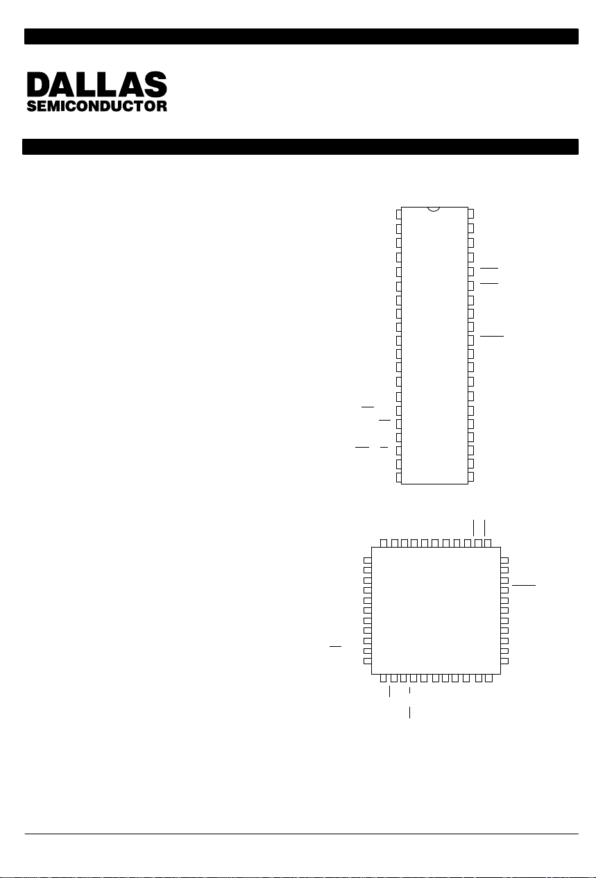
PIN ASSIGNMENT
1
TCLK
2
TSER
AD0
AD1
AD2
AD3
AD4
AD5
AD6
AD7
BTS
RD (DS)
NC
TCHCLK
RD
ALE(AS)
WR
3
TPOS
4
5
TNEG
6
AD0
7
AD1
8
AD2
9
AD3
10
AD4
11
AD5
12
AD6
13
AD7
14
BTS
15
(DS)
16
CS
17
18
(R/W)
19
RLINK
20 21
VSS
40–PIN DIP (600 MIL)
TNEG
TPOS
TCHCLK
7
8
9
10
11
12
44–PIN PLCC
13
14
15
16
17
1819 202122 2324
CS
NC
ALE(AS)
TSER
TCLK
VDD
123456 44 43 42 41 40
VSS
RLINK
WR(R/W)
40
39
38
37
36
35
34
33
32
31
30
29
28
27
26
25
24
23
22
TSYNC
TLINK
TLCLK
25 262728
RCLK
RLCLK
RCHCLK
VDD
TSYNC
TLINK
TLCLK
INT1
INT2
RLOS/LOTC
TCHBLK
RCHBLK
LI_CS
LI_CLK
LI_SDI
SYSCLK
RNEG
RPOS
RSYNC
RSER
RCHCLK
RCLK
RLCLK
INT1
INT2
RLOS/LOTC
39
TCHBLK
38
RCHBLK
37
LI_CS
36
LI_CLK
35
LI_SDI
34
NC
33
NC
32
SYSCLK
31
RNEG
30
RPOS
29
RSER
RSYNC
Copyright 1997 by Dallas Semiconductor Corporation.
All Rights Reserved. For important information regarding
patents and other intellectual property rights, please refer to
Dallas Semiconductor data books.
031397 1/40
Page 2

DS2143/DS2143Q
1.0 INTRODUCTION
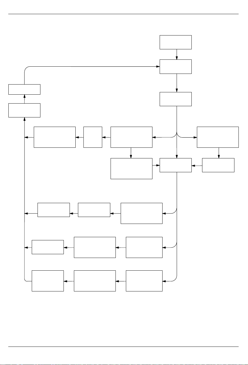
The DS2143 E1 Controller has four main sections: the
receive side, the transmit side, the line interface controller, and the parallel control port. See the Block Diagram.
On the receive side, the device will clock in the serial E1
stream via the RPOS and RNEG pins. The synchronizer will locate the frame and multiframe patterns and
establish their respective positions. This information
will be used by the rest of the receive side circuitry.
The DS2143 is an “off–line” framer , which means that all
of the E1 serial stream that goes into the device, will
come out of it, unchanged. Once the E1 data has been
framed to, the signaling data can be extracted. The
two–frame elastic store can either be enabled or
bypassed.
The transmit side clocks in the unframed E1 stream at
TSER and adds in the framing pattern and the signaling.
The line Interface control port will update line interface
devices that contain a serial port. The parallel control
port contains a multiplexed address and data structure
which can be connected to either a microcontroller or
microprocessor.
Reader’s Note:
This data sheet assumes a particular nomenclature of
the E1 operating environment. There are 32 eight–bit
timeslots in an E1 systems which are number 0 to 31.
Timeslot 0 is transmitted first and received first. These
32 timeslots are also referred to as channels with a numbering scheme of 1 to 32. Timeslot 0 is identical to channel 1, timeslot 1 is identical to channel 2, and so on.
Each timeslot (or channel) is made up of eight bits which
are numbered 1 to 8. Bit number 1 is the MSB and is
transmitted first. Bit number 8 is the LSB and is transmitted last. Throughout this data sheet, the following
abbreviations will be used:
DS2143 FEATURES
• Parallel control port
• Onboard two–frame elastic store
• CAS signaling bit extraction and insertion
• Fully independent transmit and receive sections
• Full alarm detection
• Full access to Si and Sa bits
• Loss of transmit clock detection
• HDB3 coder/decoder
• Full transmit transparency
• Large error counters
• Individual bit–by–bit Sa data link support circuitry
• Programmable output clocks
• Frame sync generation
• Local loopback capability
• Automatic CRC4 E–bit support
• Loss of receive clock detection
• G.802 E1 to T1 mapping support
FAS Frame Alignment Signal
CRC4 Cyclical Redundancy Check
CAS Channel Associated Signaling
CCS Common Channel Signaling
MF Multiframe
Sa Additional bits
Si International bits
E–bit CRC4 Error bits
031397 2/40
Page 3
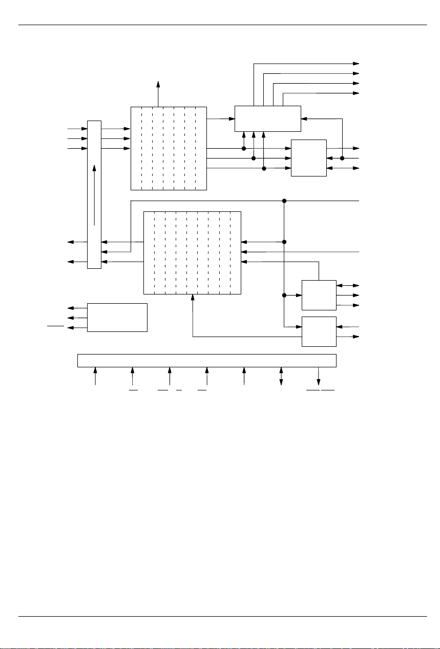
DS2143 BLOCK DIAGRAM
RPOS
RCLK
RNEG
LOCAL LOOPBACK
TPOS
TNEG
LI_SDI
LI_SCLK
LI_CS
LINE INTERFACE
CONTROL PORT
RLOS
RECEIVE SIDE
FRAMER
BPV COUNTER
HDB3 DECODER
SYNCHRONIZER
TRANSMIT SIDE FORMATTER
AIS GENERATION
E–BIT COUNT
ALARM DETECTION
CRC4 ERROR COUNT
SIGNALING EXTRACTION
HDB3 ENCODE
CRC4 GENERATION
IDLE CODE INSERTION
SIGNALING INSERTION
Sa BIT INSERTION
E–BIT INSERTION
Si BIT INSERTION
FAS WORD INSERTION
TIMING CONTROL/
Sa EXTRACTION
ELASTIC
STORE
TIMING
CONTROL
INTERT
LOGIC
DS2143/DS2143Q
RLINK
RLCLK
RCHBLK
RCHCLK
RSER
SYSCLK
RSYNC
TCLK
TSER
TSYNC
TCHCLK
TCHBLK
Sa
TLINK
TLCLK
PARALLEL CONTROL PORT (ROUTED TO ALL BLOCKS)
BTS CS WR(R/W)RD(DS) ALE(AS) AD0–AD7 INT1/INT2
031397 3/40
Page 4
DS2143/DS2143Q
45TPOS
O
Transmit Bipolar Data. Updated on rising edge of TCLK.
2627RPOS
I
Receive Bipolar Data Inputs. Sampled on falling edge of RCLK.
PIN DESCRIPTION Table 1
PIN SYMBOL TYPE DESCRIPTION
1 TCLK I Transmit Clock. 2.048 MHz primary clock. A clock must be applied at the
2 TSER I Transmit Serial Data. Transmit NRZ serial data, sampled on the falling edge
3 TCHCLK O T ransmit Channel Clock. 256 KHz clock which pulses high during the LSB
4 TPOS O Transmit Bipolar Data. Updated on rising edge of TCLK.
TNEG
6–13 AD0–AD7 I/O Address/Data Bus. A 8–bit multiplexed address/data bus.
14 BTS I Bus Type Select. Strap high to select Motorola bus timing; strap low to
15 RD(DS) I Read Input (Data Strobe).
16 CS I Chip Select. Must be low to read or write the port.
17 ALE(AS) I Address Latch Enable (Address Strobe). A positive going edge serves to
18 WR(R/W) I Write Input (Read/Write).
19 RLINK O Receive Link Data. Outputs Sa bits. See Section 13 for timing details.
20 V
SS
21 RLCLK O Receive Link Clock. 4 KHz to 20 KHz demand clock for the RLINK output.
22 RCLK I Receive Clock. 2.048 MHz primary clock. A clock must be applied at the
23 RCHCLK O Receive Channel Clock. 256 KHz clock which pulses high during the LSB
24 RSER O Receive Serial Data. Received NRZ serial data, updated on rising edges
25 RSYNC I/O Receive Sync. An extracted pulse, one RCLK wide, is output at this pin
26 RPOS I Receive Bipolar Data Inputs. Sampled on falling edge of RCLK.
RNEG
28 SYSCLK I System Clock. 1.544 MHz or 2.048 MHz clock. Only used when the elastic
29 LI_SDI O Serial Port Data for the Line Interface. Connects directly to the SDI input
TCLK pin for the parallel port to operate properly.
of TCLK.
of each channel. Useful for parallel to serial conversion of channel data. See
Section 13 for timing details.
For optical links, can be programmed to output NRZ data.
select Intel bus timing. This pin controls the function of the RD
ALE(AS), and WR
(R/W)pins. If BTS=1, then these pins assume the function
listed in parenthesis ().
demultiplex the bus.
– Signal Ground. 0.0 volts.
Controlled by RCR2. See Section 13 for timing details.
RCLK pin for the parallel port to operate properly.
of each channel. Useful for serial to parallel conversion of channel data. See
Section 13 for timing details.
of RCLK.
which indentifies either frame (RCR1.6=0) or multiframe boundaries
(RCR1.6=1). If the elastic store is enabled via the RCR2.1, then this pin can
be enabled to be an input via RCR1.5 at which a frame boundary pulse is
applied. See Section 13 for timing details.
Tie together to receive NRZ data and disable BPV monitoring circuitry.
store function is enabled via the RCR2.1. Should be tied low in applications
that do not use the elastic store.
pin on the line interface. See Sections 12 and 13 for timing details.
(DS),
031397 4/40
Page 5
DS2143/DS2143Q
pp
PIN DESCRIPTIONTYPESYMBOL
30 LI_CLK O Serial Port Clock for the Line Interface. Connects directly to the SCLK
input pin on the line interface. See Sections 12 and 13 for timing details.
31 LI_CS O Serial Port Chip Select for the Line Interface. Connects directly to the CS
input pin on the line interface. See Sections 12 and 13 for timing details.
32
33
RCHBLK
TCHBLK
O Receive/Transmit Channel Block. A user programmable output that can
be forced high or low during any of the 32 E1 channels. Useful for blocking
clocks to a serial UART or LAPD controller in applications where not all E1
channels are used such as Fractional E1 or ISDN–PRI. Also useful for locating individual channels in drop–and–insert applications. See Sections 9 and
13 for details.
34 RLOS/LOTC O Receive Loss of Sync/Loss of Transmit Clock. A dual function output.
If TCR2.0=0, then this pin will toggle high when the synchronizer is searching
for the E1 frame and multiframe. If TCR2.0=1, then this pin will toggle high
if the TCLK pin has not toggled for 5 µs.
35 INT2 O Receive Alarm Interrupt 2. Flags host controller during conditions defined
in Status Register 2. Active low, open drain output.
36 INT1 O Receive Alarm Interrupt 1. Flags host controller during alarm conditions
defined in Status Register 1. Active low, open drain output.
37 TLCLK O Transmit Link Clock. 4 KHz to 20 KHz demand clock for the TLINK input.
Controlled by TCR2. See Section 13 for timing details.
38 TLINK I T ransmit Link Data. If enabled, this pin will be sampled on the falling edge
of TCLK to insert Sa bits. See Section 13 for timing details.
39 TSYNC I/O Transmit Sync. A pulse at this pin will establish either frame or CAS multi-
frame boundaries for the DS2143. Via TCR1.1, the DS2143 can be programmed to output either a frame or multiframe pulse at this pin. See Section
13 for timing details.
40 VDD – Positive Supply. 5.0 volts.
031397 5/40
Page 6
DS2143/DS2143Q
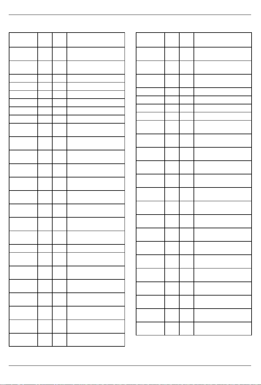
DS2143 REGISTER MAP
ADDRESS
A7 to A0
00000000 00 R Bipolar Violation Count
00000001 01 R Bipolar Violation Count
00000010 02 R CRC4 Count Register 1.
00000011 03 R CRC4 Count Register 2.
00000100 04 R E–Bit Count Register 1.
00000101 05 R E–Bit Count Register 2.
000001 10 06 R/W Status Register 1.
000001 11 07 R/W Status Register 2.
00001000 08 R/W Receive Information
0001 11 10 1E R Synchronizer Status
000101 10 16 R/W Interrupt Mask
000101 11 17 R/W Interrupt Mask
00010000 10 R/W Receive Control
00010001 11 R/W Receive Control
00010010 12 R/W Transmit Control
0001001 1 13 R/W Transmit Control
00010100 14 R/W Common Control
00010101 15 R/W Test Register.
0001 1000 18 W LI Control Register Byte
0001 1001 19 W LI Control Register Byte
00100000 20 R/W Transmit Align Frame
00100001 21 R/W Transmit Non–Align
00101 111 2F R Receive Align Frame
0001 1111 1F R Receive Non–Align
00100010 22 R/W Transmit Channel Block-
HEX R/W REGISTER NAME
Register 1.
Register 2.
Register.
Register.
Register 1.
Register 2.
Register 1.
Register 2.
Register 1.
Register 2.
Register.
1.
2.
Register.
Frame Register.
Register.
Frame Register.
ing Register 1.
ADDRESS
HEX R/W REGISTER NAME
A7 to A0
00100011 23 R/W Transmit Channel Block-
ing Register 2.
00100100 24 R/W Transmit Channel Block-
ing Register 3.
00100101 25 R/W Transmit Channel Block-
ing Register 4.
001001 10 26 R/W Transmit Idle Register 1.
001001 11 27 R/W Transmit Idle Register 2.
00101000 28 R/W Transmit Idle Register 3.
00101001 29 R/W Transmit Idle Register 4.
00101010 2A R/W Transmit Idle Definition
Register.
0010101 1 2B R/W Receive Channel Block-
ing Register 1.
00101 100 2C R/W Receive Channel Block-
ing Register 2.
00101 101 2D R/W Receive Channel Block-
ing Register 3.
00101 110 2E R/W Receive Channel Block-
ing Register 4.
00110000 30 R Receive Signaling
Register 1.
00110001 31 R Receive Signaling
Register 2.
00110010 32 R Receive Signaling
Register 3.
00110011 33 R Receive Signaling
Register 4.
00110100 34 R Receive Signaling
Register 5.
00110101 35 R Receive Signaling
Register 6.
00110110 36 R Receive Signaling
Register 7.
00110111 37 R Receive Signaling
Register 8.
00111000 38 R Receive Signaling
Register 9.
00111001 39 R Receive Signaling
Register 10.
00111010 3A R Receive Signaling
Register 11.
031397 6/40
Page 7
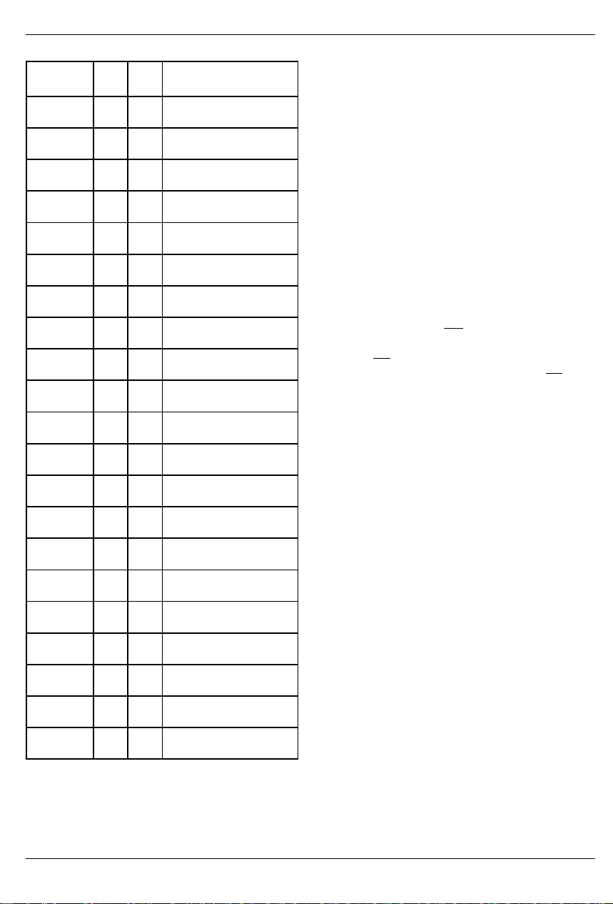
DS2143/DS2143Q
ADDRESS
HEX R/W REGISTER NAME
A7 to A0
00111011 3B R Receive Signaling
Register 12.
00111100 3C R Receive Signaling
Register 13.
00111101 3D R Receive Signaling
Register 14.
00111110 3E R Receive Signaling
Register 15.
00111111 3F R Receive Signaling
Register 16.
01000000 40 R/W Transmit Signaling
Register 1.
01000001 41 R/W Transmit Signaling
Register 2.
01000010 42 R/W Transmit Signaling
Register 3.
0100001 1 43 R/W Transmit Signaling
Register 4.
01000100 44 R/W Transmit Signaling
Register 5.
01000101 45 R/W Transmit Signaling
Register 6.
010001 10 46 R/W Transmit Signaling
Register 7.
010001 11 47 R/W Transmit Signaling
Register 8.
01001000 48 R/W Transmit Signaling
Register 9.
01001001 49 R/W Transmit Signaling
Register 10.
01001010 4A R/W Transmit Signaling
Register 11.
0100101 1 4B R/W Transmit Signaling
Register 12.
01001 100 4C R/W Transmit Signaling
Register 13.
01001 101 4D R/W Transmit Signaling
Register 14.
01001 110 4E R/W Transmit Signaling
Register 15.
01001 111 4F R/W Transmit Signaling
Register 16.
2.0 PARALLEL PORT
The DS2143 is controlled via a mutliplexed bidirectional
address/data bus by an external microcontroller or
microprocessor. The DS2143 can operate with either
Intel or Motorola bus timing configurations. If the BTS
pin is tied low, Intel timing will be selected; if tied high,
Motorola timing will be selected. All Motorola bus signals are listed in parenthesis (). See the timing diagrams in the AC Electrical Characteristics for more
details. The mutliplexed bus on the DS2143 saves pins
because the address information and data information
share the same signal paths. The addresses are presented to the pins in the first portion of the bus cycle and
data will be transferred on the pins during second portion of the bus cycle. Addresses must be valid prior to
the falling edge of ALE(AS), at which time the DS2143
latches the address from the AD0 to AD7 pins. Valid
write data must be present and held stable during the
later portion of the DS or WR
pulses. In a read cycle, the
DS2143 outputs a byte of data during the latter portion of
the DS or RD pulses. The read cycle is terminated and
the bus returns to a high impedance state as RD transitions high in Intel timing or as DS transitions low in Motorola timing.
3.0 CONTROL AND TEST REGISTERS
The operation of the DS2143 is configured via a set of
five registers. Typically, the control registers are only
accessed when the system is first powered up. Once
the DS2143 has been initialized, the control registers
will only need to be accessed when there is a change in
the system configuration. There are two Receive Control Registers (RCR1 and RCR2), two Transmit Control
Registers (TCR1 and TCR2), and a Common Control
Register (CCR). Each of the five registers are described
in this section.
The T est Register at address 15 hex is used by the factory in testing the DS2143. On power–up, the T est Register should be set to 00 hex in order for the DS2143 to
operate properly .
031397 7/40
Page 8

DS2143/DS2143Q
RCR1: RECEIVE CONTROL REGISTER 1 (Address=10 Hex)
(MSB) (LSB)
RSMF RSM RSIO – – FRC SYNCE RESYNC
SYMBOL POSITION NAME AND DESCRIPTION
RSMF RCR1.7 RSYNC Multiframe Function. Only used if the RSYNC pin is pro-
RSM RCR1.6 RSYNC Mode Select.
RSIO RCR1.5 RSYNC I/O Select.
– RCR1.4 Not Assigned. Should be set to zero when written to.
– RCR1.3 Not Assigned. Should be set to zero when written to.
FRC RCR1.2 Frame Resync Criteria.
SYNCE RCR1.1 Sync Enable.
RESYNC RCR1.0 Resync. When toggled from low to high, a resync is initiated. Must be
grammed in the multiframe mode (RCR1.6=1).
0 = RSYNC outputs CAS multiframe boundaries
1 = RSYNC outputs CRC4 multiframe boundaries
0 = frame mode (see the timing in Section 13)
1 = multiframe mode (see the timing in Section 13)
0 = RSYNC is an output (depends on RCR1.6)
1 = RSYNC is an input (only valid if elastic store enabled) (note: this bit must
be set to zero when RCR2.1=0)
0 = resync if FAS received in error 3 consecutive times
1 = resync if FAS or bit 2 of non–F AS is received in error 3 consecutive times
0 = auto resync enabled
1 = auto resync disabled
cleared and set again for a subsequent resync.
SYNC/RESYNC CRITERIA Table 2
FRAME OR
MULTIFRAME
LEVEL
FAS FAS present in frames N and N +
CRC4 Two valid MF alignment words
CAS Valid MF alignment word found
031397 8/40
SYNC CRITERIA RESYNC CRITERIA ITU SPEC.
2, and FAS not present in frame
N + 1.
found within 8 ms.
and previous time slot 16 contains code other than all zeros.
Three consecutive incorrect FAS
received.
Alternate (RCR1.2=1) the above
criteria is met or three consecutive incorrect bit 2 of non–FAS
received.
915 or more CRC4 code words
out of 1000 received in error.
Two consecutive MF alignment
words received in error.
G.706
4.1.1
4.1.2
G.706
4.2
4.3.2
G.732
5.2
Page 9

DS2143/DS2143Q
RCR2: RECEIVE CONTROL REGISTER 2 (Address=11 Hex)
(MSB) (LSB)
Sa8S Sa7S Sa6S Sa5S Sa4S SCLKM ESE –
SYMBOL POSITION NAME AND DESCRIPTION
Sa8S RCR2.7 Sa8 Bit Select. Set to one to report the Sa8 bit at the RLINK pin; set to zero
Sa7S RCR2.6 Sa7 Bit Select. Set to one to report the Sa7 bit at the RLINK pin; set to zero
Sa6S RCR2.5 Sa6 Bit Select. Set to one to report the Sa6 bit at the RLINK pin; set to zero
Sa5S RCR2.4 Sa5 Bit Select. Set to one to report the Sa5 bit at the RLINK pin; set to zero
Sa4S RCR2.3 Sa4 Bit Select. Set to one to report the Sa4 bit at the RLINK pin; set to zero
SCLKM RCR2.2 SYSCLK Mode Select.
ESE RCR2.1 Elastic Store Enable.
– RCR2.0 Not Assigned. Should be set to zero when written to.
to not report the Sa8 bit.
to not report the Sa7 bit.
to not report the Sa6 bit.
to not report the Sa5 bit.
to not report the Sa4 bit.
0 = if SYSCLK is 1.544 MHz
1 = if SYSCLK is 2.048 MHz
0 = elastic store is bypassed
1 = elastic store is enabled
TCR1: TRANSMIT CONTROL REGISTER 1 (Address=12 Hex)
(MSB) (LSB)
ODF
SYMBOL POSITION NAME AND DESCRIPTION
ODF TCR1.7 Output Data Format.
TFPT TCR1.6 Transmit Timeslot 0 Pass Through.
T16S TCR1.5 Transmit Timeslot 16 Data Select.
TUA1 TCR1.4 Transmit Unframed All Ones.
TSiS TCR1.3 Transmit International Bit Select.
TFPT T16S TUA1 TSiS TSA1 TSM TSIO
0 = bipolar data at TPOS and TNEG
1 = NRZ data at TPOS; TNEG=0
0 = FAS bits/Sa bits/Remote Alarm sourced internally from the TAF and
TNAF registers
1 = FAS bits/Sa bits/Remote Alarm sourced from TSER
0 = sample timeslot 16 at TSER pin
1 = source timeslot 16 from TS1 to TS16 registers
0 = transmit data normally
1 = transmit an unframed all one’s code at TPOS and TNEG
0 = sample Si bits at TSER pin
1 = source Si bits from TAF and TNAF registers (in this mode, TCR1.6 must
be set to 0)
031397 9/40
Page 10

DS2143/DS2143Q
TSA1 TCR1.2 Transmit Signaling All Ones.
0 = normal operation
1 = force timeslot 16 in every frame to all ones
TSM TCR1.1 TSYNC Mode Select.
0 = frame mode (see the timing in Section 13)
1 = CAS and CRC4 multiframe mode (see the timing in Section 13)
TSIO TCR1.0 TSYNC I/O Select.
0 = TSYNC is an input
1 = TSYNC is an output
TCR2: TRANSMIT CONTROL REGISTER 2 (Address=13 Hex)
(MSB) (LSB)
Sa8S
SYMBOL POSITION NAME AND DESCRIPTION
Sa8S TCR2.7 Sa8 Bit Select. Set to one to source the Sa8 bit from the TLINK pin; set to
Sa7S TCR2.6 Sa7 Bit Select. Set to one to source the Sa7 bit from the TLINK pin; set to
Sa6S TCR2.5 Sa6 Bit Select. Set to one to source the Sa6 bit from the TLINK pin; set to
Sa5S TCR2.4 Sa5 Bit Select. Set to one to source the Sa5 bit from the TLINK pin; set to
Sa4S TCR2.3 Sa4 Bit Select. Set to one to source the Sa4 bit from the TLINK pin; set to
– TCR2.2 Not Assigned. Should be set to zero when written to.
AEBE TCR2.1 Automatic E–Bit Enable.
P34F TCR2.0 Function of Pin 34.
Sa7S Sa6S Sa5S Sa4S – AEBE P34F
zero to not source the Sa8 bit.
zero to not source the Sa7 bit.
zero to not source the Sa6 bit.
zero to not source the Sa5 bit.
zero to not source the Sa4 bit.
0 = E–bits not automatically set in the transmit direction
1 = E–bits automatically set in the transmit direction
0 = Receive Loss of Sync (RLOS)
1 = Loss of Transmit Clock (LOTC)
CCR: COMMON CONTROL REGISTER (Address=14 Hex)
(MSB) (LSB)
LLB
SYMBOL POSITION NAME AND DESCRIPTION
LLB CCR.7 Local Loopback.
THDB3 CCR.6 Transmit HDB3 Enable.
031397 10/40
THDB3 TG802 TCRC4 RSM RHDB3 RG802 RCRC4
0 = loopback disabled
1 = loopback enabled
0 = HDB3 disabled
1 = HDB3 enabled
Page 11

DS2143/DS2143Q
TG802 CCR.5 T ransmit G.802 Enable. See Section 13 for details.
0 = do not force TCHBLK high during bit 1 of timeslot 26
1 = force TCHBLK high during bit 1 of timeslot 26
TCRC4 CCR.4 Transmit CRC4 Enable.
0 = CRC4 disabled
1 = CRC4 enabled
RSM CCR.3 Receive Signaling Mode Select.
0 = CAS signaling mode
1 = CCS signaling mode
RHDB3 CCR.2 Receive HDB3 Enable.
0 = HDB3 disabled
1 = HDB3 enabled
RG802 CCR.1 Receive G.802 Enable. See Section 13 for details.
0 = do not force RCHBLK high during bit 1 of timeslot 26
1 = force RCHBLK high during bit 1 of timeslot 26
RCRC4 CCR.0 Receive CRC4 Enable.
0 = CRC4 disabled
1 = CRC4 enabled
LOCAL LOOPBACK
When CCR.7 is set to a one, the DS2143 will enter a
Local LoopBack (LLB) mode. This loopback is useful in
testing and debugging applications. In LLB, the
DS2143 will loop data from the transmit side back to the
receive side. This loopback is synonymous with replacing the RCLK input with the TCLK signal, and the RPOS/
RNEG inputs with the TPOS/TNEG outputs. When LLB
is enabled, the following will occur;
The user will always precede a read of the SR1, SR2,
and RIR registers with a write. The byte written to the
register will inform the DS2143 which bits the user
wishes to read and have cleared. The user will write a
byte to one of these three registers, with a one in the bit
positions he or she wishes to read and a zero in the bit
positions he or she does not wish to obtain the latest
information on. When a one is written to a bit location,
the read register will be updated with current value and it
will be cleared. When a zero is written to a bit position,
1. data at RPOS and RNEG will be ignored
2. all receive side signals will take on timing synchronous with TCLK instead of RCLK
3. all functions are available.
4.0 STATUS AND INFORMATION REGISTERS
There is a set of four registers that contain information
on the current real time status of the DS2143, Status
Register 1 (SR1), Status Register 2 (SR2), Receive
Information Register (RIR), and Synchronizer Status
Register (SSR). When a particular event has occurred
(or is occurring), the appropriate bit in one of these three
registers will be set to a one. All of the bits in these registers operate in a latched fashion (except for the SSR).
This means that if an event occurs and a bit is set to a
one in any of the registers, it will remain set until the user
reads that bit. The bit will be cleared when it is read and
it will not be set again until the event has occurred again
or if the alarm(s) is still present.
the read register will not be updated and the previous
value will be held. A write to the status and information
registers will be immediately followed by a read of the
same register. The read result should be logically
AND’ed with the mask byte that was just written and this
value should be written back into the same register to
insure that the bit does indeed clear. This second write
is necessary because the alarms and events in the status registers occur asynchronously in respect to their
access via the parallel port. This scheme allows an
external microcontroller or microprocessor to individually poll certain bits without disturbing the other bits in
the register. This operation is key in controlling the
DS2143 with higher order software languages.
The SSR register operates differently than the other
three. It is a read only register and it reports the status of
the synchronizer in real time. This register is not latched
and it is not necessary to precede a read of this registers
with a write.
031397 11/40
Page 12

DS2143/DS2143Q
The SR1 and SR2 registers have the unique ability to
initiate a hardware interrupt via the INT1
and INT2 pins
respectively. Each of the alarms and events in the SR1
and SR2 can be either masked or unmasked from the
interrupt pins via the Interrupt Mask Register 1 (IMR1)
and Interrupt Mask Register 2 (IMR2) respectively.
RIR: RECEIVE INFORMATION REGISTER (Address=08 Hex)
(MSB) (LSB)
–
– – ESF ESE – FASRC CASRC
SYMBOL POSITION NAME AND DESCRIPTION
– RIR.7 Not Assigned. Could be any value when read.
– RIR.6 Not Assigned. Could be any value when read.
– RIR.5 Not Assigned. Could be any value when read.
ESF RIR.4 Elastic Store Full. Set when the elastic store buffer fills and a frame is
deleted.
ESE RIR.3 Elastic Store Empty. Set when the elastic store buffer empties and a
frame is repeated.
– RIR.2 Not Assigned. Could be any value when read.
FASRC RIR.1 FAS Resync Criteria Met. Set when three consecutive FAS words are
received in error.
CASRC RIR.0 CAS Resync Criteria Met. Set when two consecutive CAS MF alignment
words are received in error.
SSR: SYNCHRONIZER STATUS REGISTER (Address=1E Hex)
(MSB) (LSB)
CSC5 CSC4 CSC3 CSC2 CSC0 FASSA CASSA CRC4SA
SYMBOL POSITION NAME AND DESCRIPTION
CSC5 SSR.7 CRC4 Sync Counter Bit 5. MSB of the 6–bit counter.
CSC4 SSR.6 CRC4 Sync Counter Bit 4.
CSC3 SSR.5 CRC4 Sync Counter Bit 3.
CSC2 SSR.4 CRC4 Sync Counter Bit 2.
CSC1 SSR.3 CRC4 Sync Counter Bit 0. LSB of the 6–bit counter. The next to LSB is not
accessible.
FASSA SSR.2 F AS Sync Active. Set while the synchronizer is searching for alignment at
the FAS level.
CASSA SSR.1 CAS MF Sync Active. Set while the synchronizer is searching for the CAS
MF alignment word.
CRC4SA SSR.0 CRC4 MF Sync Active. Set while the synchronizer is searching for the
CRC4 MF alignment word.
031397 12/40
Page 13

DS2143/DS2143Q
CRC4 SYNC COUNTER
The CRC4 Sync Counter increments each time the 8ms
CRC4 multiframe search times out. The counter is
cleared when the DS2143 has successfully obtained
synchronization at the CRC4 level. The counter can
also be cleared by disabling the CRC4 mode
amount of time the DS2143 has been searching for synchronization at the CRC4 level. Annex B of CCITT
G.706 suggests that if synchronization at the CRC4
level cannot be obtained within 400 ms, then the search
should be abandoned and proper action taken. The
CRC4 Sync Counter will rollover.
(CCR.0=0). This counter is useful for determining the
SR1: STATUS REGISTER 1 (Address=06 Hex)
(MSB) (LSB)
RSA1
SYMBOL POSITION NAME AND DESCRIPTION
RSA1 SR1.7 Receive Signaling All Ones. Set when the contents of timeslot 16 con-
RDMA SR1.6 Receive Distant MF Alarm. Set when bit 6 of timeslot 16 in frame 0 has
RSA0 SR1.5 Receive Signaling All Zeros. Set when over a full MF, timeslot 16 con-
SLIP SR1.4 Elastic Store Slip Occurrence. Set when the elastic store has either
RUA1 SR1.3 Receive Unframed All Ones. Set when an unframed all ones code is
RRA SR1.2 Receive Remote Alarm. Set when a remote alarm is received at RPOS
RCL SR1.1 Receive Carrier Loss. Set when 255 consecutive zeros have been
RLOS SR1.0 Receive Loss of Sync. Set when the device is not synchronized to the
RDMA RSA0 SLIP RUA1 RRA RCL RLOS
tains less than 3 zeros over 16 consecutive frames. This alarm is not disabled in the CCS signaling mode.
been set for 2 consecutive multiframes. This alarm is not disabled in the
CCS signaling mode.
tains all zeros.
repeated or deleted a frame of data.
received at RPOS and RNEG.
and RNEG.
detected at RPOS and RNEG.
receive E1 stream.
031397 13/40
Page 14

DS2143/DS2143Q
ALARM CRITERIA Table 3
ALARM SET CRITERIA CLEAR CRITERIA
RSA1
(receive signaling
all ones)
RSA0
(receive signaling
all zeros)
RDMA
(receive distant
over 16 consecutive frames (one full
MF) timeslot 16 contains less than 3
zeros
over 16 consecutive frames (one full
MF) timeslot 16 contains all zeros
bit 6 in timeslot 16 of frame 0 set to
one for two consecutive MF
over 16 consecutive frames (one full
MF) timeslot 16 contains 3 or more
zeros
over 16 consecutive frames (one full
MF) timeslot 16 contains at least a
single one
bit 6 in timeslot 16 of frame 0 set to
zero for a two consecutive MF
multiframe alarm)
RUA1
(receive unframed
less than 3 zeros in two frames (512
bits)
more than 2 zeros in two frames (512
bits)
all ones)
RRA
(receive remote
bit 3 of non–align frame set to one for
3 consecutive occasions
bit 3 of non–align frame set to zero for
3 consecutive occasions
alarm)
RCL
(receive carrier
255 consecutive zeros received in 255 bit times, at least 32 ones are
received
loss)
Note: all the alarm bits in Status Register 1 except the RUA1 will remain set after they are read if the alarm condition
still exists; the RUA1 will clear and check the next 512 bits for an all one’s condition at which point it will again be set if
the alarm condition still is present.
ITU
SPEC.
G.732
4.2
G.732
5.2
O.162
2.1.5
O.162
1.6.1.2
O.162
2.1.4
G.775
SR2: STATUS REGISTER 2 (Address=07 Hex)
(MSB) (LSB)
RMF RAF TMF SEC TAF LOTC RCMF LORC
SYMBOL POSITION NAME AND DESCRIPTION
RMF SR2.7 Receive CAS Multiframe. Set every 2 ms (regardless if CAS signaling is
RAF SR2.6 Receive Align Frame. Set every 250 µs at the beginning of align frames.
TMF SR2.5 Transmit Multiframe. Set every 2 ms (regardless if CRC4 is enabled) on
SEC SR2.4 One Second Timer. Set on increments of one second based on RCLK.
TAF SR2.3 T ransmit Align Frame. Set every 250 µs at the beginning of align frames.
031397 14/40
enabled or not) on receive multiframe boundaries. Used to alert the host
that signaling data is available.
Used to alert the host that Si and Sa bits are available in the RAF and RNAF
registers.
transmit multiframe boundaries. Used to alert the host that signaling data
needs to be updated.
Used to alert the host that the TAF and TNAF registers need to be updated.
Page 15

DS2143/DS2143Q
LOTC SR2.2 Loss of Transmit Clock. Set when the TCLK pin has not transitioned for
one channel time (or 3.9 µs). Will force pin 34 high if enabled via TCR2.0.
Based on RCLK.
RCMF SR2.1 Receive CRC4 Multiframe. Set on CRC4 multiframe boundaries; will con-
tinue to be set every 2 ms on an arbitrary boundary if CRC4 is disabled.
LORC SR2.0 Loss of Receive Clock. Set when the RCLK pin has not transitioned for at
least 2 µs (3 µs ±1 µs).
IMR1: INTERRUPT MASK REGISTER 1 (Address=16 Hex)
(MSB) (LSB)
RSA1 RDMA RSA0 SLIP RUA1 RRA RCL RLOS
SYMBOL POSITION NAME AND DESCRIPTION
RSA1 IMR1.7 Receive Signaling All Ones.
RDMA IMR1.6 Receive Distant MF Alarm.
RSA0 IMR1.5 Receive Signaling All Zeros.
SLIP IMR1.4 Elastic Store Slip Occurrence.
RUA1 IMR1.3 Receive Unframed All Ones.
RRA IMR1.2 Receive Remote Alarm.
RCL IMR1.1 Receive Carrier Loss.
RLOS IMR1.0 Receive Loss of Sync.
0 = interrupt masked
1 = interrupt enabled
0 = interrupt masked
1 = interrupt enabled
0 = interrupt masked
1 = interrupt enabled
0 = interrupt masked
1 = interrupt enabled
0 = interrupt masked
1 = interrupt enabled
0 = interrupt masked
1 = interrupt enabled
0 = interrupt masked
1 = interrupt enabled
0 = interrupt masked
1 = interrupt enabled
031397 15/40
Page 16

DS2143/DS2143Q
IMR2: INTERRUPT MASK REGISTER 2 (Address=17 Hex)
(MSB) (LSB)
RMF RAF TMF SEC TAF LOTC RCMF LORC
SYMBOL POSITION NAME AND DESCRIPTION
RMF IMR2.7 Receive CAS Multiframe.
RAF IMR2.6 Receive Align Frame.
TMF IMR2.5 Transmit Multiframe.
SEC IMR2.4 One Second Timer.
TAF IMR2.3 Transmit Align Frame.
LOTC IMR2.2 Loss Of Transmit Clock.
RCMF IMR2.1 Receive CRC4 Multiframe.
LORC IMR2.0 Loss of Receive Clock.
0 = interrupt masked
1 = interrupt enabled
0 = interrupt masked
1 = interrupt enabled
0 = interrupt masked
1 = interrupt enabled
0 = interrupt masked
1 = interrupt enabled
0 = interrupt masked
1 = interrupt enabled
0 = interrupt masked
1 = interrupt enabled
0 = interrupt masked
1 = interrupt enabled
0 = interrupt masked
1 = interrupt enabled
5.0 ERROR COUNT REGISTERS
There are a set of three counters in the DS2143 that
record bipolar violations, errors in the CRC4 SMF code
words, and E–bits as reported by the far end. Each of
these three counters are automatically updated on one
second boundaries as determined by the one second
timer in Status Register 2 (SR2.4). Hence, these regis-
031397 16/40
ters contain performance data from the previous
second. The user can use the interrupt from the one
second timer to determine when to read these registers.
The user has a full second to read the counters before
the data is lost.
Page 17
BPVCR1: UPPER BIPOLAR VIOLATION COUNT REGISTER 1 (Address=00 Hex)
BPVCR2: LOWER BIPOLAR VIOLATION COUNT REGISTER 2 (Address=01 Hex)
(MSB) (LSB)
BV7
BV15 BV14 BV13 BV12 BV11 BV10 BV9 BV8
SYMBOL POSITION NAME AND DESCRIPTION
BV15 BPVCR1.7 MSB of the bipolar violation count
Bipolar Violation Count Register 1 (BPVCR1) is the
most significant word and BPVCR2 is the least significant word of a 16–bit counter that records bipolar violations (BPVs). If the HDB3 mode is set for the receive
side via CCR.2, then HDB3 code words are not counted.
BV6 BV5 BV4 BV3 BV2 BV1 BV0
BV0 BPVCR2.0 LSB of the bipolar violation count
This counter increments at all times and is not disabled
by loss of sync conditions. The counter saturates at
65,535 and will not rollover. The bit error rate on a E1
line would have to be greater than 10**–2 before the
BPVCR would saturate.
CRCCR1: CRC4 COUNT REGISTER 1 (Address=02 Hex)
CRCCR2: CRC4 COUNT REGISTER 2 (Address=03 Hex)
(MSB) (LSB)
CRC7 CRC6 CRC5 CRC4 CRC3 CRC2 CRC1 CRC0
CRC14 CRC14 CRC13 CRC12 CRC11 CRC10 CRC9 CRC8
DS2143/DS2143Q
BPVCR2
BPVCR1
CRCCR2
CRCCR1
SYMBOL POSITION NAME AND DESCRIPTION
CRC15 CRCCR1.7 MSB of the CRC4 error count
CRC0 CRCCR2.0 LSB of the CRC4 error count
CRC4 Count Register 1 (CRCCR1) is the most significant word and CRCCR2 is the least significant word of a
16–bit counter that records word errors in the Cyclic
Redundancy Check 4 (CRC4). Since the maximum
CRC4 count in a one second period is 1000, this counter
cannot saturate. The counter is disabled during loss of
sync at either the FAS or CRC4 level; it will continue to
count if loss of sync occurs at the CAS level.
EBCR1: E–BIT COUNT REGISTER 1 (Address=04 Hex)
EBCR2: E–BIT COUNT REGISTER 2 (Address=05 Hex)
(MSB) (LSB)
EB7 EB6 EB5 EB4 EB3 EB2 EB1 EB0
EB15 EB14 EB13 EB12 EB11 EB10 EB9 EB8
SYMBOL POSITION NAME AND DESCRIPTION
EB15 EBCR1.7 MSB of the E–Bit error count
EB0 EBCR2.0 LSB of the E–Bit error count
E–bit Count Register 1 (EBCR1) is the most significant
word and EBCR2 is the least significant word of a 16–bit
counter that records Far End Block Errors (FEBE) as
reported in the first bit of frames 13 and 15 on E1 lines
running with CRC4 multiframe. These count registers
will increment once each time the received E–bit is set to
zero. Since the maximum E–bit count in a one second
period is 1000, this counter cannot saturate. The
counter is disabled during loss of sync at either the FAS
EBCR2
EBCR1
031397 17/40
Page 18

DS2143/DS2143Q
or CRC4 level; it will continue to count if loss of sync
occurs at the CAS level.
6.0 Sa DATA LINK CONTROL AND
OPERATION
The DS2143 provides for access to the proposed E1
performance monitor data link in the Sa bit positions.
The device allows access to the Sa bits either via a set of
two internal registers (RNAF and TNAF) or via two
external pins (RLINK and TLINK).
On the receive side, the Sa bits are always reported in
the internal RNAF register (see Section 11 for more
details). All five Sa bits are always output at the RLINK
pin. See Section 13 for detailed timing. Via RCR2, the
user can control the RLCLK pin to pulse during any combination of Sa bits. This allows the user to create a clock
that can be used to capture the needed Sa bits.
On the transmit side, the individual Sa bits can be either
sourced from the internal TNAF register (TCR1.6=0) or
from the external TLINK pin. Via TCR2, the DS2143
can be programmed to source any combination of the
additional bits from the TLINK pin. If the user wishes to
pass the Sa bits through the DS2143 without them being
altered, then the device should be set up to source all
five Sa bits via the TLINK pin and the TLINK pin should
be tied to the TSER pin. Please see the timing diagrams
and the transmit data flow diagram in Section 13 for
examples.
7.0 SIGNALING OPERATION
The Channel Associated Signaling (CAS) bits
embedded in the E1 stream can be extracted from the
receive stream and inserted into the transmit stream by
the DS2143. Each of the 30 channels has four signaling
bits (A/B/C/D) associated with it. The numbers in parenthesis () are the channel associated with a particular
signaling bit. The channel numbers have been
assigned as described in the CCITT documents. For
example, channel 1 is associated with timeslot 1 and
channel 30 is associated with timeslot 31. There is a set
of 16 registers for the receive side (RS1 to RS16) and 16
registers on the transmit side (TS1 to TS16). The
signaling registers are detailed below.
RS1 TO RS16: RECEIVE SIGNALING REGISTERS (Address=30 to 3F Hex)
(MSB) (LSB)
0 0 0 0 X Y X X
A(1) B(1) C(1) D(1) A(16) B(16) C(16) D(16)
A(2) B(2) C(2) D(2) A(17) B(17) C(17) D(17)
A(3) B(3) C(3) D(3) A(18) B(18) C(18) D(18)
A(4) B(4) C(4) D(4) A(19) B(19) C(19) D(19)
A(5) B(5) C(5) D(5) A(20) B(20) C(20) D(20)
A(6) B(6) C(6) D(6) A(21) B(21) C(21) D(21)
A(7) B(7) C(7) D(7) A(22) B(22) C(22) D(22)
A(8) B(8) C(8) D(8) A(23) B(23) C(23) D(23)
A(9) B(9) C(9) D(9) A(24) B(24) C(24) D(24)
A(10) B(10) C(10) D(10) A(25) B(25) C(25) D(25)
A(11) B(11) C(1 1) D(11) A(26) B(26) C(26) D(26)
A(12) B(12) C(12) D(12) A(27) B(27) C(27) D(27)
A(13) B(13) C(13) D(13) A(28) B(28) C(28) D(28)
A(14) B(14) C(14) D(14) A(29) B(29) C(29) D(29)
A(15) B(15) C(15) D(15) A(30) B(30) C(30) D(30)
RS1 (30)
RS2 (31)
RS3 (32)
RS4 (33)
RS5 (34)
RS6 (35)
RS7 (36)
RS8 (37)
RS9 (38)
RS10 (39)
RS11 (3A)
RS12 (3B)
RS13 (3C)
RS14 (3D)
RS15 (3E)
RS16 (3F)
031397 18/40
Page 19

SYMBOL POSITION NAME AND DESCRIPTION
X RS1.0/1/3 Spare Bits
Y RS1.2 Remote Alarm Bit (integrated and reported in SR1.6)
A(1) RS2.7 Signaling Bit A for Channel 1
D(30) RS16.0 Signaling Bit D for Channel 30
Each Receive Signaling Register (RS1 to RS16) reports
the incoming signaling from two timeslots. The bits in
the Receive Signaling Registers are updated on multiframe boundaries so the user can utilize the Receive
Multiframe Interrupt in the Receive Status Register 2
(SR2.7) to know when to retrieve the signaling bits. The
user has a full 2 ms to retrieve the signaling bits before
conditions. Their validity should be qualified by checking for synchronization at the CAS level. In CCS signaling mode, RS1 to RS16 can also be used to extract
signaling information. Via the SR2.7 bit, the user will be
informed when the signaling registers have been loaded
with data. The user has 2 ms to retrieve the data before
it is lost.
the data is lost. The RS registers are updated under all
TS1 TO TS16: TRANSMIT SIGNALING REGISTERS (Address=40 to 4F Hex)
(MSB) (LSB)
0
A(1) B(1) C(1) D(1) A(16) B(16) C(16) D(16)
A(2) B(2) C(2) D(2) A(17) B(17) C(17) D(17)
A(3) B(3) C(3) D(3) A(18) B(18) C(18) D(18)
A(4) B(4) C(4) D(4) A(19) B(19) C(19) D(19)
A(5) B(5) C(5) D(5) A(20) B(20) C(20) D(20)
A(6) B(6) C(6) D(6) A(21) B(21) C(21) D(21)
A(7) B(7) C(7) D(7) A(22) B(22) C(22) D(22)
A(8) B(8) C(8) D(8) A(23) B(23) C(23) D(23)
A(9) B(9) C(9) D(9) A(24) B(24) C(24) D(24)
A(10) B(10) C(10) D(10) A(25) B(25) C(25) D(25)
A(11) B(11) C(1 1) D(11) A(26) B(26) C(26) D(26)
A(12) B(12) C(12) D(12) A(27) B(27) C(27) D(27)
A(13) B(13) C(13) D(13) A(28) B(28) C(28) D(28)
A(14) B(14) C(14) D(14) A(29) B(29) C(29) D(29)
A(15) B(15) C(15) D(15) A(30) B(30) C(30) D(30)
0 0 0 X Y X X
DS2143/DS2143Q
TS1 (40)
TS2 (41)
TS3 (42)
TS4 (43)
TS5 (44)
TS6 (45)
TS7 (46)
TS8 (47)
TS9 (48)
TS10 (49)
TS11 (4A)
TS12 (4B)
TS13 (4C)
TS14 (4D)
TS15 (4E)
TS16 (4F)
SYMBOL POSITION NAME AND DESCRIPTION
X TS1.0/1/3 Spare Bits
Y TS1.2 Remote Alarm Bit
A(1) TS2.7 Signaling Bit A for Channel 1
D(30) TS16.0 Signaling Bit D for Channel 30
031397 19/40
Page 20
DS2143/DS2143Q
Each Transmit Signaling Register (TS1 to TS16) contains the CAS bits for two timeslots that will be inserted
into the outgoing stream if enabled to do so via TCR1.5.
On multiframe boundaries, the DS2143 will load the values present in the Transmit Signaling Register into an
outgoing signaling shift register that is internal to the
device. The user can utilize the Transmit Multiframe bit
in Status Register 2 (SR2.5) to know when to update the
signaling bits. The bit will be set every 2 ms and the user
the far end, then the TS1.2 bit should be set to a one. If
no alarm is to be transmitted, then the TS1.2 bit should
be cleared. The three remaining bits in TS1 are the
spare bits. If they are not used, they should be set to
one. In CCS signaling mode, TS1 to TS16 can also be
used to insert signaling information. Via the SR2.5 bit,
the user will be informed when the signaling register s
need to be loaded with data. The user has 2 ms to load
the data before the old data will be retransmitted.
has 2 ms to update the TSR’s before the old data will be
retransmitted.
The TS1 register is special because it contains the CAS
multiframe alignment word in its upper nibble. The
upper four bits must always be set to 0000 or else the
terminal at the far end will lose multiframe synchronization. If the user wishes to transmit a multiframe alarm to
8.0 TRANSMIT IDLE REGISTERS
There is a set of five registers in the DS2143 that can be
used to custom tailor the data that is to be transmitted
onto the E1 line, on a channel by channel basis. Each of
the 32 E1 channels can be forced to have a user defined
idle code inserted into them.
TIR1/TIR2/TIR3/TIR4: TRANSMIT IDLE REGISTERS (Address=26 to 29 Hex)
(MSB) (LSB)
CH8 CH7 CH6 CH5 CH4 CH3 CH2 CH1
CH16 CH15 CH14 CH13 CH12 CH11 CH10 CH9
CH24 CH23 CH22 CH21 CH20 CH19 CH18 CH17
CH32 CH31 CH30 CH29 CH28 CH27 CH26 CH25
SYMBOL POSITION NAME AND DESCRIPTION
CH32 TIR4.7 Transmit Idle Registers.
CH1 TIR1.0 1 = insert the Idle Code into this channel
0 = do not insert the Idle Code into this channel
TIR1 (26)
TIR2 (27)
TIR3 (28)
TIR4 (29)
TIDR: TRANSMIT IDLE DEFINITION REGISTER (Address=2A Hex)
(MSB) (LSB)
TIDR7
SYMBOL POSITION NAME AND DESCRIPTION
TIDR7 TIDR.7 MSB of the Idle Code
TIDR0 TIDR.0 LSB of the Idle Code
Each of the bit positons in the Transmit Idle Registers
(TIR1/TIR2/TIR3/TIR4) represent a timeslot in the outgoing frame. When these bits are set to a one, the corre-
031397 20/40
TIDR6 TIDR5 TIDR4 TIDR3 TIDR2 TIDR1 TIDR0
sponding channel will transmit the Idle Code contained
in the Transmit Idle Definition Register (TIDR). In the
TIDR, the MSB is transmitted first.
Page 21
DS2143/DS2143Q
9.0 CLOCK BLOCKING REGISTERS
The Receive Channel Blocking Registers
(RCBR1/RCBR2/RCBR3/RCBR4) and the Transmit
Channel Blocking Registers (TCBR1/TCBR2/TCBR3/
TCBR4) control the RCHBLK and TCHBLK pins
respectively. The RCHBLK and TCHCLK pins are user
programmable outputs that can be forced either high or
low during individual channels. These outputs can be
used to block clocks to a USART or LAPD controller in
ISDN–PRI applications. When the appropriate bits are
set to a one, the RCHBLK and TCHCLK pins will be held
high during the entire corresponding channel time. See
the timing in Section 13 for an example.
RCBR1/RCBR2/RCBR3/RCBR4: RECEIVE CHANNEL BLOCKING REGISTERS
(Address=2B to 2E Hex)
(MSB) (LSB)
CH8 CH7 CH6 CH5 CH4 CH3 CH2 CH1
CH16 CH15 CH14 CH13 CH12 CH11 CH10 CH9
CH24 CH23 CH22 CH21 CH20 CH19 CH18 CH17
CH32 CH31 CH30 CH29 CH28 CH27 CH26 CH25
SYMBOL POSITION NAME AND DESCRIPTION
CH32 RCBR4.7 Receive Channel Blocking Registers.
CH1 RCBR1.0 1 = force the RCHBLK pin high during this channel time
0 = force the RCHBLK pin to remain low during this channel time
TCBR1/TCBR2/TCBR3/TCBR4: TRANSMIT CHANNEL BLOCKING REGISTERS
(Address=22 to 25 Hex)
(MSB) (LSB)
CH8 CH7 CH6 CH5 CH4 CH3 CH2 CH1
CH16 CH15 CH14 CH13 CH12 CH11 CH10 CH9
CH24 CH23 CH22 CH21 CH20 CH19 CH18 CH17
CH32 CH31 CH30 CH29 CH28 CH27 CH26 CH25
RCBR1 (2B)
RCBR2 (2C)
RCBR3 (2D)
RCBR4 (2E)
TCBR1 (22)
TCBR2 (23)
TCBR3 (24)
TCBR4 (25)
SYMBOL POSITION NAME AND DESCRIPTION
CH32 TCBR4.7 T ransmit Channel Blocking Registers.
0 = force the TCHBLK pin to remain low during this channel time
CH1 TCBR1.0 1 = force the TCHBLK pin high during this channel time
031397 21/40
Page 22

DS2143/DS2143Q
10.0 ELASTIC STORE OPERATION
The DS2143 has an onboard two frame (512 bits) elastic store. This elastic store can be enabled via RCR2.1.
If the elastic store is enabled (RCR2.1=1), then the user
must provide either a 1.544 MHz (RCR2.2=0) or 2.048
MHz (RCR2.2=1) clock at the SYSCLK pin. If the elastic
store is enabled, then the user has the option of either
providing a frame sync at the RFSYNC pin (RCR1.5=1)
or having the RFSYNC pin provide a pulse on frame or
multiframe boundaries (RCR1.5=0). If the user wishes
to obtain pulses at the frame boundary, then RCR1.6
must be set to zero and if the user wishes to have pulses
occur at the multiframe boundary, then RCR1.6 must be
set to one. If the user selects to apply a 1.544 MHz clock
to the SYSCLK pin, then every fourth channel will be
deleted and the F–bit position inserted (forced to one).
Hence channels 1, 5, 9, 13, 17, 21, 25, and 29 (timeslots
0, 4 , 8, 12, 16, 20, 24, and 28) will be deleted. Also, in
1.544 MHz applications, the RCHBLK output will not be
active in channels 25 through 32 (or in other words,
RCBR4 is not active). See Section 13 for more details.
If the 512–bit elastic buffer either fills or empties, a controlled slip will occur. If the buffer empties, then a full
frame of data (256 bits) will be repeated at RSER and
the SR1.4 and RIR.3 bits will be set to a one. If the buffer
fills, then a full frame of data will be deleted and the
SR1.4 and RIR.4 bits will be set to a one.
11.0 ADDITIONAL (Sa) AND
INTERNATIONAL (Si) BIT OPERATION
The DS2143 provides for access to both the Additional
(Sa) and International (Si) bits. On the receive side, the
RAF and RNAF registers will always report the data as it
received in the Additional and International bit locations.
The RAF and RNAF registers are updated with the setting of the Receive Align Frame bit in Status Register 2
(SR2.6). The host can use the SR2.6 bit to know when
to read the RAF and RNAF registers. It has 250 µs to
retrieve the data before it is lost.
On the transmit side, data is sampled from the TAF and
TNAF registers with the setting of the Transmit Align
Frame bit in Status Register 2 (SR2.3). The host can
use the SR2.3 bit to know when to update the T AF and
TNAF registers. It has 250 µs to update the data or else
the old data will be retransmitted. Data in the Si bit position will be overwritten if either the DS2143 is programmed: (1) to source the Si bits from the TSER pin,
(2) in the CRC4 mode, or (3) have automatic E–bit insertion enabled. Data in the Sa bit position will be overwritten if any of the TCR2.3 to TCR2.7 bits are set to one.
Please see the register descriptions for TCR1 and
TCR2 and the Transmit Data Flow diagram in Section
13 for more details.
RAF: RECEIVE ALIGN FRAME REGISTER (Address=2F Hex)
(MSB) (LSB)
Si 0 0 1 1 0 1 1
SYMBOL POSITION NAME AND DESCRIPTION
Si RAF .7 International Bit.
0 RAF.6 Frame Alignment Signal Bit.
0 RAF.5 Frame Alignment Signal Bit.
1 RAF.4 Frame Alignment Signal Bit.
1 RAF.3 Frame Alignment Signal Bit.
0 RAF.2 Frame Alignment Signal Bit.
1 RAF.1 Frame Alignment Signal Bit.
1 RAF.0 Frame Alignment Signal Bit.
031397 22/40
Page 23

DS2143/DS2143Q
RNAF: RECEIVE NON–ALIGN FRAME REGISTER (Address=1F Hex)
(MSB) (LSB)
Si 1 A Sa4 Sa5 Sa6 Sa7 Sa8
SYMBOL POSITION NAME AND DESCRIPTION
Si RNAF.7 International Bit.
1 RNAF.6 Frame Non–Alignment Signal Bit.
A RNAF.5 Remote Alarm.
Sa4 RNAF.4 Additional Bit 4.
Sa5 RNAF.3 Additional Bit 5.
Sa6 RNAF.2 Additional Bit 6.
Sa7 RNAF.1 Additional Bit 7.
Sa8 RNAF.0 Additional Bit 8.
TAF: TRANSMIT ALIGN FRAME REGISTER (Address=20 Hex)
(MSB) (LSB)
Si 0 0 1 1 0 1 1
SYMBOL POSITION NAME AND DESCRIPTION
Si TAF.7 International Bit.
0 TAF.6 Frame Alignment Signal Bit.
0 TAF.5 Frame Alignment Signal Bit.
1 TAF.4 Frame Alignment Signal Bit.
1 TAF.3 Frame Alignment Signal Bit.
0 TAF.2 Frame Alignment Signal Bit.
1 TAF.1 Frame Alignment Signal Bit.
1 TAF.0 Frame Alignment Signal Bit.
TNAF: TRANSMIT NON–ALIGN FRAME REGISTER (Address=21 Hex)
(MSB) (LSB)
Si
SYMBOL POSITION NAME AND DESCRIPTION
Si TNAF .7 International Bit.
1 TNAF.6 Frame Non–Alignment Signal Bit.
A TNAF.5 Remote Alarm.
Sa4 TNAF.4 Additional Bit 4.
1 A Sa4 Sa5 Sa6 Sa7 Sa8
031397 23/40
Page 24

DS2143/DS2143Q
Sa5 TNAF.3 Additional Bit 5.
Sa6 TNAF.2 Additional Bit 6.
Sa7 TNAF.1 Additional Bit 7.
Sa8 TNAF.0 Additional Bit 8.
LI_CS
12.0 LINE INTERFACE CONTROL FUNCTION
The DS2143 can control line interface units that contain
serial ports. When Control Register Bytes 1 or 2 (CRB1,
CRB2) are written to, the DS2143 will automatically
write this data serially (LSB first) into the line interface by
creating a chip select, serial clock and serial data via the
, LI_SCLK and LI_SDI pins respectively. This
control function is driven off of the RCLK and it must be
present for proper operation. Registers CRB1 and
CRB2 can only be written to, they cannot be read from.
Writes to these registers must be at least 20 µs apart.
See Section 13 for timing information.
CRB1: CONTROL REGISTER BYTE 1 (Address=18 Hex)
CRB2: CONTROL REGISTER BYTE 2 (Address=19 Hex)
(MSB) (LSB)
CR7 CR6 CR5 CR4 CR3 CR2 CR1 CR0
CR7 CR6 CR5 CR4 CR3 CR2 CR1 CR0
SYMBOL POSITION NAME AND DESCRIPTION
CR1 CRB1.0 LSB of Control Register Byte 1
CR7 CRB2.7 MSB of Control Register Byte 2
CRB1
CRB2
13.0 TIMING DIAGRAMS
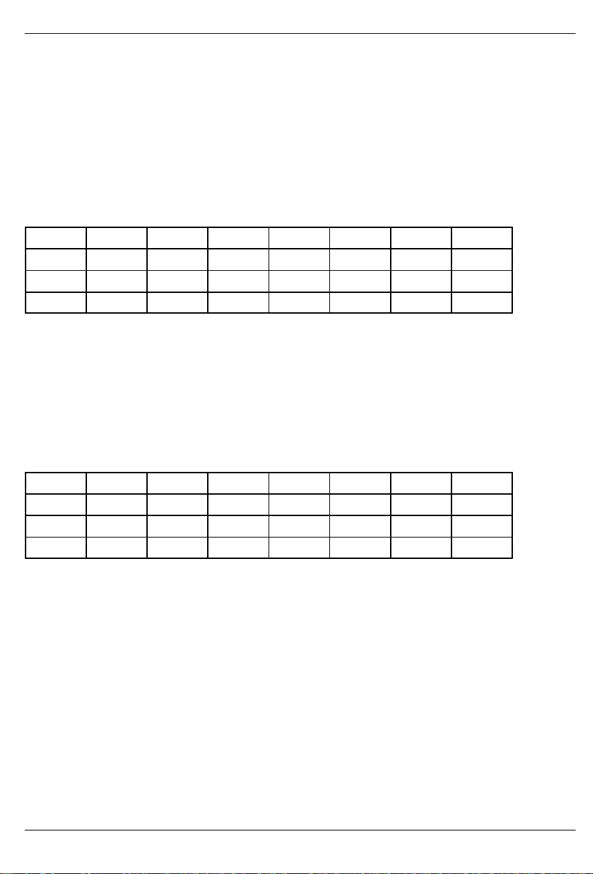
RECEIVE SIDE TIMING
FRAME#
RSYNC
RSYNC
RCLK
RLINK
1
2
3
4
15 16 1 2 3 4 5 6 7 8 9 10 11 12 13 14 15
1612345614
NOTES:
1. RSYNC in the frame mode (RCR1.6=0).
2. RSYNC in the multiframe mode (RCR1.6=1).
3. RLCLK is programmed to output just the Sa4 bit.
4. RLINK will always output all five Sa bits as well as the rest of the receive data stream.
5. This diagram assumes the CAS MF begins with the FAS word.
031397 24/40
Page 25

DS2143/DS2143Q
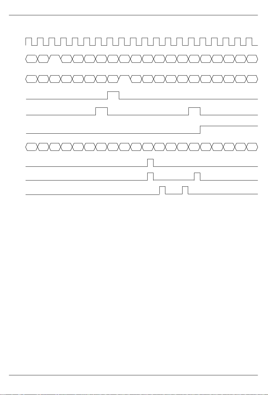
RECEIVE SIDE 1.544 MHZ BOUNDARY TIMING (WITH ELASTIC STORE ENABLED)
SYSCLK
1
RSER
RSYNC
RSYNC
RCHCLK
RCHBLK
LSB MSB LSB MSBF
2
3
4
CHANNEL 24/32 CHANNEL 1/2CHANNEL 23/31
NOTES:
1. Data from the E1 channels 1, 5, 9, 13, 17, 21, 25, and 29 is dropped (channel 2 from the E1 link is mapped to
channel 1 of the T1 link, etc.) and the F–bit position is added (forced to one).
2. RSYNC is in the output mode (RCR1.5=0).
3. RSYNC is in the input mode (RCR1.5=1).
4. RCHBLK is programmed to block channel 24.
RECEIVE SIDE 2.048 MHZ BOUNDARY TIMING (WITH ELASTIC STORE ENABLED)
SYSCLK
RSER
RSYNC
RSYNC
RCHCLK
RCHBLK
LSB MSB LSB MSB
1
2
3
CHANNEL 32 CHANNEL 1CHANNEL 31
NOTES:
1. RSYNC is in the output mode (RCR1.5=0).
2. RSYNC is in the input mode (RCR1.5=1).
3. RCHBLK is programmed to block channel 1.
031397 25/40
Page 26
DS2143/DS2143Q
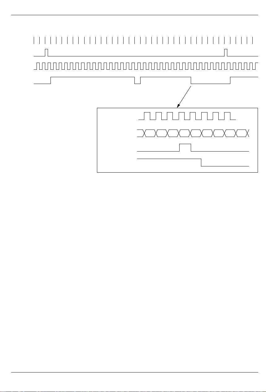
RECEIVE SIDE BOUNDARY TIMING (WITH ELASTIC STORE DISABLED)
RCLK
RPOS,
RNEG
LSB Si MSB LSB MSB
1
1 Sa4 Sa5 Sa6 Sa7 Sa8
CHANNEL 1 CHANNEL 2
A
1
RSER
RSYNC
RCHCLK
RCHBLK
RLINK
RLCLK
RLCLK
RLCLK
2
3
4
5
CHANNEL 32 CHANNEL 1 CHANNEL 2
Si 1 A Sa4 Sa5 Sa6 Sa7 Sa8
LSB MSB
NOTES:
1. There is a 6 RCLK delay from RPOS, RNEG to RSER.
2. RCHBLK is programmed to block channel 2.
3. RLINK is programmed to output the Sa4 bits.
4. RLINK is programmed to output the Sa4 and Sa8 bits.
5. RLINK is programmed to output the Sa5 and Sa7 bits.
6. Shown is a non–align frame boundary.
Sa4 Sa5 Sa6 Sa7 Sa8
031397 26/40
Page 27
DS2143/DS2143Q
G.802 TIMING
TIMESLOT# 30 31 0 1 2 3 4 5 6 7 8 9 10 11 12 13 14 15 16 17 18 19 20 21 22 23 24 25 26 27 28 29 30 31 0 1 2 3 4
RSYNC/
TSYNC
RCHCLK/
TCHCLK
RCHBLK/
1
TCHBLK
DETAIL
RCLK/TCLK
TIMESLOT 25 TIMESLOT 26
RSER/TSER
RCHCLK/TCHCLK
RCHBLK/TCHCLK
LSB MSB
NOTE:
1. RCHBLK/TCHBLK is programmed to pulse high during timeslots 1 to 15, 17 to 25, during bit 1 of timeslot 26.
031397 27/40
Page 28

DS2143/DS2143Q
TRANSMIT SIDE BOUNDARY TIMING
TCLK
1
TSER
LSB Si 1 A Sa4 Sa5 Sa6 Sa7 Sa8 MSB MSBLSB
CHANNEL 2CHANNEL 1
TPOS,
1
TNEG
TSYNC
TSYNC
MSB LSB Si 1 A Sa4 Sa5 Sa6 Sa7 Sa8 MSB
2
3
TCHCLK
4
TCHBLK
5
TLCLK
TLINK
TLCLK
TLINK
5
6
6
Don’t Care
Don’t Care
NOTES:
1. There is a 5 TCLK delay from TSER to TPOS, and TNEG.
2. TSYNC is in the input mode (TCR1.0=0).
3. TSYNC is in the output mode (TCR1.0=1).
4. TCHBLK is programmed to block channel 2.
5. TLINK is programmed to source the Sa4 bits.
6. TLINK is programmed to source the Sa7 and Sa8 bits.
7. Shown is a non–align frame boundary.
CHANNEL 2CHANNEL 1CHANNEL 32
Don’t CareDon’t Care
031397 28/40
Page 29
TRANSMIT SIDE TIMING
DS2143/DS2143Q
FRAME#
TSYNC
TSYNC
3
TCLK
TLINK
1
2
3
15 16 1 2 3 4 5 6 7 8 9 10 11 12 13 14 15
1612345614
NOTES:
1. TSYNC in the frame mode (TCR1.1=0).
2. TSYNC in the multiframe mode (TCR1.1=1).
3. TLINK is programmed to source only the Sa4 bit.
4. This diagram assumbes both the CAS MF and the CRC4 begin with the align frame.
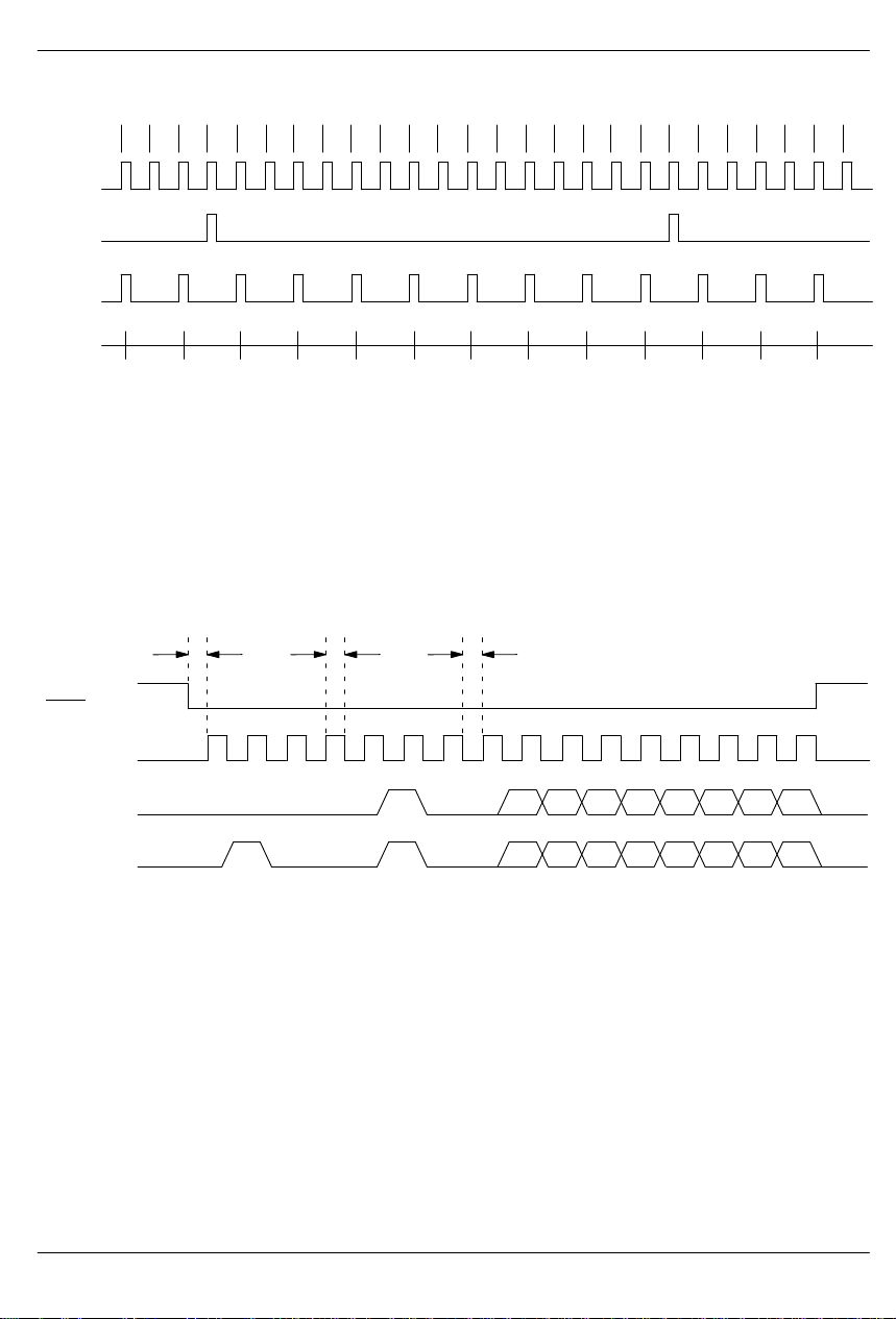
LINE INTERFACE CONTROL TIMING
244 ns 244 ns244 ns
LI_CS
LI_SCLK
1
LI_SDI
LI_SDI
2
00 0 0 0 0 0
000 00110
1
CR0 CR1 CR2 CR3 CR4 CR5 CR6 CR7
CR0 CR1 CR2 CR3 CR4 CR5 CR6 CR7
NOTES:
1. A write to CRB1 will cause the DS2143 to output this sequence.
2. A write to CRB2 will cause the DS2143 to output this sequence.
3. Timing numbers are based on RCLK=2.048 MHz with 50% duty cycle.
031397 29/40
Page 30
DS2143/DS2143Q
DS2143 SYNCHRONIZATION FLOWCHART
RLOS=1
RESYNC IF
RCR1.1=0
POWER UP
RLOS=1
FAS SYNC
CRITERIA MET
FASSA=0
INCREMENT CRC4
SYNC COUNTER;
CRC4SA=0
SET FASRC
(RIR.1)
CRC4 RESYNC
CRITERIA MET
CAS RESYNC
CRITERIA MET;
SET CASRC
(RIR.0)
8 MS
TIME
OUT
FAS RESYNC
CRITERIA MET
CHECK FOR >=915
OUT OF 1000 CRC
WORD ERRORS
CHECK FOR CAS
MF WORD ERROR
CRC4 MULTIFRAME
SEARCH (IF ENABLED
VIA CCR.0)
CRC4SA=1
CRC4 SYNC CRITERIA
MET; CRC4SA=0;
RESET CRC4 SYNC
COUNTER
CHECK FOR FAS
FRAMING ERROR
(DEPENDS ON
RCR1.2)
IF CRC4 IS ON
(CCR.0=1)
IF CAS IS ON
(CCR.3=0)
SYNC DECLARED
RLOS=0
CAS MULTIFRAME
SEARCH (IF ENABLED
VIA CCR.3)
CASSA=1
CAS SYNC
CRITERIA MET
CASSA=0
031397 30/40
Page 31
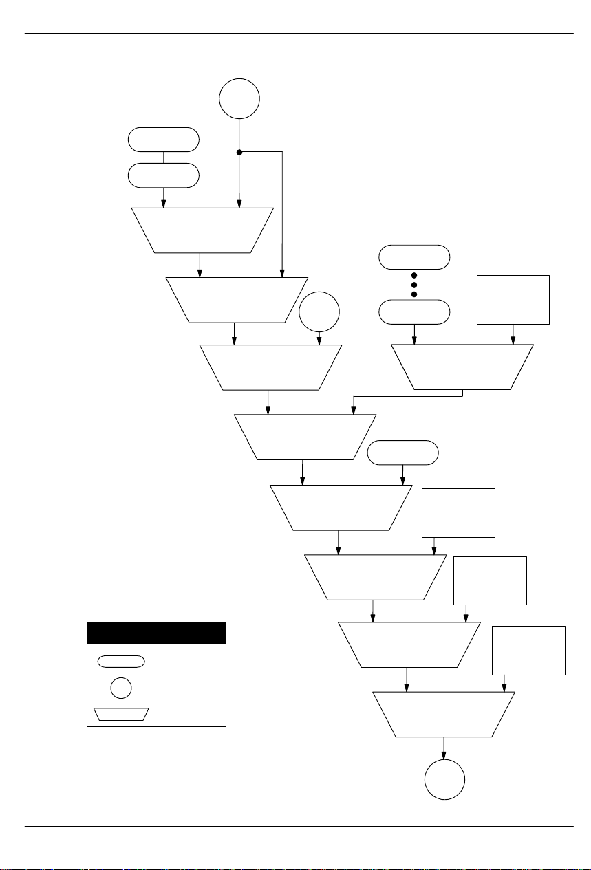
DS2143 TRANSMIT DATA FLOW
TAF
TNAF
DS2143/DS2143Q
TSER
0
TIMESLOT 0
PASS–THROUGH
(TCR1.6)
1
Si BIT INSERTION
CONTROL
(TCR1.3)
1
0
TLINK
00
Sa BIT INSERTION
CONTROL (TCR2.3
THRU TCR2.7)
TIMESLOT 16 SIGNALING
INSERTION CONTROL
11
0
(TCR1.5)
IDLE CODE INSERTION
1
0
CONTROL
(TIR1 TO TIR4)
0
E–BIT GENERATION
(TCR2.1)
TS0
TS15
TRANSMIT SIGNALLING
ALL ONES
(TCR1.2)
TIDR
1
RECEIVE SIDE
CRC4 ERROR
DETECTOR
1
AIS
GENERATION
CRC4 MF AND
CODE WORD
GENERATION
KEY
= REGISTER
= DEVICE PIN
= SELECTOR
0
CRC4 ENABLE
(CCR.4)
01
TRANSMIT UNFRAMED
1
ALL ONES
(TCR1.4)
TPOS,
TNEG
AIS
GENERATION
031397 31/40
Page 32
DS2143/DS2143Q
ABSOLUTE MAXIMUM RATINGS*
Voltage on Any Pin Relative to Ground –1.0V to +7.0V
Operating Temperature 0°C to 70°C
Storage Temperature –55°C to +125°C
Soldering Temperature 260°C for 10 seconds
* This is a stress rating only and functional operation of the device at these or any other conditions above those
indicated in the operation sections of this specification is not implied. Exposure to absolute maximum rating
conditions for extended periods of time may affect reliability.
RECOMMENDED DC OPERATION CONDITIONS (0°C to 70°C)
PARAMETER SYMBOL MIN TYP MAX UNITS NOTES
Logic 1 V
Logic 0 V
Supply V
IH
DD
2.0 V
IL
–0.3 +0.8 V
4.5 5.5 V
+0.3 V
DD
CAPACITANCE
PARAMETER SYMBOL MIN TYP MAX UNITS NOTES
Input Capacitance C
Output Capacitance C
IN
OUT
5 pF
7 pF
DC CHARACTERISTICS (0°C to 70°C; V
= 5V + 10%)
DD
PARAMETER SYMBOL MIN TYP MAX UNITS NOTES
Supply Current I
Input Leakage I
Output Leakage I
Output Current (2.4V) I
Output Current (0.4V) I
DD
LO
OH
OL
IL
–1.0 +1.0 µA 2
–1.0 mA
+4.0 mA
10 mA 1
1.0 µA 3
NOTES:
1. RCLK = TCLK = 2.048 MHz; VDD = 5.5V.
2. 0.0V < V
3. Applies to INT1
< VDD.
IN
and INT2 when 3-stated.
031397 32/40
Page 33

DS2143/DS2143Q
AC CHARACTERISTICS – PARALLEL PORT (0°C to 70°C; V
= 5V + 10%)
DD
PARAMETER SYMBOL MIN TYP MAX UNITS NOTES
Cycle Time t
CYC
Pulse Width, DS Low or RD High PW
Pulse Width, DS High or RD Low PW
Input Rise/Fall Times tR, t
R/W Hold Time t
R/W Setup Time Before DS High t
CS Setup Time Before DS, WR or
active
RD
RWH
RWS
t
CS Hold Time t
Read Data Hold Time t
Write Data Hold Time t
Muxed Address Valid to AS or
ALE fall
Muxed Address Hold Time t
Delay Time DS, WR or RD to AS
or ALE Rise
DHR
DHW
t
ASL
AHL
t
ASD
Pulse Width AS or ALE High PW
Delay Time, AS or ALE to DS,
or RD
WR
Output Data Delay Time from DS
or RD
Data Setup Time t
t
ASED
t
DDR
DSW
EL
EH
F
CS
CH
ASH
250 ns
150 ns
100 ns
30 ns
10 ns
50 ns
20 ns
0 ns
10 50 ns
0 ns
20 ns
10 ns
25 ns
40 ns
20 ns
20 100 ns
80 ns
031397 33/40
Page 34
DS2143/DS2143Q
INTEL WRITE AC TIMING
ALE
t
ASD
PW
ASH
t
CYC
RD
WR
CS
AD0-AD7
INTEL READ AC TIMING
ALE
t
ASD
WR
RD
PW
t
t
ASD
ASD
t
ASED
PW
PW
EH
t
CH
t
DHW
t
DSW
EH
t
CH
PW
EL
t
CS
t
ASL
t
AHL
t
CYC
PW
ASH
t
ASED
EL
t
CS
CS
AD0-AD7
031397 34/40
t
ASL
t
AHL
t
DDR
t
DHR
Page 35
MOTOROLA AC TIMING
AS
DS
R/W
t
ASD
PW
PW
EL
ASH
t
t
RWS
ASED
t
CYC
PW
DS2143/DS2143Q
EH
t
RWH
AD0-AD7
(READ)
CS
AD0-AD7
(WRITE)
t
ASL
t
ASL
t
t
AHL
AHL
t
DDR
t
CS
t
DSW
t
DHR
t
CH
t
DHW
031397 35/40
Page 36

DS2143/DS2143Q
AC CHARACTERISTICS – TRANSMIT SIDE (0°C to 70°C; VDD = 5V + 10%)
PARAMETER SYMBOL MIN TYP MAX UNITS NOTES
TCLK Period t
TCLK Pulse Width t
CH
t
TSER, TSYNC, TLINK Setup to
TCLK Falling
TSER, TLINK Hold from TCLK
Falling
t
SU
t
HD
TCLK Rise/Fall Times tR, t
Data Delay t
TSYNC Pulse Width t
DD
PW
CL
P
50
50
25 ns
25 ns
F
50 ns
488 ns
ns
ns
25 ns
50 ns
AC CHARACTERISTICS – RECEIVE SIDE (0°C to 70°C; VDD = 5V ± 10%)
PARAMETER SYMBOL MIN TYP MAX UNITS NOTES
RCLK and SYSCLK Period t
RCLK and SYSCLK Pulse Width t
CH
t
RPOS, RNEG, RSYNC, Setup to
RCLK Falling
RPOS, RNEG, Hold from RCLK
Falling
t
SU
t
HD
RCLK Rise/Fall Times tR, t
Data Delay t
RSYNC Pulse Width t
DD
PW
CL
P
50
50
25 ns
25 ns
F
50 ns
488 ns
ns
ns
25 ns
60 ns
031397 36/40
Page 37

DS2143/DS2143Q
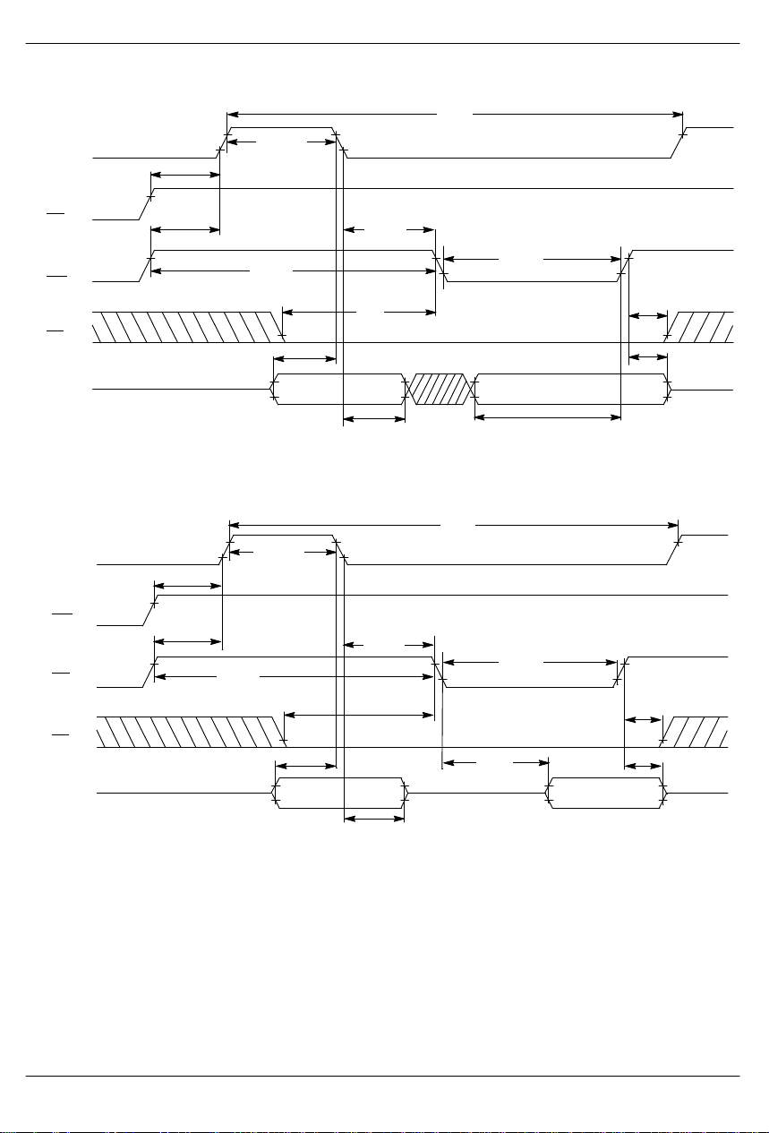
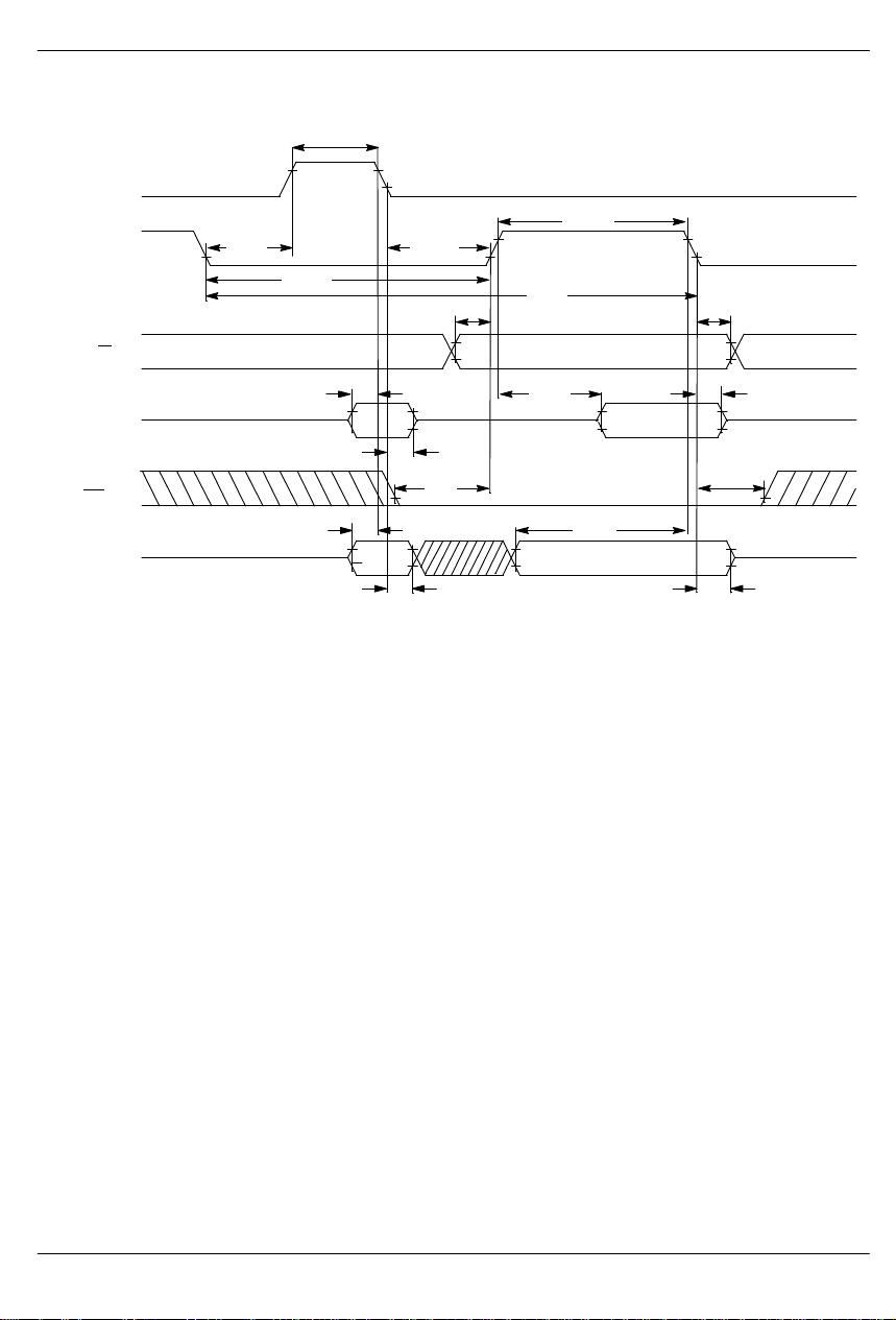
TRANSMIT SIDE AC TIMING
t
R
TCLK
t
DD
TPOS,
TNEG
TSER
TCHCLK
TCHBLK
1
TSYNC
2
TSYNC
t
P
t
t
F
t
t
DD
t
DD
t
DD
t
SU
t
DD
HD
t
SU
t
PW
CL
t
CH
3
TLCLK
t
HD
TLINK
t
3
SU
NOTES:
1. TSYNC is in the output mode (TCR1.0=1).
2. TSYNC is in the input mode (TCR1.0=0).
3. No timing relationship between TSYNC and TLCLK/TLINK is implied.
031397 37/40
Page 38

DS2143/DS2143Q
RECEIVE SIDE AC TIMING
t
R
SYSCLK
RCLK
RSER
RPOS,
RNEG
RCHCLK
RCHBLK
1
RSYNC
2
RSYNC
t
P
t
t
F
t
DD
t
t
DD
t
DD
t
DD
t
SU
HD
t
SU
t
PW
CL
t
CH
t
DD
3
RLCLK
t
DD
3
RLINK
NOTES:
1. RSYNC is in the output mode (RCR1.5=0).
2. RSYNC is in the input mode (RCR1.5=1).
3. No timing relationship between RSYNC and RLCLK/RLINK is implied.
031397 38/40
Page 39
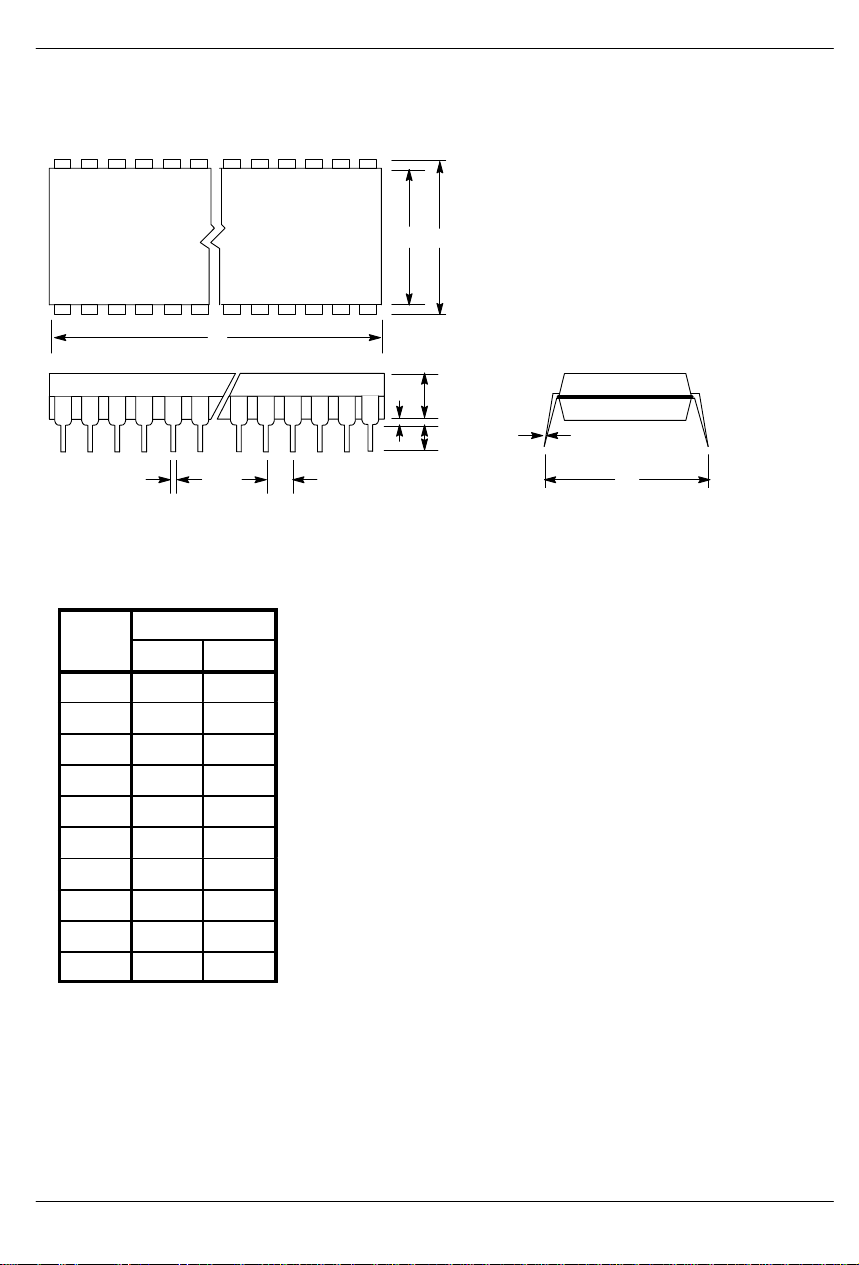
DS2143 E1 CONTROLLER (600 MIL) 40–PIN DIP
40
B
DS2143/DS2143Q
D
1
KG H
INCHES
DIM MIN MAX
A 2.040 2.070
B 0.530 0.560
C 0.145 0.155
D 0.600 0.625
E 0.015 0.040
F 0.120 0.140
G 0.090 0.110
H 0.625 0.675
J 0.008 0.012
K 0.015 0.022
A
E
C
F
J
031397 39/40
Page 40
DS2143/DS2143Q
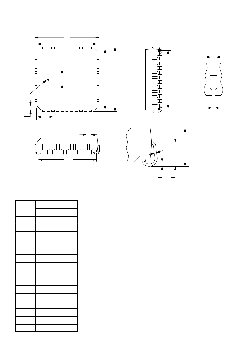
DS2143 E1 CONTROLLER 44–PIN PLCC
E
E1
B
N
1
.075 MAX
D1
D
NOTE 1
CH1
.150
MAX
e1
E2
NOTE1: PIN 1 IDENTIFIER TO BE LOCA TED IN ZONE INDICATED.
INCHES
DIM MIN MAX
A 0.165 0.180
A1 0.090 0.120
A2 0.020 –
B 0.026 0.033
B1 0.013 0.021
C 0.009 0.012
CH1 0.042 0.048
D 0.685 0.695
D1 0.650 0.656
D2 0.590 0.630
E 0.685 0.695
E1 0.650 0.656
E2 0.590 0.630
e1 0.050 BSC
N 44 –
D2
B1
A
C
A1A2
031397 40/40
 Loading...