

Page 1
DS2141A
DS2141A
T1 Controller
FEATURES
• DS1/ISDN–PRI framing transceiver
• Frames to D4, ESF, and SLC–96 formats
• Parallel control port
• Onboard, dual two–frame elastic store slip buffers
• Extracts and inserts robbed–bit signaling
• Programmable output clocks
• Onboard FDL support circuitry
• 5V supply; low–power CMOS
• Available in 40–pin DIP and 44–pin PLCC (DS2141Q)
• Compatible with DS2186 Transmit Line Interface,
DS2187 Receive Line Interface, DS2188 Jitter Attenuator, DS2290 T1 Isolation Stik, and DS2291 T1 Long
Loop Stik.
DESCRIPTION
The DS2141A is a comprehensive, software–driven T1
framer. It is meant to act as a slave or coprocessor to a
microcontroller or microprocessor. Quick access via
the parallel control port allows a single micro to handle
many T1 lines. The DS2141A is very flexible and can be
configured into numerous orientations via software.
The software orientation of the device allows the user to
modify their design to conform to future T1 specification
changes. The controller contains a set of 62 8–bit internal registers which the user can access. These internal
registers are used to configure the device and obtain information from the T1 link. The device fully meets all of
the latest T1 specifications including ANSI
T1.403–1989, AT&T TR 62411 (12–90), and CCITT
G.704 and G.706.
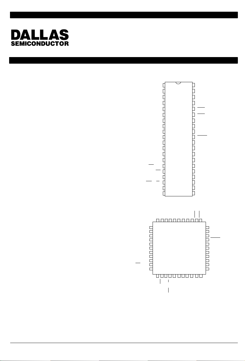
PIN ASSIGNMENT
1
TCLK
2
TSER
AD0
AD1
AD2
AD3
AD4
AD5
AD6
AD7
BTS
RD (DS)
NC
TCHCLK
RD
ALE(AS)
WR
3
TPOS
4
5
TNEG
6
AD0
7
AD1
8
AD2
9
AD3
10
AD4
11
AD5
12
AD6
13
AD7
14
BTS
15
(DS)
16
CS
17
18
(R/W)
19
RLINK
20 21
VSS
40–PIN DIP (600 MIL)
TNEG
TPOS
TCHCLK
7
8
9
10
11
12
44–PIN PLCC
13
14
15
16
17
1819 202122 2324
CS
NC
ALE(AS)
TSER
TCLK
VDD
123456 44 43 42 41 40
VSS
RLINK
WR(R/W)
40
39
38
37
36
35
34
33
32
31
30
29
28
27
26
25
24
23
22
TSYNC
TLINK
TLCLK
25 262728
RCLK
RLCLK
RCHCLK
VDD
TSYNC
TLINK
TLCLK
INT1
INT2
RLOS/LOTC
TCHBLK
RCHBLK
LI_CS
LI_CLK
LI_SDI
SYSCLK
RNEG
RPOS
RSYNC
RSER
RCHCLK
RCLK
RLCLK
INT1
INT2
RLOS/LOTC
39
TCHBLK
38
RCHBLK
37
LI_CS
36
LI_CLK
35
LI_SDI
34
NC
33
NC
32
SYSCLK
31
RNEG
30
RPOS
29
RSER
RSYNC
Copyright 1995 by Dallas Semiconductor Corporation.
All Rights Reserved. For important information regarding
patents and other intellectual property rights, please refer to
Dallas Semiconductor data books.
021997 1/35
Page 2
DS2141A
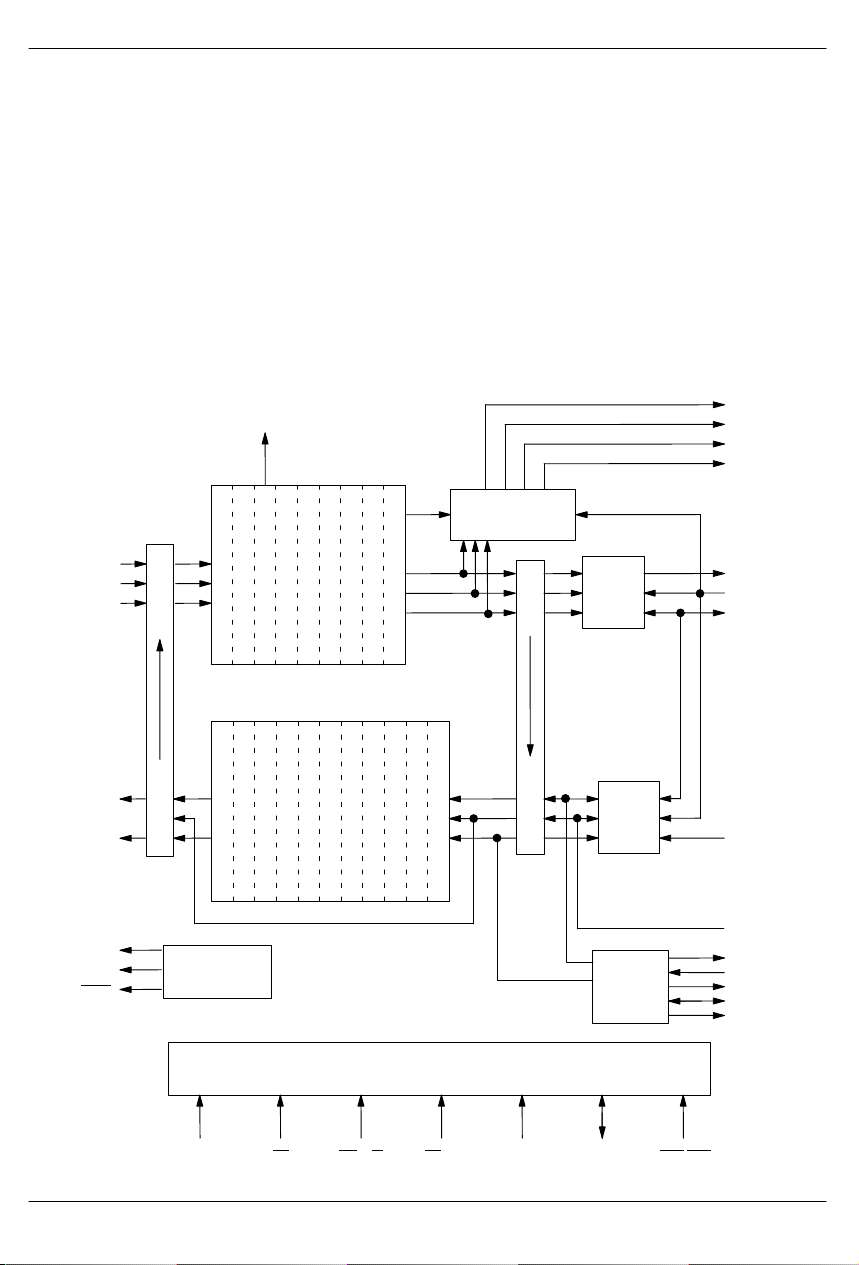
1.0 INTRODUCTION
The DS2141A T1 Controller has four main sections: the
receive side, the transmit side, the line interface controller, and the parallel control port. See the block diagram
below. On the receive side, the device will clock in the
serial T1 stream via the RPOS and RNEG pins. The
synchronizer will locate the frame and multiframe patterns and establish their respective positions. This information will be used by the rest of the receive side circuitry.
The DS2141A is an “off–line” framer , which means that
all of the T1 serial stream that goes into the device will
DS2141A BLOCK DIAGRAM
RLOS
RECEIVE SIDE
FRAMER
RPOS
RCLK
RNEG
BPV COUNTER
B8ZS DECODER
SYNCHRONIZER
ALARM DETECTION
LOOP CODE DETECTOR
SIGNALING EXTRACTION
ONE’S DENSITY MONITOR
CRC/FRAME ERROR COUNT
come out of it unchanged. Once the T1 data has been
framed to, the robbed–bit signaling data and FDL can be
extracted. The 2–frame elastic stores can either be enabled or bypassed.
The transmit side clocks in the unframed T1 stream at
TSER and adds in the framing pattern, the robbed–bit
signaling, and the FDL. The line interface control port
will update line interface devices that contain a serial
port. The parallel control port contains a multiplexed address and data structure which can be connected to either a microcontroller or microprocessor.
TIMING CONTROL/
FDL EXTRACTION
ELASTIC
STORE
CHANNEL MARKING
RLINK
RLCLK
RCHBLK
RCHCLK
RSER
SYSCLK
RSYNC
TPOS
TNEG
LI_SDI
LI_SCLK
LI_CS
021997 2/35
TRANSMIT SIDE FORMATTER
LOCAL LOOPBACK
PAYLOAD LOOPBACK
AIS GEN.
B8ZS ENCODE
LINE INTERFACE
CONTROL PORT
BTS CS WR(R/W)RD(DS) ALE(AS) INT1/INT2AD0–AD7
YELLOW ALARM GEN.
CRC GEN.
FDL INSERTION
F–BIT INSERTION
LOOP CODE GEN.
ONE’S DENSITY ENCODER
PARALLEL CONTROL PORT
(ROUTED TO ALL BLOCKS)
CLEAR CHANNEL
IDLE CODE INSERTION
SIGNALING INSERTION
ELASTIC
STORE
TIMING
CONTROL/
FDL
INSERT
TSER
TCLK
TCHBLK
TLINK
TLCLK
TSYNC
TCHCLK
Page 3

DS2141A
DS2141A FEATURES
• parallel control port
• large error counters
• onboard dual 2–frame elastic store
• FDL support circuitry
• robbed–bit signaling extraction and insertion
• programmable output clocks
• fully independent transmit and receive sections
• error–tolerant yellow and blue alarm detection
• output pin test mode
• payload loopback capability
• SLC–96 support
• remote loop up/down code detection
• loss of transmit clock detection
• loss of receive clock detection
• 1’s density violation detection
• frame sync generation
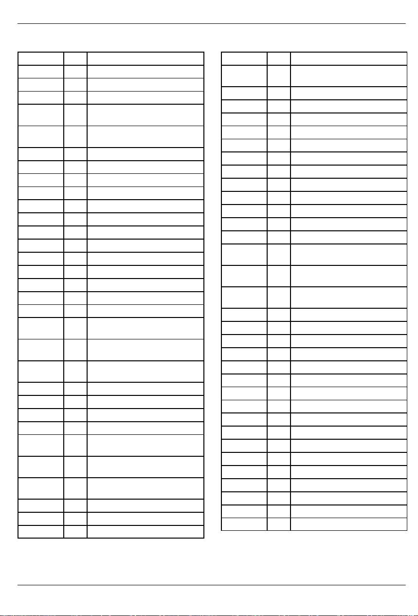
PIN DESCRIPTION Table 1
PIN SYMBOL TYPE DESCRIPTION
1 TCLK I Transmit Clock. 1.544 MHz primary clock.
2 TSER I Transmit Serial Data. Transmit NRZ serial data, sampled on the
3 TCHCLK O Transmit Channel Clock. 192 KHz clock which pulses high during
4
5
6–13 AD0–AD7 I/O Address/Data Bus. An 8–bit multiplexed address/data bus.
14 BTS I Bus Type Select. Strap high to select Motorola bus timing; strap low
15 RD(DS) I Read Input (Data Strobe).
16 CS I Chip Select. Must be low to read or write the port.
17 ALE(AS) I Address Latch Enable (Address Strobe). A positive–going edge
18 WR(R/W) I Write Input (Read/Write).
19 RLINK O Receive Link Data. Updated with either FDL data (ESF) or Fs–bits
20 VSS – Signal Ground. 0.0 volts.
21 RLCLK O Receive Link Clock. 4 KHz or 2 KHz (ZBTSI) demand clock for the
22 RCLK I Receive Clock. 1.544 MHz primary clock.
23 RCHCLK O Receive Channel Clock. 192 KHz clock which pulses high during
24 RSER O Receive Serial Data. Received NRZ serial data; updated on rising
TPOS
TNEG
falling edge of TCLK.
the LSB of each channel. Useful for parallel–to–serial conversion of
channel data, locating robbed–bit signaling bits, and for blocking
clocks in DDS applications. See Section 13 for timing details.
O Transmit Bipolar Data. Updated on rising edge of TCLK.
to select Intel bus timing. This pin controls the function of the
(DS), ALE(AS), and WR(R/W) pins. If BTS=1, then these pins
RD
assume the function listed in parenthesis ().
serves to demultiplex the bus.
(D4) or Z–bits (ZBTSI) one RCLK before the start of a frame. See
Section 13 for timing details.
RLINK input. See Section 13 for timing details.
the LSB of each channel. Useful for parallel–to–serial conversion of
channel data, locating robbed–bit signaling bits, and for blocking
clocks in DDS applications. See Section 13 for timing details.
edges of RCLK.
021997 3/35
Page 4

DS2141A
PIN DESCRIPTIONTYPESYMBOL
25 RSYNC I/O Receive Sync. An extracted pulse, one RCLK wide, is output at this
pin which identifies either frame (RCR2.4=0) or multiframe boundaries (RCR2.4=1). If set to output frame boundaries, then via
RCR2.5, RSYNC can also be set to output double–wide pulses on
signaling frames. If the elastic store is enabled via the CCR1.2, then
this pin can be enabled to be an input via RCR2.3 at which a frame
boundary pulse is applied. See Section 13 for timing details.
26
27
RPOS
RNEG
I Receive Bipolar Data Inputs. Sampled on falling edge of RCLK. Tie
together to receive NRZ data and disable bipolar violation monitoring
circuitry.
28 SYSCLK I System Clock. 1.544 MHz or 2.048 MHz clock. Only used when the
elastic store function is enabled via the CCR. Should be tied low in
applications that do not use the elastic store.
29 LI_SDI O Serial Port Data for the Line Interface. Connects directly to the SDI
input pin on the line interface.
30 LI_CLK O Serial Port Clock for the Line Interface. Connects directly to the
SCLK input pin on the line interface.
31 LI_CS O Serial Port Chip Select for the Line Interface. Connects directly to
input pin on the line interface.
the CS
32
33
RCHBLK
TCHBLK
O Receive/Transmit Channel Block. A user–programmable output
that can be forced high or low during any of the 24 T1 channels.
Useful for blocking clocks to a serial UART or LAPD controller in
application where not all T1 channels are used such as Fractional
T1, 384K bps service, 768K bps, or ISDN–PRI. Also useful for locating individual channels in drop–and–insert applications. See Section
13 for timing details.
34 RLOS/LOTC O Receive Loss of Sync/Loss of Transmit Clock. A dual function
output. If CCR1.6=0, then this pin will toggle high when the synchronizer is searching for the T1 frame and multiframe. If CCR1.6=1,
then this pin will toggle high when the TCLK pin has not been toggled
for 5 µs.
35 INT2 O Receive Alarm Interrupt 2. Flags host controller during conditions
defined in Status Register 2. Active low, open drain output.
36 INT1 O Receive Alarm Interrupt 1. Flags host controller during alarm condi-
tions defined in Status Register 1. Active low, open drain output.
37 TLCLK O Transmit Link Clock. 4 KHz or 2 KHz (ZBTSI) demand clock for the
TLINK input. See Section 13 for timing details.
38 TLINK I Transmit Link Data. If enabled via TCR1.2, this pin will be sampled
during the F–bit time on the falling edge of TCLK for data insertion
into either the FDL stream (ESF) or the Fs–bit position (D4) or the
Z–bit position (ZBTSI). See Section 13 for timing details.
39 TSYNC I/O Transmit Sync. A pulse at this pin will establish either frame or mul-
tiframe boundaries for the DS2141A. Via TCR2.2, the DS2141A can
be programmed to output either a frame or multiframe pulse at this
pin. If this pin is set to output pulses at frame boundaries, it can also
be set via TCR2.4 to output double–wide pulses at signaling frames.
See Section 13 for timing details.
40 VDD – Positive Supply. 5.0 volts.
021997 4/35
Page 5
DS2141A REGISTER MAP
ADDRESS R/W REGISTER NAME
20 R/W Status Register 1
21 R/W Status Register 2
22 R/W Receive Information Register
23 R Bipolar Violation/ESF Error
Event Count Register 1
24 R Bipolar Violation/ESF Error
Event Count Register 2
25 R CRC6 Count Register 1
26 R CRC6 Count Register 2.
27 R Frame Error Count Register
28 R Receive FDL Register
29 R/W Receive FDL Match Register 1
2A R/W Receive FDL Match Register 2
2B R/W Receive Control Register 1
2C R/W Receive Control Register 2
2D R/W Receive Mark Register 1
2E R/W Receive Mark Register 2
2F R/W Receive Mark Register 3
30 Not Assigned
31 Not Assigned
32 R/W Transmit Channel Blocking
Register 1
33 R/W Transmit Channel Blocking
Register 2
34 R/W Transmit Channel Blocking
Register 3
35 R/W Transmit Control Register 1
36 R/W Transmit Control Register 2
37 R/W Common Control Register 1
38 R/W Common Control Register 2
39 R/W Transmit Transparency
Register 1
3A R/W Transmit Transparency
Register 2
3B R/W Transmit Transparency
Register 3
3C R/W Transmit Idle Register 1
3D R/W Transmit Idle Register 2
3E R/W Transmit Idle Register 3
DS2141A
ADDRESS R/W REGISTER NAME
3F R/W Transmit Idle Definition
Register
60 R Receive Signaling Register 1
61 R Receive Signaling Register 2
62 R Receive Signaling Register 3
63 R Receive Signaling Register 4
64 R Receive Signaling Register 5
65 R Receive Signaling Register 6
66 R Receive Signaling Register 7
67 R Receive Signaling Register 8
68 R Receive Signaling Register 9
69 R Receive Signaling Register 10
6A R Receive Signaling Register 11
6B R Receive Signaling Register 12
6C R/W Receive Channel Blocking
Register 1.
6D R/W Receive Channel Blocking
Register 2
6E R/W Receive Channel Blocking
Register 3
6F R/W Interrupt Mask Register 2
70 R/W Transmit Signaling Register 1
71 R/W Transmit Signaling Register 2
72 R/W Transmit Signaling Register 3
73 R/W Transmit Signaling Register 4
74 R/W Transmit Signaling Register 5
75 R/W Transmit Signaling Register 6
76 R/W Transmit Signaling Register 7
77 R/W Transmit Signaling Register 8
78 R/W Transmit Signaling Register 9
79 R/W Transmit Signaling Register 10
7A R/W Transmit Signaling Register 11
7B R/W Transmit Signaling Register 12
7C R/W LI Control Register Byte 1
7D R/W LI Control Register Byte 2
7E R/W Transmit FDL Register
7F R/W Interrupt Mask Register 1
Note: All values indicated within the Address column
are hexadecimal.
021997 5/35
Page 6

DS2141A
2.0 P ARALLEL PORT
The DS2141A is controlled via a multiplexed bidirectional
address/data bus by an external microcontroller or microprocessor. The DS2141A can operate with either Intel or
Motorola bus timing configurations. If the BTS pin is tied
pulses. In a read cycle, the DS2141A outputs a byte of
data during the latter portion of the DS or RD
read cycle is terminated and the bus returns to a high impedance state as RD transitions high in Intel timing or as
DS transitions low in Motorola timing.
low, Intel timing will be selected; if tied high, Motorola timing will be selected. All Motorola bus signals are listed in
parenthesis (). See the timing diagrams in the AC Electrical Characteristics for more details. The multiplexed bus
on the DS2141A saves pins bec ause the address information and data information share the same signal
paths. The addresses are presented to the pins in the
first portion of the bus cycle and data will be transferred
on the pins during second portion of the bus cycle. Addresses must be valid prior to the falling edge of ALE(AS),
at which time the DS2141A latches the address from the
AD0 to AD7 pins. Valid write data must be present and
held stable during the later portion of the DS or WR
3.0 CONTROL REGISTERS
The operation of the DS2141A is configured via a set of
six registers. Typically , the control registers are only ac-
cessed when the system is first powered up. Once, the
DS2141A has been initialized, the control registers will
only need to be accessed when there is a change in the
system configuration. There are two Receive Control
Registers (RCR1 and RCR2), two Transmit Control
Registers (TCR1 and TCR2), and two Common Control
Registers (CCR1 and CCR2). Each of the six registers
is described below.
RCR1: RECEIVE CONTROL REGISTER 1 (2Bh)
(MSB) (LSB)
– ARC OOF1 OOF2 SYNCC SYNCT SYNCE RESYNC
SYMBOL POSITION NAME AND DESCRIPTION
– RCR1.7 Not Assigned. Should be set to 0 when written to.
ARC RCR1.6 Auto Resync Criteria.
OOF1 RCR1.5 Out Of Frame Select 1.
OOF2 RCR1.4 Out Of Frame Select 2.
SYNCC RCR1.3 Sync Criteria.
SYNCT RCR1.2 Sync Time.
SYNCE RCR1.1 Sync Enable.
RESYNC RCR1.0 Resync. When toggled from low to high, a resync is initiated. Must be
0=Resync on OOF or RCL event.
1=Resync on OOF only.
0=2/4 frame bits in error.
1=2/5 frame bits in error.
0=follow RCR1.5.
1=2/6 frame bits in error.
In D4 Framing Mode.
0=search for Ft pattern, then search for Fs pattern.
1=cross couple Ft and Fs pattern.
In ESF Framing Mode.
0=search for FPS pattern only.
1=search for FPS and verify with CRC6.
0=qualify 10 bits.
1=qualify 24 bits.
0=auto resync enabled.
1=auto resync disabled.
cleared and set again for a subsequent resync.
pulses. The
021997 6/35
Page 7

RCR2: RECEIVE CONTROL REGISTER 2 (2Ch)
(MSB) (LSB)
RCS RZBTSI RSDW RSM RSIO RD4YM FSBE BPVCRS
SYMBOL POSITION NAME AND DESCRIPTION
RCS RCR2.7 Receive Code Select.
0=idle code (7F Hex).
1=digital milliwatt code (1E/0B/0B/1E/9E/8B/8B/9E Hex).
RZBTSI RCR2.6 Receive Side ZBTSI Enable.
0=ZBTSI disabled.
1=ZBTSI enabled.
RSDW RCR2.5 RSYNC Double–Wide.
0=do not pulse double–wide in signaling frames.
1=do pulse double–wide in signaling frames.
(note: this bit must be set to 0 when RCR2.4 = 1 or when RCR2.3 = 1).
RSM RCR2.4 RSYNC Mode Select.
0=frame mode (see the timing in Section 13).
1=multiframe mode (see the timing in Section 13).
RSIO RCR2.3 RSYNC I/O Select.
0=RSYNC is an output.
1=RSYNC is an input (only valid if elastic store enabled).
(note: this bit must be set to 0 when CCR1.2 = 0).
RD4YM RCR2.2 Receive Side D4 Yellow Alarm Select.
0=0 in bit 2 of all channels.
1=a 1 in the S–bit position of frame 12.
FSBE RCR2.1 Fs–Bit Error Report Enable.
0=do not report bit errors in the Fs–bit position in FECR.
1=report bit errors in the Fs–bit position in FECR.
BPVCRS RCR2.0 BPVCRS Function Select.
0=counts bipolar violations.
1=counts ESF error events (CRC6 OR ’ed with RLOS).
DS2141A
021997 7/35
Page 8

DS2141A
TCR1: TRANSMIT CONTROL REGISTER 1 (35h)
(MSB) (LSB)
ODF TFPT TCPT RBSE GB7S TLINK TBL TYEL
SYMBOL POSITION NAME AND DESCRIPTION
ODF TCR1.7 Output Data Format.
TFPT TCR1.6 Transmit Framing Pass Through.
TCPT TCR1.5 Transmit CRC Pass Through.
RBSE TCR1.4 Robbed Bit Signaling Enable.
GB7S TCR1.3 Global Bit 7 Stuffing.
TLINK TCR1.2 TLINK Select.
TBL TCR1.1 Transmit Blue Alarm.
TYEL TCR1.0 Transmit Yellow Alarm.
0=bipolar data at TPOS and TNEG.
1=NRZ data at TPOS; TNEG = 0.
0=Ft or FPS bits sourced internally.
1=Ft or FPS bits sampled at TSER during F–bit time.
0=source CRC6 bits internally.
1=CRC6 bits sampled at TSER during F–bit time.
0=no signaling is inserted in any channel.
1=signaling is inserted in all channels (the TTR registers can be used to
block insertion on a channel by channel basis).
0=allow the TTR registers to determine which channels containing all zeros
are to be bit 7 stuffed.
1=force bit 7 stuffing in all zero byte channels regardless of how the TTR
registers are programmed.
0=source FDL or Fs bits from TFDL register.
1=source FDL or Fs bits from the TLINK pin.
0=transmit data normally.
1=transmit an unframed all 1’s code at TPOS and TNEG.
0=do not transmit yellow alarm.
1=transmit yellow alarm.
TCR2: TRANSMIT CONTROL REGISTER 2 (36h)
(MSB) (LSB)
TESTM
SYMBOL POSITION NAME AND DESCRIPTION
TESTM TCR2.7 Test Mode Select. Set this bit to a 1 to force all outputs (including I/O pins)
TESTIO TCR2.6 Test I/O Pins.
TZBTSI TCR2.5 Transmit Side ZBTSI Enable.
021997 8/35
TESTIO TZBTSI TSDW TSM TSIO TD4YM B7ZS
either high (TCR2.6 = 1) or low (TCR2.6 = 0).
0=force all output (and I/O) pins to a logic 0.
1=force all output (and I/O) pins to a logic 1.
0=ZBTSI disabled.
1=ZBTSI enabled.
Page 9

DS2141A
TSDW TCR2.4 TSYNC Double–Wide.
0=do not pulse double–wide in signaling frames.
1=do pulse double–wide in signaling frames.
(note: this bit must be set to 0 when TCR2.3 = 1 or when TCR2.2 = 0).
TSM TCR2.3 TSYNC Mode Select.
0=frame mode (see the timing in Section 13).
1=multiframe mode (see the timing in Section 13).
TSIO TCR2.2 TSYNC I/O Select.
0=TSYNC is an input.
1=TSYNC is an output.
TD4YM TCR2.1 Transmit Side D4 Yellow Alarm Select.
0=0s in bit 2 of all channels.
1=a 1 in the S–bit position of frame 12.
B7ZS TCR2.0 Bit 7 Zero Suppression Enable.
0=no stuffing occurs.
1=Bit 7 forced to a 1 in channels with all 0s.
CCR1: COMMON CONTROL REGISTER 1 (37h)
(MSB) (LSB)
TESE P34F RSAO – SCLKM RESE PLB LLB
SYMBOL POSITION NAME AND DESCRIPTION
TESE CCR1.7 Transmit Elastic Store Enable.
P34F CCR1.6 Function of Pin 34.
RSAO CCR1.5 Receive Signaling All 1’s.
– CCR1.4 Not Assigned. Should be set to 0 when written to.
SCLKM CCR1.3 SYSCLK Mode Select.
RESE CCR1.2 Receive Elastic Store Enable.
PLB CCR1.1 Payload Loopback.
LLB CCR1.0 Local Loopback.
0=elastic store is bypassed.
1=elastic store is enabled.
0=Receive Loss of Sync (RLOS).
1=Loss of Transmit Clock (LOTC).
0=allow robbed signaling bits to appear at RSER.
1=force all robbed signaling bits at RSER to 1.
0=if SYSCLK is 1.544 MHz.
1=if SYSCLK is 2.048 MHz.
0=elastic store is bypassed.
1=elastic store is enabled.
0=loopback disabled.
1=loopback enabled.
0=loopback disabled.
1=loopback enabled.
021997 9/35
Page 10

DS2141A
PAYLOAD LOOPBACK
When CCR1.1 is set to a 1, the DS2141A will be forced
5. The TLCLK signal will become synchronous with
RCLK instead of TCLK.
into Payload LoopBack (PLB). Normally, this loopback
is only enabled when ESF framing is being performed.
In a PLB situation, the DS2141A will loop the 192 bits of
payload data (with BPVs corrected) from the receive
section back to the transmit section. The FPS framing
pattern, CRC6 calculation, and the FDL bits are not
looped back, they are reinserted by the DS2141A.
When PLB is enabled, the following will occur:
LOCAL LOOPBACK
When CCR1.0 is set to a 1, the DS2141A will enter a Local LoopBack (LLB) mode. This loopback is useful in
testing and debugging applications. In LLB, the
DS2141A will loop data from the transmit side back to
the receive side. This loopback is synonymous with replacing the RCLK input with the TCLK signal, and the
RPOS/RNEG inputs with the TPOS/TNEG outputs.
1. Data will be transmitted from the TPOS and TNEG
When LLB is enabled, the following will occur:
pins synchronous with RCLK instead of TCLK.
2. All of the receive side signals will continue to operate
normally .
3. The TCHCLK and TCHBLK signals are forced low.
4. Data at the TSER pin is ignored.
1. The TPOS and TNEG pins will transmit an unframed
all 1s.
2. Data at RPOS and RNEG will be ignored.
3. All receive side signals will take on timing synchronous with TCLK instead of RCLK.
CCR2: COMMON CONTROL REGISTER 2 (38h)
(MSB) (LSB)
TFM TB8ZS TSLC96 TFDL RFM RB8ZS RSLC96 RFDL
SYMBOL POSITION NAME AND DESCRIPTION
TFM CCR2.7 Transmit Frame Mode Select.
TB8ZS CCR2.6 Transmit B8ZS Enable.
TSLC96 CCR2.5 Transmit SLC–96/Fs Bit Insertion Enable.
TFDL CCR2.4 Transmit Zero Stuffer Enable.
RFM CCR2.3 Receive Frame Mode Select.
RB8ZS CCR2.2 Receive B8ZS Enable.
0=D4 framing mode.
1=ESF framing mode.
0=B8ZS disabled.
1=B8ZS enabled.
0=SLC–96 disabled.
1=SLC–96 enabled.
0=zero stuffer disabled.
1=zero stuffer enabled.
0=D4 framing mode.
1=ESF framing mode.
0=B8ZS disabled.
1=B8ZS enabled.
021997 10/35
Page 11

DS2141A
RSLC96 CCR2.1 Receive SLC–96 Enable.
0=SLC–96 disabled.
1=SLC–96 enabled.
RFDL CCR2.0 Receive Zero Destuffer Enable.
0=zero destuffer disabled.
1=zero destuffer enabled.
4.0 STATUS AND INFORMATION
REGISTERS
There is a set of three registers that contain information
on the current real time status of the DS2141A: Status
Register 1 (SR1), Status Register 2 (SR2), and the Receive Information Register (RIR). When a particular
event has occurred (or is occurring), the appropriate bit
in one of these three registers will be set to a 1. All of the
bits in these registers operate in a latched fashion. This
means that if an event occurs and a bit is set to a 1 in any
of the registers, it will remain set until the user reads that
bit. The bit will be cleared when it is read and it will not be
set again until the event has occurred again (or in the
case of RLOS, if loss of sync is still present).
The user will always precede a read of these registers
with a write. The byte written to the register will inform
the DS2141A which bits the user wishes to read and
have cleared. The user will write a byte to one of these
three registers, with a 1 in the bit positions he or she
wishes to read and a 0 in the bit positions he or she does
not wish to obtain the latest information on. When a 1 is
written to a bit location, the read register will be updated
with current value and it will be cleared. When a 0 is written to a bit position, the read register will not be updated
and the previous value will be held. A write to the status
and information registers will be immediately followed
by a read of the same register. The read result should be
logically AND’ed with the mask byte that was just written
and this value should be written back into the same register to insure that the bit does indeed clear. This
second write is necessary because the alarms and
events in the status registers occur asynchronously in
respect to their access via the parallel port. This scheme
allows an external microcontroller or microprocessor to
individually poll certain bits without disturbing the other
bits in the register. This operation is key in controlling
the DS2141A with higher–order software languages.
The SR1 and SR2 registers have the unique ability to
initiate a hardware interrupt via the INT1
and INT2 pins
respectively. Each of the alarms and events in the SR1
and SR2 can be either masked or unmasked from the
interrupt pins via the Interrupt Mask Register 1 (IMR1)
and Interrupt Mask Register 2 (IMR2) respectively.
RIR: RECEIVE INFORMATION REGISTER (22h)
(MSB) (LSB)
COFA
SYMBOL POSITION NAME AND DESCRIPTION
COFA RIR.7 Change of Frame Alignment. Set when the last resync resulted in a
8ZD RIR.6 Eight Zero Detect. Set when a string of eight consecutive 0s has been
16ZD RIR.5 Sixteen Zero Detect. Set when a string of 16 consecutive 0s has been
RESF RIR.4 Receive Elastic Store Full. Set when the elastic store buffer fills and a
RESE RIR.3 Receive Elastic Store Empty. Set when the elastic store buffer empties
8ZD 16ZD RESF RESE SEFE B8ZS FBE
change of frame or multiframe alignment.
received at RPOS and RNEG.
received at RPOS and RNEG.
frame is deleted.
and a frame is repeated.
021997 11/35
Page 12

DS2141A
SEFE RIR.2 Severely Errored Framing Event. Set when 2 out of 6 framing bits are
received in error.
B8ZS RIR.1 B8ZS Code Word Detect. Set when a B8ZS code word is detected at
RPOS and RNEG independent of whether the B8ZS mode is selected or
not via CCR2.2.
FBE RIR.0 Frame Bit Error. Set when a Ft (D4) or FPS (ESF) framing bit is received in
error.
Note: If the transmit elastic store slips, both RIR.4 and RIR.3 will be set.
SR1: STATUS REGISTER 1 (20h)
(MSB) (LSB)
LUP LDN LOTC SLIP RBL RYEL RCL RLOS
SYMBOL POSITION NAME AND DESCRIPTION
LUP SR1.7 Loop Up Code Detected. Set when the repeating ...00001... loop up code
LDN SR1.6 Loop Down Code Detected. Set when the repeating ...001... loop down
LOTC SR1.5 Loss of Transmit Clock. Set when the TCLK pin has not transitioned for
SLIP SR1.4 Elastic Store Slip Occurrence. Set when the elastic store has either re-
RBL SR1.3 Receive Blue Alarm. Set when an all 1’s code is received at RPOS and
RYEL SR1.2 Receive Yellow Alarm. Set when a yellow alarm is received at RPOS and
RCL SR1.1 Receive Carrier Loss. Set when 192 consecutive 0s have been detected
RLOS SR1.0 Receive Loss of Sync. Set when the device is not synchronized to the
is being received.
code is being received.
one channel time (or 5.2 µs). Will force pin–34 high if enabled via CCR1.6.
Based on RCLK.
peated or deleted a frame of data.
RNEG.
RNEG.
at RPOS and RNEG.
receive T1 stream.
LOOP UP/DOWN CODE DETECTION
Bits SR1.7 and SR1.6 will indicate when either the standard “loop up” or “loop down” codes are being received
by the DS2141A. When a loop up code has been received for 5 seconds, the CPE is expected to loop the
recovered data (without correcting BPVs) back to the
source. The loop down code indicates that the loopback
should be discontinued. See the AT&T publication TR
62411 for more details. The DS2141A will detect the
loop up/down codes in both framed and unframed cir-
021997 12/35
cumstances with bit error rates as high as 10–
2
. The
loop code detector has a nominal integration period of
48 ms. Hence, after about 48 ms of receiving either
code, the proper status bit will be set to a 1. After this
initial indication, it is recommend that the software poll
the DS2141A every 100 ms to 500 ms until five seconds
has elapsed to insure that the code is continuously present. Once five seconds has passed, the line interface
should be taken into or out of loopback.
Page 13

SR2: STATUS REGISTER 2 (21h)
(MSB) (LSB)
RMF TMF SEC RFDL TFDL RMTCH RAF LORC
SYMBOL POSITION NAME AND DESCRIPTION
RMF SR2.7 Receive Multiframe. Set on receive multiframe boundaries.
TMF SR2.6 Transmit Multiframe. Set on transmit multiframe boundaries.
SEC SR2.5 One Second Timer. Set on increments of one second based on RCLK; will
be set in increments of 999 ms, 999 ms, and 1002 ms every three seconds.
RFDL SR2.4 Receive FDL Buffer Full. Set when the receive FDL buffer (RFDL) fills to
capacity (8–bits).
TFDL SR2.3 Transmit FDL Buffer Empty. Set when the transmit FDL buffer (TFDL)
empties.
RMTCH SR2.2 Receive FDL Match Occurrence. Set when the RFDL matches either
RFDLM1 or RFDLM2.
RAF SR2.1 Receive FDL Abort. Set when eight consecutive 1’s are received in the
FDL.
LORC SR2.0 Loss of Receive Clock. Set when the RCLK pin has not transitioned for at
least 2 µs (3 µs +
1 µs).
IMR1: INTERRUPT MASK REGISTER 1 (7Fh)
(MSB) (LSB)
LUP
LDN LOTC SLIP RBL RYEL RCL RLOS
DS2141A
SYMBOL POSITION NAME AND DESCRIPTION
LUP IMR1.7 Loop Up Code Detected.
0=interrupt masked.
1=interrupt enabled.
LDN IMR1.6 Loop Down Code Detected.
0=interrupt masked.
1=interrupt enabled.
LOTC IMR1.5 Loss of Transmit Clock.
0=interrupt masked.
1=interrupt enabled.
SLIP IMR1.4 Elastic Store Slip Occurrence.
0=interrupt masked.
1=interrupt enabled.
RBL IMR1.3 Receive Blue Alarm.
0=interrupt masked.
1=interrupt enabled.
RYEL IMR1.2 Receive Yellow Alarm.
0=interrupt masked.
1=interrupt enabled.
021997 13/35
Page 14

DS2141A
RCL IMR1.1 Receive Carrier Loss.
0=interrupt masked.
1=interrupt enabled.
RLOS IMR1.0 Receive Loss of Sync.
0=interrupt masked.
1=interrupt enabled.
IMR2: INTERRUPT MASK REGISTER 2 (6Fh)
(MSB) (LSB)
RMF TMF SEC RFDL TFDL RMTCH RAF LORC
SYMBOL POSITION NAME AND DESCRIPTION
RMF IMR2.7 Receive Multiframe.
TMF IMR2.6 Transmit Multiframe.
SEC IMR2.5 One Second Timer.
RFDL IMR2.4 Receive FDL Buffer Full.
TFDL IMR2.3 Transmit FDL Buffer Empty.
RMTCH IMR2.2 Receive FDL Match Occurrence.
RAF IMR2.1 Receive FDL Abort.
LORC IMR2.0 Loss of Receive Clock.
0=interrupt masked.
1=interrupt enabled.
0=interrupt masked.
1=interrupt enabled.
0=interrupt masked.
1=interrupt enabled.
0=interrupt masked.
1=interrupt enabled.
0=interrupt masked.
1=interrupt enabled.
0=interrupt masked.
1=interrupt enabled.
0=interrupt masked.
1=interrupt enabled.
0=interrupt masked.
1=interrupt enabled.
021997 14/35
Page 15

DS2141A
5.0 ERROR COUNT REGISTERS
There is a set of three counters in the DS2141A that record bipolar violations, errors in the CRC6 code words,
and frame bit errors. Each of these three counters is automatically updated on one–second boundaries as determined by the one–second timer in Status Register 2
(SR2.5). Hence, these registers contain performance
data from the previous second. The user can use the
interrupt from the one–second timer to determine when
to read these registers. The user has a full second to
read the counters before the data is lost.
BPVCR1: BIPOLAR VIOLATION COUNT REGISTER 1 (23h)
BPVCR2: BIPOLAR VIOLATION COUNT REGISTER 2 (24h)
(MSB) (LSB)
BV15
BV7 BV6 BV5 BV4 BV3 BV2 BV1 BV0
SYMBOL POSITION NAME AND DESCRIPTION
BV15 BPVCR1.7 MSB of the bipolar violation count.
Bipolar Violation Count Register 1 (BPVCR1) is the
most significant word and BPVCR2 is the least significant word of a 16–bit counter that records bipolar violations (BPVs). If the B8ZS mode is set for the receive
side via CCR2.2, then B8ZS code words are not
counted. This counter increments at all times and is not
BV14 BV13 BV12 BV11 BV10 BV9 BV8
BV0 BPVCR2.0 LSB of the bipolar violation count.
disabled by loss of sync conditions. The counter saturates at 65,535 and will not roll over. If the DS2141A is
programmed to record ESF error events (RCR2.0=1),
then the BPVCR will increment for each ESF multiframe
that contains either an error in the CRC6 word or an out–
of–frame occurrence (loss of sync).
CRCCR1: CRC6 COUNT REGISTER 1 (25h)
CRCCR2: CRC6 COUNT REGISTER 2 (26h)
(MSB) (LSB)
CRC7 CRC6 CRC5 CRC4 CRC3 CRC2 CRC1 CRC0
CRC7 CRC6 CRC5 CRC4 CRC3 CRC2 CRC1 CRC0
BPVCR1
BPVCR2
CRCCR1
CRCCR2
SYMBOL POSITION NAME AND DESCRIPTION
CRC7 CRCCR1.7 MSB of the CRC6 count.
CRC0 CRCCR2.0 LSB of the CRC6 count.
CRC6 Count Register 1 (CRCCR1) is the most significant word and CRCCR2 is the least significant word of a
16–bit counter that records word errors in the Cyclic Redundancy Check 6 (CRC6) when the DS2141A is oper-
ated in the ESF framing mode (CCR2.3 = 1). This counter saturates at 65,535 and will not roll over. The counter
is disabled during loss of sync conditions.
021997 15/35
Page 16

DS2141A
FECR: FRAME ERROR COUNT REGISTER (27h)
(MSB) (LSB)
FE7 FE6 FE5 FE4 FE3 FE2 FE1 FE0
SYMBOL POSITION NAME AND DESCRIPTION
FE7 FECR.7 MSB of the Frame Error count.
FE0 FECR.0 LSB of the Frame Error count.
The Frame Error Count Register (FECR) is a 8–bit
counter that records either errors in the framing pattern.
The FECR will count individual bit errors in the ESF
framing pattern (...00101 1...) if the device is set into the
ESF framing mode (CCR2.3 = 1) and it will count individual bit errors in the Ft framing pattern (...101010...) in the
D4 framing mode (CCR2.3 = 0). If RCR2.1=1, then the
FECR will also record individual bit errors in the Fs framing pattern (...001110...) when it is in the D4 framing
mode. This counter saturates at 255 and will not roll
over. The counter is disabled during loss of sync conditions.
6.0 FDL/FS EXTRACTION AND INSERTION
The DS2141A has the ability to extract/insert data from/
into the Facility Data Link (FDL) in the ESF framing
mode and from/into Fs–bit position in the D4 framing
mode. Since SLC–96 utilizes the Fs–bit position, this
capability can also be used in SLC–96 applications.
The operation of the receive and transmit sections will
be discussed separately.
6.1 Receive Section
In the receive section, the recovered FDL bits or Fs bits
are shifted bit–by–bit into the Receive FDL register
(RFDL). Since the RFDL is 8 bits in length, it will fill up
every 2 ms (8 x 250 µs). The DS2141A will signal an external microcontroller that the buffer has filled via the
SR2.4 bit. If enabled via IMR2.4, the INT2
pin will toggle
low indicating that the buffer has filled and needs to be
read. The user has 2 ms to read this data before it is lost.
If the byte in the RFDL matches either of the bytes programmed into the RFDLM1 or RFDLM2 registers, then
the SR2.2 bit will be set to a 1 and the INT2
pin will
toggled low if enabled via IMR2.2. This feature allows
an external microcontroller to ignore the FDL or Fs pattern until an important event occurs.
The DS2141A also contains a zero destuffer which is
controlled via the CCR2.0 bit. In both ANSI T1.403 and
TR54016, communications on the FDL follow a subset
of a LAPD protocol. The LAPD protocol states that no
more than five 1s should be transmitted in a row so that
the data does not resemble an opening or closing flag
(01111110) or an abort signal (11111111). If enabled via
CCR2.0, the DS2141A will automatically look for five 1s
in a row, followed by a 0. If it finds such a pattern, it will
automatically remove the 0. If the 0 destuffer sees six or
more 1s in a row followed by a 0, the 0 is not removed.
The CCR2.0 bit should always be set to a 1 when the
DS2141A is extracting the FDL. More on how to use the
DS2141A in FDL applications is covered in a separate
Application Note.
021997 16/35
Page 17

RFDL: RECEIVE FDL REGISTER (28h)
(MSB) (LSB)
RFDL7 RFDL6 RFDL5 RFDL4 RFDL3 RFDL2 RFDL1 RFDL0
SYMBOL POSITION NAME AND DESCRIPTION
RFDL7 RFDL.7 MSB of the Received FDL Code.
RFDL0 RFDL.0 LSB of the Received FDL Code.
The Receive FDL Register (RFDL) reports the incoming
Facility Data Link (FDL) or the incoming Fs–bits. The
LSB is received first.
RFDLM1: RECEIVE FDL MATCH REGISTER 1 (29h)
RFDLM2: RECEIVE FDL MATCH REGISTER 2 (2Ah)
(MSB) (LSB)
RFDL7
SYMBOL POSITION NAME AND DESCRIPTION
RFDL7 RFDL.7 MSB of the FDL Match Code.
RFDL0 RFDL.0 LSB of the FDL Match Code.
RFDL6 RFDL5 RFDL4 RFDL3 RFDL2 RFDL1 RFDL0
DS2141A
When the byte in the Receive FDL Register matches either of the two Receive FDL Match Registers
(RFDLM1/RFDLM2), RSR2.2 will be set to a 1 and the
INT2
will go active if enabled via IMR2.2.
6.2 TRANSMIT SECTION
The transmit section will shift out either the FDL (in the
ESF framing mode) or the Fs–bits (in the D4 framing
mode) contained in the Transmit FDL register (TFDL)
into the T1 data stream. When a new value is written to
the TFDL, it will be multiplexed serially (LSB first) into
the proper position in the outgoing T1 data stream. After
the full eight bits have been shifted out, the DS2141A
will signal the host microcontroller that the buffer is
empty and that more data is needed by setting the
SR2.3 bit to a 1. The INT2
via IMR2.3. The user has 2 ms (1.5 ms in SLC–96 ap-
will also toggle low if enabled
plications) to update the TFDL with a new value. If the
TFDL is not updated, the old value in the TFDL will be
transmitted once again.
The DS2141A also contains a zero stuffer which is controlled via the CCR2.4 bit. In both ANSI T1.403 and
TR54016, communications on the FDL follows a subset
of a LAPD protocol. The LAPD protocol states that no
more than five 1s should be transmitted in a row so that
the data does not resemble an opening or closing flag
(01111110) or an abort signal (11111111). If enabled via
CCR2.4, the DS2141A will automatically look for five 1s
in a row. If it finds such a pattern, it will automatically insert a 0 after the five 1s. The CCR2.0 bit should always
be set to a 1 when the DS2141A is inserting the FDL.
More on how to use the DS2141A in FDL applications is
covered in a separate Application Note.
021997 17/35
Page 18

DS2141A
TFDL: TRANSMIT FDL REGISTER (7Eh)
(MSB) (LSB)
TFDL7 TFDL6 TFDL5 TFDL4 TFDL3 TFDL2 TFDL1 TFDL0
SYMBOL POSITION NAME AND DESCRIPTION
TFDL7 TFDL.7 MSB of the FDL code to be transmitted.
TFDL0 TFDL.0 LSB of the FDL code to be transmitted.
The Transmit FDL Register (TFDL) contains the Facility
Data Link (FDL) information that is to be inserted on a
byte basis into the outgoing T1 data stream. The LSB is
transmitted first.
is a set of 12 registers for the receive side (RS1 to RS12)
and 12 registers on the transmit side (TS1 to TS12).
The signaling registers are detailed below. The CCR1.5
bit is used to control the robbed signaling bits as they appear at RSER. If CCR1.5 is set to 0, then the robbed
7.0 SIGNALING OPERATION
The robbed bit signaling bits in embedded in the T1
stream can be extracted from the receive stream and inserted into the transmit stream by the DS2141A. There
signaling bits will appear at RSER in their proper position as they are received. If CCR1.5 is set to a 1, then
the robbed signaling bit positions will be forced to a 1 at
RSER.
RS1 TO RS12: RECEIVE SIGNALING REGISTERS (60h to 6Bh)
(MSB) (LSB)
A(8) A(7) A(6) A(5) A(4) A(3) A(2) A(1)
A(16) A(15) A(14) A(13) A(12) A(11) A(10) A(9)
A(24) A(23) A(22) A(21) A(20) A(19) A(18) A(17)
B(8) B(7) B(6) B(5) B(4) B(3) B(2) B(1)
B(16) B(15) B(14) B(13) B(12) B(11) B(10) B(9)
B(24) B(23) B(22) B(21) B(20) B(19) B(18) B(17)
C(8) C(7) C(6) C(5) C(4) C(3) C(2) C(1)
C(16) C(15) C(14) C(13) C(12) C(11) C(10) C(9)
C(24) C(23) C(22) C(21) C(20) C(19) C(18) C(17)
D(8) D(7) D(6) D(5) D(4) D(3) D(2) D(1)
D(16) D(15) D(14) D(13) D(12) D(11) D(10) D(9)
D(24) D(23) D(22) D(21) D(20) D(19) D(18) D(17)
RS1 (60)
RS2 (61)
RS3 (62)
RS4 (63)
RS5 (64)
RS6 (65)
RS7 (66)
RS8 (67)
RS9 (68)
RS10 (69)
RS11 (6A)
RS12 (6B)
SYMBOL POSITION NAME AND DESCRIPTION
D(24) RS12.7 Signaling Bit D in Channel 24.
A(1) RS1.0 Signaling Bit A in Channel 1.
021997 18/35
Page 19
DS2141A
Each Receive Signaling Register (RS1 to RS12) reports
the incoming robbed bit signaling from eight DS0 channels. In the ESF framing mode, there can be up to four
signaling bits per channel (A, B, C, and D). In the D4
framing mode, there are only two framing bits per channel (A and B). In the D4 framing mode, the DS2141A will
replace the C and D signaling bit positions with the A and
B signaling bits from the previous multiframe. Hence,
whether the DS2141A is operated in either framing
mode, the user needs only to retrieve the signaling bits
every 3 ms. The bits in the Receive Signaling Registers
are updated on multiframe boundaries so the user can
utilize the Receive Multiframe Interrupt in the Receive
Status Register 2 (SR2.7) to know when to retrieve the
signaling bits. The Receive Signaling Registers are frozen and not updated during a loss of sync condition
(SR1.0=1). They will contain the most recent signaling
information before the “OOF” occurred.
TS1 TO TS12: TRANSMIT SIGNALING REGISTERS (70h to 7Bh)
(MSB) (LSB)
A(8) A(7) A(6) A(5) A(4) A(3) A(2) A(1)
A(16) A(15) A(14) A(13) A(12) A(11) A(10) A(9)
A(24) A(23) A(22) A(21) A(20) A(19) A(18) A(17)
B(8) B(7) B(6) B(5) B(4) B(3) B(2) B(1)
B(16) B(15) B(14) B(13) B(12) B(11) B(10) B(9)
B(24) B(23) B(22) B(21) B(20) B(19) B(18) B(17)
C(8) C(7) C(6) C(5) C(4) C(3) C(2) C(1)
C(16) C(15) C(14) C(13) C(12) C(11) C(10) C(9)
C(24) C(23) C(22) C(21) C(20) C(19) C(18) C(17)
D(8) D(7) D(6) D(5) D(4) D(3) D(2) D(1)
D(16) D(15) D(14) D(13) D(12) D(11) D(10) D(9)
D(24) D(23) D(22) D(21) D(20) D(19) D(18) D(17)
TS1 (70)
TS2 (71)
TS3 (71)
TS4 (73)
TS5 (74)
TS6 (75)
TS7 (76)
TS8 (77)
TS9 (78)
TS10 (79)
TS11 (7A)
TS12 (7B)
SYMBOL POSITION NAME AND DESCRIPTION
D(24) TS12.7 Signaling Bit D in Channel 24.
A(1) TS1.0 Signaling Bit A in Channel 1.
Each Transmit Signaling Register (TS1 to TS12) contains the Robbed Bit signaling for eight DS0 channels
that will be inserted into the outgoing stream if enabled
to do so via TCR1.4. In the ESF framing mode, there
can be up to four signaling bits per channel (A, B, C, and
D). In the D4 framing mode, there are only two framing
bits per channel (A and B). On multiframe boundaries,
the DS2141A will load the values present in the Transmit Signaling Register into an outgoing signaling shift
register that is internal to the device. The user can utilize the Transmit Multiframe Interrupt in Status Register
2 (SR2.6) to know when to update the signaling bits.
8.0 SPECIAL TRANSMIT SIDE REGISTERS
There is a set of seven registers in the DS2141A that
can be used to custom tailor the data that is to be transmitted onto the T1 line, on a channel by channel basis.
Each of the 24 T1 channels can be either forced to be
transparent or to have a user defined idle code inserted
into them. Each of these special registers is defined below.
021997 19/35
Page 20

DS2141A
TTR1/TTR2/TTR3: TRANSMIT TRANSPARENCY REGISTERS (39h to 3Bh)
(MSB) (LSB)
CH8
CH16 CH15 CH14 CH13 CH12 CH11 CH10 CH9
CH24 CH23 CH22 CH21 CH20 CH19 CH18 CH17
SYMBOL POSITION NAME AND DESCRIPTION
CH24 TTR3.7 Transmit Transparency Registers.
CH1 TTR1.0 0=this DS0 channel is not transparent.
CH7 CH6 CH5 CH4 CH3 CH2 CH1
1=this DS0 channel is transparent.
TTR1 (39)
TTR2 (3A)
TTR3 (3B)
Each of the bit positions in the Transmit Transparency
Registers (TTR1/TTR2/TTR3) represents a DS0 channel in the outgoing frame. When these bits are set to a 1,
the corresponding channel is transparent (or clear). If a
will be inserted nor will the channel have Bit 7 stuffing
performed. However, in the D4 framing mode, bit 2 will
be overwritten by a 0 when a Yellow Alarm is transmitted.
DS0 is programmed to be clear, no robbed bit signaling
TIR1/TIR2/TIR3: TRANSMIT IDLE REGISTERS (3Ch to 3Eh)
(MSB) (LSB)
CH8
CH7 CH6 CH5 CH4 CH3 CH2 CH1
CH16 CH15 CH14 CH13 CH12 CH11 CH10 CH9
CH24 CH23 CH22 CH21 CH20 CH19 CH18 CH17
SYMBOL POSITION NAME AND DESCRIPTION
CH24 TIR3.7 Transmit Idle Registers.
0=do not insert the Idle Code into this DS0 channel.
CH1 TIR1.0 1=insert the Idle Code into this channel.
TIDR: TRANSMIT IDLE DEFINITION REGISTER (3Fh)
(MSB) (LSB)
TIDR7
SYMBOL POSITION NAME AND DESCRIPTION
TIDR7 TIDR.7 MSB of the Idle Code.
TIDR0 TIDR.0 LSB of the Idle Code.
TIDR6 TIDR5 TIDR4 TIDR3 TIDR2 TIDR1 TIDR0
TIR1 (3C)
TIR2 (3D)
TIR3 (3E)
Each of the bit positions in the Transmit Idle Registers
(TIR1/TIR2/TIR3) represents a DS0 channel in the outgoing frame. When these bits are set to a 1, the corresponding channel will transmit the Idle Code contained
021997 20/35
in the Transmit Idle Definition Register (TIDR). Robbed
bit signaling and Bit 7 stuffing will occur over the programmed Idle Code unless the DS0 channel is made
transparent by the Transmit Transparency Registers.
Page 21

DS2141A
9.0 CLOCK BLOCKING REGISTERS
The Receive Channel Blocking Registers
(RCBR1/RCBR2/RCBR3) and the Transmit Channel
Blocking Registers (TCBR1/TCBR2/TCBR3) control
the RCHBLK and TCHBLK pins respectively. The
RCHBLK and TCHCLK pins are user–programmable
outputs that can be forced either high or low during indi-
vidual channels. These outputs can be used to block
clocks to a USART or LAPD controller in Fractional T1,
E1 to T1, or ISDN–PRI applications. When the appropriate bits are set to a 1, the RCHBLK and TCHCLK
pins will be held high during the entire corresponding
channel time. See the timing in Section 13 for an
example.
RCBR1/RCBR2/RCBR3: RECEIVE CHANNEL BLOCKING REGISTERS (6Ch to 6Eh)
(MSB) (LSB)
CH8 CH7 CH6 CH5 CH4 CH3 CH2 CH1
CH16 CH15 CH14 CH13 CH12 CH11 CH10 CH9
CH24 CH23 CH22 CH21 CH20 CH19 CH18 CH17
SYMBOL POSITION NAME AND DESCRIPTION
CH24 RCBR3.7 Receive Channel Blocking Registers.
CH1 RCBR1.0 0=force the RCHBLK pin to remain low during this channel time.
1=force the RCHBLK pin high during this channel time.
TCBR1/TCBR2/TCBR3: TRANSMIT CHANNEL BLOCKING REGISTERS (32h to 34h)
(MSB) (LSB)
CH8
CH16 CH15 CH14 CH13 CH12 CH11 CH10 CH9
CH24 CH23 CH22 CH21 CH20 CH19 CH18 CH17
CH7 CH6 CH5 CH4 CH3 CH2 CH1
RCBR1 (6C)
RCBR2 (6D)
RCBR3 (6E)
TCBR1 (32)
TCBR2 (33)
TCBR3 (34)
SYMBOL POSITION NAME AND DESCRIPTION
CH24 TCBR3.7 Transmit Channel Blocking Registers.
CH1 TCBR1.0 0=force the TCHBLK pin to remain low during this channel time.
10.0 ELASTIC STORES OPERATION
The DS2141A has two onboard two–frame (386 bits)
elastic stores. These elastic stores have two main purposes. First, they can be used to rate convert the T1
data stream to 2.048 Mbps (or a multiple of 2.048 Mbps)
which is th e E1 rate. Secondly, they can be used to
absorb the differences in frequency and phase between
the T1 data stream and an asynchronous (i.e., not frequency locked) backplane clock. Both elastic stores
contain full controlled slip capability which is necessary
for this second purpose. The receive side elastic store
can be enabled via CCR1.2 and the transmit side elastic
store is enabled via CCR1.7.
10.1 Receive Side
If the receive side elastic store is enabled (CCR1.2 = 1),
then the user must provide either a 1.544 MHz (CCR1.3
1=force the TCHBLK pin high during this channel time.
= 0) or 2.048 MHz (CCR1.3 = 1) clock at the SYSCLK
pin. The the user has the option of either providing a
frame sync at the RFSYNC pin (RCR2.3 = 1) or having
the RFSYNC pin provide a pulse on frame boundaries
(RCR2.3 = 0). If the user wishes to obtain pulses at the
frame boundary , then RCR2.4 must be set to zero and if
the user wishes to have pulses occur at the multiframe
boundary , then RCR2.4 must be set to one. If the user
selects to apply a 2.048 MHz clock to the SYSCLK pin,
then the data output at RSER will be forced to all ones
every fourth channel and the F–bit will be deleted.
Hence channels 1, 5, 9, 13, 17, 21, 25, and 29 (timeslots
0, 4, 8, 12, 16, 20, 24, and 28) will be forced to a one.
Also, in 2.048 MHz applications, the RCHBLK output
will be forced high during the same channels as the
RSER pin. See Section 13 for more details. This is useful in T1 to CEPT (E1) conversion applications. If the
021997 21/35
Page 22

DS2141A
386–bit elastic buffer either fills or empties, a controlled
slip will occur. If th e buffer empties, then a full frame of
data (193 bits) will be repeated at RSER and the SR1.4
and RIR.3 bits will be set to a one. If the buffer fills, then
a full frame of data will be deleted and the SR1.4 and
RIR.4 bits will be set to a one.
10.2 Transmit Side
The transmit side elastic store can only be used if the
receive side elastic store is enabled. The operation of
the transmit elastic store is very similar to the receive
side; both have controlled slip operation and both c an
operate with either a 1.544 MHz or a 2.048 MHz
SYSCLK. When the transmit elastic store is enabled,
both the SYSCLK and RSYNC signals are shared by
both the elastic stores. Hence, they will have the same
backplane PCM frame and data structure. Controlled
slips in the transmit elastic store are reported in by setting both RIR.3 and RIR.4.
11.0 RECEIVE MARK REGISTERS
The DS2141A has the ability to replace the incoming
data, on a channel–by–channel basis, with either an idle
code (7F Hex) or the digital milliwatt code, which is an
8–byte repeating pattern that represents a 1 KHz sine
wave (1E/0B/0B/1E/9E/8B/8B/9E). The RCR2.7–bit
will determine which code is used. Each bit in the RMRs
represents a particular channel. If a bit is set to a 1, then
the receive data in that channel will be replaced with one
of the two codes. If a bit is set to 0, no replacement
occurs.
RMR1/RMR2/RMR3: RECEIVE MARK REGISTERS (2Dh to 2Fh)
(MSB) (LSB)
CH8
CH16 CH15 CH14 CH13 CH12 CH11 CH10 CH9
CH24 CH23 CH22 CH21 CH20 CH19 CH18 CH17
SYMBOL POSITION NAME AND DESCRIPTION
CH24 RMR3.7 Receive Mark Registers.
CH1 RMR1.0 0=do not affect the receive data associated with this channel.
CH7 CH6 CH5 CH4 CH3 CH2 CH1
1=replace the receive data associated with this channel with either the idle
code or the digital milliwatt code.
RMR1 (2D)
RMR2 (2E)
RMR3 (2F)
12.0 LINE INTERFACE CONTROL FUNCTION
The DS2141A can control line interface units that contain serial ports. When Control Register Bytes 1 or 2
(CRB1, CRB2) are written to, the DS2141A will automatically write this data serially (LSB first) into the line
interface by creating a chip select, serial clock and serial
data via the LI_CS
tively. This control function is driven off of the RCLK;
therefore RCLK must be present for proper operation.
Registers CRB1 and CRB2 can only be written to, not
read from. Writes to these registers must be at least 20
µsec apart. See Section 13 for timing information.
, LI_SCLK and LI_SDI pins respec-
CRB1: CONTROL REGISTER BYTE 1 (7Ch)
CRB2: CONTROL REGISTER BYTE 2 (7Dh)
(MSB) (LSB)
CR7 CR6 CR5 CR4 CR3 CR2 CR1 CR0
CR7 CR6 CR5 CR4 CR3 CR2 CR1 CR0
SYMBOL POSITION NAME AND DESCRIPTION
CR0 CRB1.0 LSB of Control Register Byte 1.
CR7 CRB2.7 MSB of Control Register Byte 2.
021997 22/35
CRB1 (7C)
CRB2 (7D)
Page 23

13.0 TIMING DIAGRAMS
RECEIVE SIDE D4 TIMING
FRAME#
RSYNC
RSYNC
RSYNC
RLCLK
4
RLINK
1
2
3
12 345 67891011121 23 45
NOTES:
1. RSYNC in the frame mode (RCR2.4=0) and double–wide frame sync is not enabled (RCR2.5=0).
2. RSYNC in the frame mode (RCR2.4=0) and double–wide frame sync is enabled (RCR2.5=1).
3. RSYNC in the multiframe mode (RCR2.4=1).
4. RLINK data (S–bit) is updated one bit prior to even frames and held for two frames.
RECEIVE SIDE ESF TIMING
FRAME#
1 2 3 4 5 6 7 8 91011121314151617
18 19 20 21 22 23 24
DS2141A
1
RSYNC
2
RSYNC
3
RSYNC
4
RLCLK
5
RLINK
6
RLCLK
7
RLINK
NOTES:
1. RSYNC in the frame mode (RCR2.4=0) and double–wide frame sync is not enabled (RCR2.5=0).
2. RSYNC in the frame mode (RCR2.4=0) and double–wide frame sync is enabled (RCR2.5=1).
3. RSYNC in the multiframe mode (RCR2.4=1).
4. ZBTSI mode disabled (RCR2.6=0).
5. RLINK data (FDL bits) is updated one bit time before odd frames and held for two frames.
6. ZBTSI mode is enabled (RCR2.6=1).
7. RLINK data (Z bits) is updated one bit time before odd frame and held for four frames.
021997 23/35
Page 24

DS2141A
1.544 MHz BOUNDARY TIMING (WITH ELASTIC STORE(S) ENABLED)
SYSCLK
TSER/
RSER
RSYNC
RSYNC
RCHCLK
RCHBLK
LSB MSB LSB MSBF
1
2
3
CHANNEL 24 CHANNEL 1CHANNEL 23
NOTES:
1. RSYNC is in the output mode (RCR2.3=0).
2. RSYNC is in the input mode (RCR2.3=1).
3. RCHBLK is programmed to block channel 24.
2.048 MHz BOUNDARY TIMING (WITH ELASTIC STORE(S) ENABLED)
SYSCLK
TSER/
1
RSER
RSYNC
RSYNC
RCHCLK
RCHBLK
LSB MSB LSB
2
3
4
CHANNEL 32 CHANNEL 1CHANNEL 31
NOTES:
1. RSER data in channels 1, 5, 9, 13, 17, 21, 25, and 29 are forced to 1; TSER data in these channels will be ignored.
2. RSYNC is in the output mode (RCR2.3=0).
3. RSYNC is in the input mode (RCR2.3=1).
4. RCHBLK is forced to 1 in the same channels as RSER (see Note 1).
021997 24/35
Page 25

RECEIVE SIDE BOUNDARY TIMING (WITH ELASTIC STORE(S) DISABLED)
RCLK
RPOS
RNEG
1
,
LSB F MSB LSB MSB LSB MSB
CHANNEL 1 CHANNEL 2
DS2141A
TSER/
1
RSER
RSYNC
RCHCLK
RCHBLK
RLCLK
RLINK
2
CHANNEL 23 CHANNEL 24 CHANNEL 1
LSB MSB LSB MSBF
NOTES:
1. There is a 13 RCLK delay from RPOS, RNEG to RSER.
2. RCHBLK is programmed to block Channel 24.
TRANSMIT SIDE D4 TIMING
FRAME#
TSYNC
TSYNC
1
2
1 2 34 567891011121 234 5
3
TSYNC
TLCLK
4
TLINK
NOTES:
1. TSYNC in the frame mode (TCR2.3=0) and double–wide frame sync is not enabled (TCR2.4=0).
2. TSYNC in the frame mode (TCR2.3=0) and double–wide frame sync is enabled (TCR2.4=1).
3. TSYNC in the multiframe mode (TCR2.3=1).
4. TLINK data (S–bit) is sampled during the F–bit position of even frames for insertion into the outgoing T1 stream
when enabled via TCR1.2.
021997 25/35
Page 26

DS2141A
TRANSMIT SIDE ESF TIMING
FRAME#
TSYNC
TSYNC
TSYNC
TLCLK
5
TLINK
TLCLK
7
TLINK
1
2
3
4
6
1 2 3 4 5 6 7 8 9 101112131415161718192021222324
NOTES:
1. TSYNC in the frame mode (TCR2.3=0) and double–wide frame sync is not enabled (TCR2.4=0).
2. TSYNC in the frame mode (TCR2.3=0) and double–wide frame sync is enabled (TCR2.4=1).
3. TSYNC in the multiframe mode (TCR2.4=1).
4. ZBTSI mode disabled (TCR2.5=0).
5. TLINK data (FDL bits) is sampled during the F–bit time of odd frame and inserted into the outgoing T1 stream if
enabled via TCR1.2.
6. ZBTSI mode is enabled (TCR2.5=1).
7. TLINK data (Z bits) is sampled during the F–bit time of frame 1, 5, 9, 13, 17, and 21 and inserted into the outgoing
stream if enabled via TCR1.2.
021997 26/35
Page 27

TRANSMIT SIDE BOUNDARY TIMING (WITH ELASTIC STORE(S) DISABLED)
TCLK
TSER
1
CHANNEL 1
LSB MSBLSB MSBF
CHANNEL 2
DS2141A
LSB MSB
TPOS,
1
TNEG
TSYNC
TSYNC
TCHCLK
TCHBLK
TLCLK
TLINK
CHANNEL 23
2
3
4
CHANNEL 24
Don’t Care
NOTES:
1. There is a 10 TCLK delay from TSER to TPOS, TNEG.
2. TSYNC is in the input mode (TCR2.2=0).
3. TSYNC is in the output mode (TCR2.2=1).
4. TCHBLK is programmed to block Channel 1.
LINE INTERFACE CONTROL TIMING
324 ns 324 ns324 ns
CHANNEL 1
LSB MSBLSB MSB
F
LI_CS
LI_SCLK
1
LI_SDI
LI_SDI
2
00 0 0 0 0 0
000 00110
1
CR0 CR1 CR2 CR3 CR4 CR5 CR6 CR7
CR0 CR1 CR2 CR3 CR4 CR5 CR6 CR7
NOTES:
1. A write to CRB1 will cause the DS2141A to output this sequence.
2. A write to CRB2 will cause the DS2141A to output this sequence.
3. Timing numbers are based on RCLK=1.544 MHz with 50% duty cycle.
021997 27/35
Page 28

DS2141A
ABSOLUTE MAXIMUM RATINGS*
Voltage on Any Pin Relative to Ground –1.0V to +7.0V
Operating Temperature 0°C to 70°C
Storage Temperature –55°C to +125°C
Soldering Temperature 260°C for 10 seconds
* This is a stress rating only and functional operation of the device at these or any other conditions above those
indicated in the operation sections of this specification is not implied. Exposure to absolute maximum rating
conditions for extended periods of time may affect reliability.
RECOMMENDED DC OPERATION CONDITIONS (0°C to 70°C)
PARAMETER SYMBOL MIN TYP MAX UNITS NOTES
Logic 1 V
Logic 0 V
Supply V
DD
IH
IL
2.0 V
–0.3 +0.8 V
4.5 5.5 V
+0.3 V
DD
CAPACITANCE
PARAMETER SYMBOL MIN TYP MAX UNITS NOTES
Input Capacitance C
Output Capacitance C
IN
OUT
5 pF
7 pF
DC CHARACTERISTICS (0°C to 70°C; V
= 5V + 10%)
DD
PARAMETER SYMBOL MIN TYP MAX UNITS NOTES
Supply Current I
Input Leakage I
Output Leakage I
Output Current (2.4V) I
Output Current (0.4V) I
DD
LO
OH
OL
IL
–1.0 +1.0 µA 2
–1.0 mA
+4.0 mA
10 mA 1
1.0 µA 3
NOTES:
1. RCLK = TCLK = 1.544 MHz; VDD = 5.5V.
2. 0.0V < V
3. Applies to INT1
< VDD.
IN
and INT2 when 3–stated.
021997 28/35
Page 29

DS2141A
AC CHARACTERISTICS – PARALLEL PORT (0°C to 70°C; V
= 5V + 10%)
DD
PARAMETER SYMBOL MIN TYP MAX UNITS NOTES
Cycle Time t
CYC
Pulse Width, DS Low or RD High PW
Pulse Width, DS High or RD Low PW
Input Rise/Fall Times tR, t
R/W Hold Time t
R/W Setup Time Before DS High t
CS Setup Time Before DS, WR or
active
RD
CS Hold Time t
Read Data Hold Time t
Write Data Hold Time t
Muxed Address Valid to AS or
ALE fall
Muxed Address Hold Time t
Delay Time DS, WR or RD to AS
or ALE Rise
RWH
RWS
t
CH
DHR
DHW
t
ASL
AHL
t
ASD
Pulse Width AS or ALE High PW
Delay Time, AS or ALE to DS,
or RD
WR
Output Data Delay Time from DS
or RD
Data Setup Time t
t
ASED
t
DDR
DSW
EL
EH
F
CS
ASH
250 ns
150 ns
100 ns
30 ns
10 ns
50 ns
20 ns
0 ns
10 50 ns
0 ns
20 ns
10 ns
25 ns
40 ns
20 ns
20 100 ns
80 ns
021997 29/35
Page 30

DS2141A
INTEL READ AC TIMING AC TIMING
PW
ALE
t
ASD
ASH
WR
t
ASD
PW
RD
EL
CS
t
ASL
AD0–AD7
INTEL WRITE AC TIMING
PW
ALE
t
ASD
ASH
t
t
AHL
t
CS
ASED
t
t
CYC
CYC
t
DDR
PW
EH
t
CH
t
DHR
RD
WR
CS
AD0–AD7
021997 30/35
t
ASD
t
ASL
PW
t
ASED
PW
EL
t
CS
t
AHL
EH
t
CH
t
DHW
t
DSW
Page 31

MOTOROLA AC TIMING
AS
DS
R/W
t
ASD
PW
PW
EL
ASH
t
t
RWS
ASED
t
CYC
PW
DS2141A
EH
t
RWH
AD0–AD7
(READ)
CS
AD0–AD7
(WRITE)
t
ASL
t
ASL
t
t
AHL
AHL
t
DDR
t
CS
t
DSW
t
DHR
t
CH
t
DHW
AC CHARACTERISTICS – RECEIVE SIDE (0°C to 70°C; VDD = 5V ± 10%)
PARAMETER SYMBOL MIN TYP MAX UNITS NOTES
RCLK and SYSCLK Period t
RCLK and SYSCLK Pulse Width t
CH
t
RPOS, RNEG, Setup to RCLK
t
Falling
RPOS, RNEG, Hold from RCLK
Falling
t
HD
RCLK Rise/Fall Times tR, t
Data Delay t
RSYNC Setup to
DD
t
SYSCLK Falling
RSYNC Pulse Width t
PW
CL
SU
SU
P
50
50
25 ns
25 ns
F
25 tCH–5 ns
50 ns
648 ns
ns
ns
25 ns
120 ns
021997 31/35
Page 32

DS2141A
RECEIVE SIDE AC TIMING
t
R
SYSCLK
RCLK
t
P
t
t
F
t
DD
CL
t
CH
RSER
RPOS,
RNEG
RCHCLK
RCHBLK
RSYNC
RSYNC
RLCLK
RLINK
F–BIT
t
t
DD
t
DD
1
t
SU
2
t
DD
t
DD
HD
t
SU
t
DD
t
PW
NOTES:
1. RSYNC is in the output mode (RCR2.3=0).
2. RSYNC is in the input mode (RCR2.3=1).
021997 32/35
Page 33

DS2141A
AC CHARACTERISTICS – TRANSMIT SIDE (0° C to 70°C; VDD = 5V + 10%)
PARAMETER SYMBOL MIN TYP MAX UNITS NOTES
TCLK Period t
TCLK Pulse Width t
CH
t
TSER, TSYNC, TLINK Setup to
t
TCLK Falling
TSER, TLINK Hold from TCLK
Falling
t
HD
TCLK Rise/Fall Times tR, t
Data Delay t
TSYNC Pulse Width t
DD
PW
CL
SU
P
50
50
25 ns
25 ns
F
50 ns
648 ns
ns
ns
25 ns
75 ns
TRANSMIT SIDE AC TIMING
t
P
TCLK
TPOS,
TNEG
t
t
R
t
DD
t
F
CL
t
CH
TSER
t
DD
TCHCLK
TCHBLK
t
DD
1
TSYNC
2
TSYNC
t
DD
TLCLK
TLINK
NOTES:
1. TSYNC is in the output mode (TCR2.2=1).
2. TSYNC is in the input mode (TCR2.2=0).
F–BIT
t
HD
t
SU
t
DD
t
t
SU
t
SU
PW
t
HD
021997 33/35
Page 34

DS2141A
DS2141A T1 CONTROLLER (600 MIL) 40–PIN DIP
40
B
D
1
KG H
INCHES
DIM MIN MAX
A 2.040 2.070
B 0.530 0.560
C 0.145 0.155
D 0.600 0.625
E 0.015 0.040
F 0.120 0.140
G 0.090 0.110
H 0.625 0.675
J 0.008 0.012
K 0.015 0.022
A
E
C
F
J
021997 34/35
Page 35

DS2141AQ T1 CONTROLLER 44–PIN PLCC
E
E1
DS2141A
B
N
1
.075 MAX
D1
D
NOTE 1
CH1
.150
MAX
e1
E2
NOTE1: PIN 1 IDENTIFIER TO BE LOCA TED IN ZONE INDICATED.
INCHES
DIM. MIN MAX
A 0.165 0.180
A1 0.090 0.120
A2 0.020 –
B 0.026 0.033
B1 0.013 0.021
C 0.009 0.012
CH1 0.042 0.048
D 0.685 0.695
D1 0.650 0.656
D2 0.590 0.630
E 0.685 0.695
E1 0.650 0.656
E2 0.590 0.630
e1 0.050 BSC
N 44 –
D2
B1
A
C
A1A2
021997 35/35
 Loading...