

Page 1
DS2132A/Q
DS2132A/Q
Digital Answering Machine Processor
FEATURES
• Two high quality speech compression algorithms per-
mit either 7 or 14 minutes of speech storage in a single
4 Mbit DRAM or ARAM
• Economical three-wire data/control/status port frees
up microcontroller port pins
• Detects and generates the 12 standard DTMF tones
plus the A/B/C/D tones
• Detects CCITT T.30 FAX calling tone (1100 Hz)
• Generates musical tones which allow “melodies-on-
hold” or customizable prompts
• Echo cancellation for improved DTMF receiver per-
formance
• Precise signal level detection capability
• Record/Playback gain control
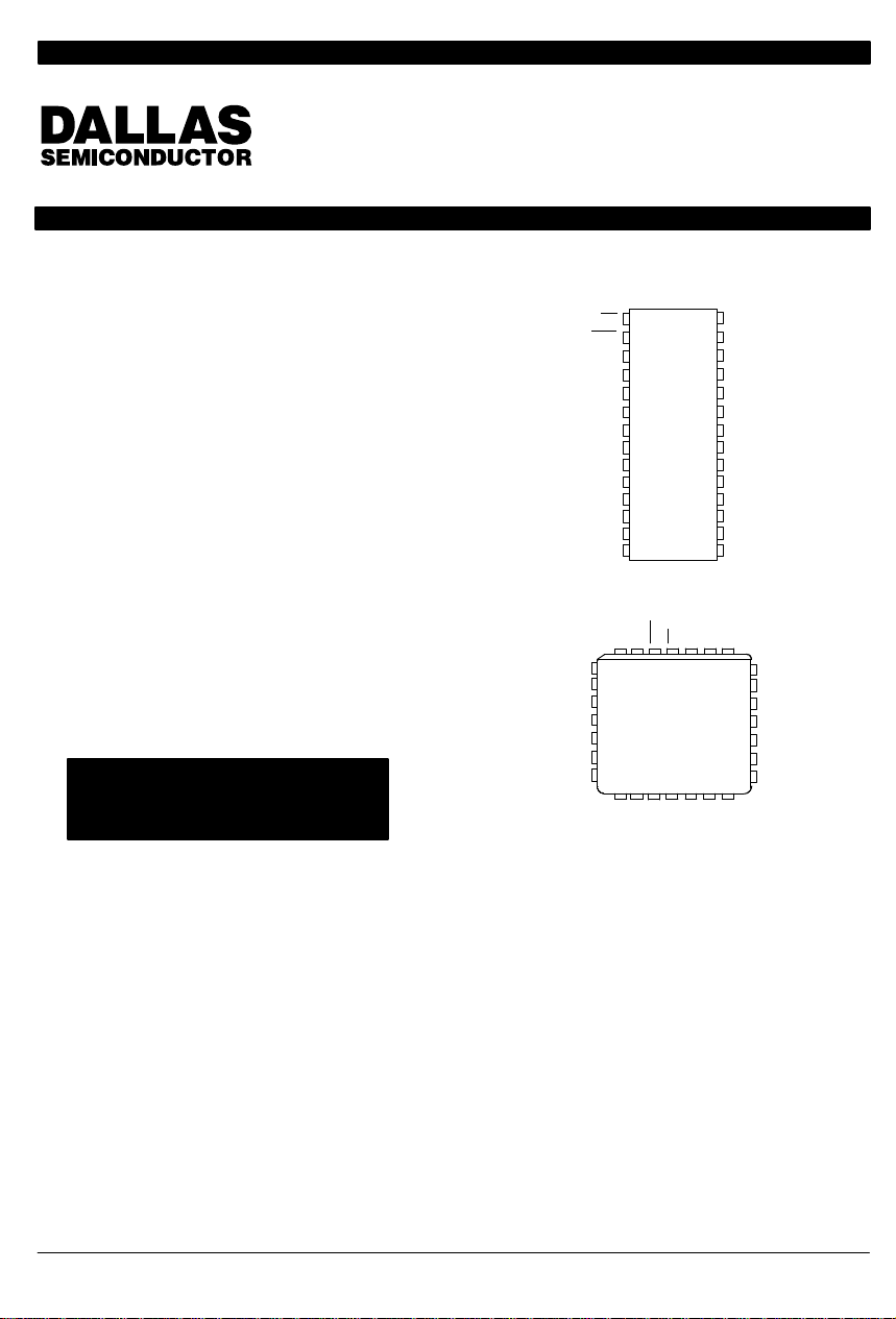
• 28-pin DIP or PLCC (DS2132AQ) packages
There is a series of Application Notes
that accompany this data sheet.
DESCRIPTION
The DS2132A Digital Answering Machine Processor is
a Digital Signal Processor (DSP) optimized for the compression/expansion of PCM coded voice to/from an extremely low bit rate. The DS2132A contains two advanced speech compression algorithms that offer
outstanding fidelity . The Standard Record/Playback algorithm compresses speech to 9.8Kbps and the Extended Record/Playback algorithm compresses
speech to 4.9Kbps.
The DS2132A is ideal for embedded applications such
as digital answering machines, voice mail, voice annunciators, and any other device that needs to maximize
speech storage in a limited memory space. A simple
PIN ASSIGNMENT
600 MIL
RSTNCVCC
GND
1
GND
MCLK
PLCC
PD
28
27
26
25
24
23
22
21
20
19
18
17
16
15
272826
CDIN
VCC
PCMIN
CLK
FS
PCMOUT
TRI_IN
GND
GND
CDOUT
TRI_OUT
FS
CLK
CDIN
PCMINCLK
CLK
25
24
23
22
21
20
19
FS
FS
PCMOUT
TRI_IN
GND
GND
CDOUT
TRI_OUT
PD
1
RST
2
GND
3
GND
4
PD
5
6
VCC
7
VCC
8
VCC
9
VCC
10
VCC
11
VCC
12
GND
13
MCLK
14
GND NC
DS2132A 28-PIN DIP
GND
PD
432
5
6
VCC
7
VCC
8
VCC
9
VCC
VCC
10
VCC
11
12 1314 15 16 1718
GND
DS2132AQ 28-PIN
three wire interface to the embedded microcontroller
frees up valuable controller port pins for other uses and
simplifies the software needed to transfer speech data,
issue commands, and receive DTMF/energy level/status information. The DS2132A detects and generates
all 16 DTMF tones and can also generate a wide variety
of call progress tones. In addition, the DS2132A provides CCITT Rec. T .30 FAX calling tone detection which
enables the answering machine to determine if the incoming call is a voice or FAX transmission. The energy
level detector allows the microcontroller to perform call
progress detection and automatic gain control functions.
Copyright 1995 by Dallas Semiconductor Corporation.
All Rights Reserved. For important information regarding
patents and other intellectual property rights, please refer to
Dallas Semiconductor data books.
041295 1/17
Page 2
DS2132A/Q
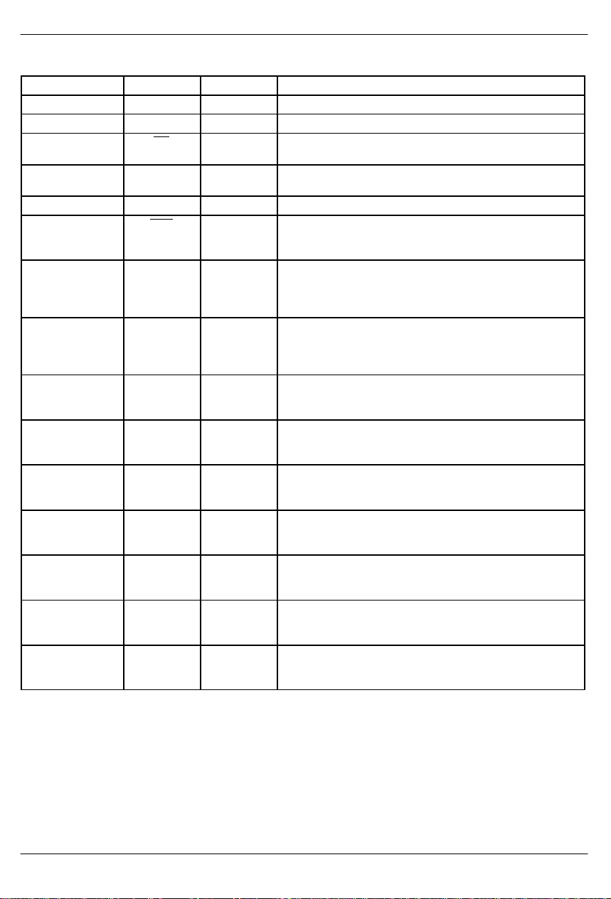
PIN DESCRIPTION Table 1
PIN SYMBOL TYPE DESCRIPTION
3,4,12,14,21,22 GND - Ground. Tie to system ground.
6,7,8,9,10,11,28 VCC - Positive Supply. Tie to system +5 volt supply.
1 PD O Power-Down Active Low. Will toggle low during Power-
5 PD O Power-Down Active High. Will toggle high during Power-
15 NC - No Connect. Do not connect any signal to this pin.
2 RST I Reset. When this pin is low, the internal DSP algorithm is
13 MCLK I Master Processing Clock. The clock used for the internal
16 CDIN I Compressed Data Port Input. Serial input for com-
17,26 CLK I Clock. This clock is used to sample data at CDIN and
18,25 FS I Frame Sync. This input must be an 8 KHz clock with a
19 TRI_OUT O CDOUT Tri-state Control Out. This output should be tied
20 CDOUT O Compressed Data Port Output. Serial output for com-
23 TRI_IN I CDOUT Tri-state Control In. This input should be tied to
24 PCMOUT O PCM Port Output. Output for expanded data which is in
27 PCMIN I PCM Port Input. Input for the 8-bit serial µ-law PCM data
Down mode.
Down mode.
in a reset state. On power-up, this pin should be held low
for at least 100 ms after MCLK is stable.
DSP engine. Should be in the range of 12 to 16 MHz.
MCLK can be asynchronous to any other clock signal on
the DS2132A. The duty cycle should be 50% (±5%).
pressed audio data or DS2132A commands. Samples on
the falling edges of CLK. The compressed data is expanded to 8-bit PCM which is output on PCMOUT.
PCMIN and output data at CDOUT and PCMOUT. CLK
must be synchronous with FS. See Figure 3.
pulse width high time of one to nine CLK cycles for proper
operation. See Figure 3.
to the TRI_IN pin (pin 23) for proper operation; will be low
when CDOUT is active.
pressed audio data or status information, updated on the
rising edge of CLK.
the TRI_OUT pin (pin 19) for proper operation. If this pin is
forced high, CDOUT will not go active.
the standard 8-bit µ-law format. Data is updated on the
rising edges of CLK.
which would normally be supplied by a codec/filter device.
Data is sampled on the falling edges of CLK.
FUNCTIONAL DESCRIPTION
A typical digital answering machine using the DS2132A
is shown in Figure 1. The system consists of a standard
telephone CODEC (COder-DECoder) device, the
DS2132A, a microcontroller , and a bank of DRAM. The
implementation shown is with a Hitachi CODEC and a
8051-type microcontroller but a wide variety of
041295 2/17
CODECs and microcontrollers can be used with the
DS2132A. It is only important that the CODEC have serial digital I/O and have µ-law (“Mu” law) companding.
Table 2 lists some CODECs that will work with the
DS2132A. There is a separate Application Note that explains how to connect these CODECs to the DS2132A.
Page 3
TYPICAL DIGITAL ANSWERING SYSTEM Figure 1
CODEC/FILTER
To 2- to 4–wire
converter and phone line
interface
GA1
GA2
AIN
AOUT
DGND
AGND
PD
Note:
HD44238P is a Hitachi CODEC
12 MHz to 16 MHz
VSS
VDD
PCMOUT
PCMIN
TXCLK
RXCLK
TXSYNC
RXSYNC
-5V
+5V
TXD
8051-Type
Microcontroller
P1.1
+5V
P1.0
+5V
RXD
DS2132A
PCMIN
PCMOUT
CLK
CLK
FS
FS
CDOUT
CDIN
PD
MCLK
RST
TRI_OUT
TRI_IN
VCC
GND
DRAM Array
DS2132A/Q
POR
+5V
RECOMMENDED DS2132A CODECS Table 2
Vendor Model(s)
Texas Instruments TCM29CXX
National Semiconductor TP3054X
Motorola MC1455XX
SGS–Thomson ETC505X
Hitachi HD44238C
As shown in Figure 1, the microcontroller creates the
clock (CLK) and frame sync (FS) that is sent to both the
CODEC and the DS2132A. In this manner, the
DS2132A shares the signals necessary to drive the CODEC. T o “record” an audio signal, the following occurs.
The analog signal applied at the AIN pin of the CODEC
is converted to eight bit values and output at PCMOUT
every 125 µs. The DS2132A takes these eight bit samples in at the PCMIN pin and effectively compresses
them to either 9.8Kbps or 4.9Kbps. See Figure 2. The
compressed data is then passed to the microcontroller
via the CDOUT pin (CD stands for Compressed Data).
The microcontroller then stores the compressed
speech in the DRAM array. The inverse of this process
is required to “playback” the message at the AOUT pin
of the CODEC.
041295 3/17
Page 4
DS2132A/Q
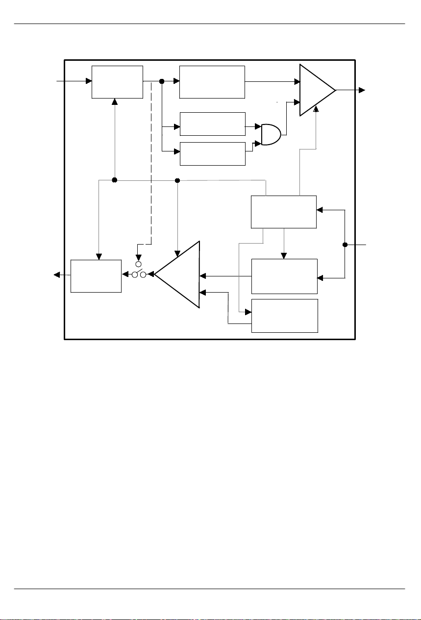
DS2132A BLOCK DIAGRAM Figure 2
PCMIN
PCMOUT
To CODEC
“PCM” Side
Record
Gain Control
Playback
Gain Control
Loopback
DTMF/Level/
FAX Tone
Detection
Threshold
Speech
Compression
Command
Processor
Speech
Expansion
DTMF/Musical
Tone
Generation
CDOUT
T o Microcontroller
“Compressed Data” Side
CDIN
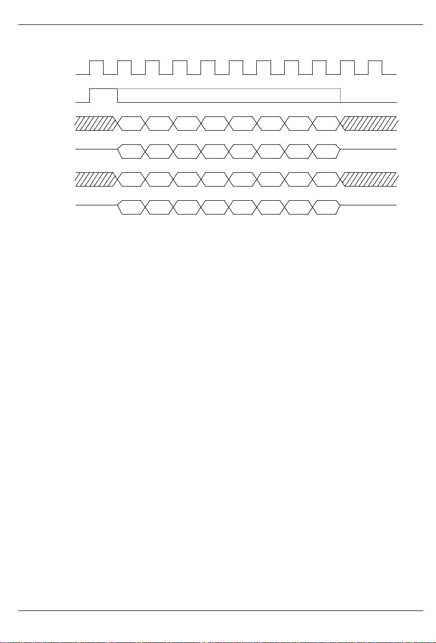
OPERATION OF THE CD AND PCM PORTS
As mentioned earlier, the DS2132A essentially contains
two separate serial ports, one for the DS2132A to microcontroller interface (the CD Port ) and one for the CODEC to DS2132A interface (the PCM Port). The Compressed Data (CD) Port is used to send compressed
speech information from the DS2132A to the microcontroller and vice versa. The CD Port is also used to monitor the current status of the DS2132A and it is used to
issue instructions to the DS2132A. The CD Port consists of the CDIN, CDOUT , CLK, and FS pins (the CLK
041295 4/17
and FS pins are shared with the CODEC). The PCM
Port is used to transfer uncompressed speech data between the DS2132A and the CODEC. It consists of the
PCMIN, PCMOUT, CLK, and FS pins. Figure 3 details
the DS2132A CD and PCM port signals. All communication begins with the frame sync (FS) signal. It indicates to the DS2132A and the CODEC that a byte of information will follow. Note that the PCM Port operates
on a MSB first basis and the CD Port operates on a LSB
first basis.
Page 5
CD & PCM PORT I/O DIAGRAM Figure 3
1
CLK
2
FS
PCMIN
PCMOUT
CDIN
CDOUT
MSB LSB
MSB LSB
LSB MSB
LSB MSB
NOTES:
1. The CLK period must be between 128 KHz and 4.096 MHz
2. The FS pulse must be between 1 and 9 (inclusive) CLK periods long
DS2132A/Q
3-STATE
3-STATE
On the PCM Port, data will be transferred from the CODEC to the DS2132A via one path and transferred from
the DS2132A to the CODEC via another path. These
transfers take place every 125 µs (as determined by the
FS signal). Although the CD Port also transfers data every 125 µs, it operates much differently than does the
PCM Port. The CD Port constantly toggles back and
forth in its data transfer direction. During one frame
sync, the microcontroller will transfer either compressed speech data or command information to the
DS2132A and during the next frame sync, the transfer
direction will switch and the DS2132A will send either
compressed speech data or status information to the
microcontroller. Hence, the CD Port is truly bidirectional. See Figure 4.
041295 5/17
Page 6
DS2132A/Q
CD PORT FLOW STRUCTURE Figure 4
Tone Generation or Idle Recording Mode Playback Mode
CD Port CD Port CD Port
cmd.
status*
cmd.
data
cmd.
status
cmd.
status*
cmd.
data
cmd.
status
DS2132
Microcontroller
DS2132
cmd.
status
cmd.
status
cmd.
status
cmd.
status
cmd.
status
cmd.
status
DS2132
Microcontroller
NOTE: Status Bytes marked with an asterisk (*) indicate bytes with the MSB set to 1.
CD PORT I/O STRUCTURE Figure 5
cmd.
status*
data
status
cmd.
status
cmd.
status
cmd.
status*
data
status
Microcontroller
Tone Generation or Idle
FS
CDIN
CDOUT
Record Mode
FS
CDIN
CDOUT
command
Playback Mode
FS
CDIN
CDOUT
command
command
command command
status status status
command
status*
command data
status status* status
data
command
status
041295 6/17
Page 7

DS2132A/Q
There are three types of bytes that can be transferred on
the CD Port; Command Bytes, Status Bytes, and Compressed Speech Data Bytes (or simply Data Bytes).
The Command Bytes are always transferred from the
microcontroller to the DS2132A to instruct the processor to perform a particular task like transmit a tone. All of
the possible commands that can be sent to the
DS2132A are listed in T able 3. Status Bytes are always
transferred from the DS2132A to the microcontroller.
They inform the microcontroller if a DTMF digit is being
STATUS BYTE FORMAT Figure 6
(MSB)
L4
CDFA DV FCNG
0
FAX Calling Tone Detect
0 = 1100 Hz tone not present
1 = 1100 Hz tone present
DTMF Digit Valid
0 = no DTMF digit detected; received energy level reported at L0 to L4 bits
1 = DTMF digit detected; the digit is reported at D0 to D3 bits
received, or what the current energy level is. See Figure
6. Finally, there are Data Bytes which are transferred
from the DS2132A to the microcontroller during a “recording” and from the microcontroller to the DS2132A
during a “playback”. See Figure 5. When recording, the
microcontroller must read the MSB of the Status Byte to
discriminate between Data Bytes and Status Bytes.
When playing back, the microcontroller must read the
MSB of the Status Byte to know when to send a Command Byte and when to send a Data Byte.
(LSB)
L3
D3
L2
D2
L1
D1
L0
D0
DV = 0
(see Table 4)
DV = 1
(see Table 5)
Compressed Data Frame Alert
Record Mode:
Playback Mode:
Tone Generation or Idle: Will always be set to 0.
0 = next CD Port output is a Status Byte
1 = next CD Port output is a Data Byte
0 = next CD Port input is a Command Byte
1 = next CD Port input is a Data Byte
SYNCHRONIZING THE CD PORT
On power-up, the first task of the microcontroller is to
“synchronize” the CD Port. It can accomplish this by listening to what the DS2132A is sending it. On power-up
(after the RST pin is returned high), the DS2132A will be
in the Idle mode awaiting a command from the microcontroller. Hence it will be alternately sending a Status
Byte to the microcontroller and taking in a Command
Byte. In Figure 1, there is a pull-up resistor on the CD
Port to insure that on power-up, the microcontroller will
send the “no update” command to the DS2132A, which
is [FF]. When the microcontroller reads a value other
than [FF], then it knows that the byte it just read is a Status Byte and hence it will then know that the next byte
will be a Command Byte and it will be synchronized.
RECORD & PLAYBACK MODES
Figure 7 shows two brief flowcharts on what actions the
microcontroller would follow to instruct the DS2132A to
compress (Record Mode) or expand speech (Playback
Mode) data. Before a recording or a playback is to begin, it is recommended that the microcontroller first set
the gain to a nominal position. Then, if needed, the gain
can be adjusted as the recording or playback is occurring. For example, as the recording process begins, the
microcontroller can monitor the incoming speech energy levels via the Status Byte. If the incoming speech level is too low or too high, the gain can be adjusted accordingly. The microcontroller can exit the Recording or
Playback Modes by sending the Idle command.
041295 7/17
Page 8

DS2132A/Q
RECORD & PLAYBACK FLOWCHARTS Figure 7
Record Flowchart Playback Flowchart
Write Command Byte
to set the gain
Read Status Byte
Write Command Byte
to begin recording
Read Status Byte;
does MSB = 1?
Write Command
Byte
Write Command
Byte
Read Data Byte
Write Command
Byte
Write Command Byte
to set the gain
Read Status Byte
Write Command Byte
to begin playback
Read Status Byte;
does MSB = 1?
no yesno yes
Byte
Write Data ByteWrite Command
LOOPBACK MODE
The DS2132A contains a Loopback Mode that is useful
in debugging the CODEC to DS2132A interface and in
adjusting the analog circuits to the proper gain/attenuation levels. In the Loopback Mode, the DS2132A routes
the incoming digitized audio signal received at the
PCMIN pin, back to the PCMOUT pin after making gain
adjustments. See Figure 2. Notice that the route includes the record and playback gain circuits. The Loopback mode can be enabled at any time. When the Loopback is enabled, the generated tones or expanded
speech are ignored. See Figure 2. The DS2132A will
enter the Loopback mode if a Command Byte of [08] is
sent to it by the microcontroller. The Loopback mode
will be exited upon receiving the Exit Loopback Mode
command.
FAX CALLING TONE DETECT
According to CCITT Recommendation T .30, originating
automatic FAX machines should transmit an 1100 Hz
tone for 0.5 seconds every 3.5 seconds (on for 0.5’s; off
for 3.0’s). This tone is meant as an indication to the
called station that a non-voice instrument is making the
call. The Status Byte in the DS2132A reports if a
1100 Hz tone is being received. This detection can be
used to determine if a FAX machine has called the answering machine. The answering machine will then
know not to record the incoming call and to route the call
to a FAX machine.
041295 8/17
Page 9

COMMAND BYTE OPTIONS Table 3
[FF] No update
[00] No update
[BE] Idle
[08] Enter Loopback mode
[09] Exit Loopback mode
[04] Enter Power-Down mode
[05] Exit Power-Down mode
[4A] Set recording path gain to +30 dB
[49] Set recording path gain to +27 dB
[48] Set recording path gain to +24 dB
[47] Set recording path gain to +21 dB
[46] Set recording path gain to +18 dB
[45] Set recording path gain to +15 dB
[44] Set recording path gain to +12 dB
[43] Set recording path gain to +9 dB
[42] Set recording path gain to +6 dB
[41] Set recording path gain to +3 dB
[40] Set recording path gain to 0 dB
[5F] Set recording path gain to -3 dB
[5E] Set recording path gain to -6 dB
[5D] Set recording path gain to -9 dB
[5C] Set recording path gain to -12 dB
[5B] Set recording path gain to -15 dB
[5A] Set recording path gain to -18 dB
[59] Set recording path gain to -21 dB
[58] Set recording path gain to -24 dB
[57] Set recording path gain to -27 dB
[56] Set recording path gain to -30 dB
[80] Generate DTMF “0” (941+1336 Hz)
[81] Generate DTMF “1” (697+1209 Hz)
[82] Generate DTMF “2” (697+1336 Hz)
[83] Generate DTMF “3” (697+1477 Hz)
[84] Generate DTMF “4” (770+1209 Hz)
[85] Generate DTMF “5” (770+1336 Hz)
[86] Generate DTMF “6” (770+1477 Hz)
[87] Generate DTMF “7” (852+1209 Hz)
[90] Generate Dial tone (350+440 Hz)
[91] Generate Ringing tone (480+440 Hz)
[94] Generate bright musical note “A” (440+1320 Hz)
[95] Generate bright musical note “B” (494+1482 Hz)
[96] Generate bright musical note “C” (523+1569 Hz)
[97] Generate bright musical note “D” (587+1761 Hz)
[97] Generate bright musical note “D” (587+1761 Hz)
[98] Generate bright musical note “E” (659+1977 Hz)
[99] Generate bright musical note “F” (698+2094 Hz)
[9A] Generate bright musical note “G” (784+2352 Hz)
[B4] Generate musical note “A” (440 Hz)
[B5] Generate musical note “B” (494 Hz)
[B6] Generate musical note “C” (523 Hz)
[B7] Generate musical note “D” (587 Hz)
DS2132A/Q
[B8] Generate musical note “E” (659 Hz)
[B9] Generate musical note “F” (698 Hz)
[BA] Generate musical note “G” (784 Hz)
[9B] Generate bright musical note “A” one octave
higher (880+2640 Hz)
[9C] Generate bright musical note “B” one octave
higher (988+2974 Hz)
[BB] Generate musical note “A” one
octave higher (880 Hz)
[BC] Generate musical note “B” one octave
higher (988 Hz)
[25] Record at Standard rate (9.8Kbps)
[27] Record at Extended rate (4.9Kbps)
[28] Playback at Standard rate (9.8Kbps)
or Premium Rate (16Kbps) with echo
cancellation enabled
[2A] Playback at Extended rate (4.9Kbps)
or Intermediate Rate (8Kbps) with echo
cancellation enabled
[23] Record at Intermediate rate (8Kbps)
[21] Record at Premium rate (16Kbps)
[20] Playback at Standard rate (9.8 Kbps) or
Premium rate [16Kbps] with echo
cancellation disabled
[22] Playback at Extended rate (4.9Kbps) or
Intermediate rate (8Kbps) with echo
cancellation disabled
[6A] Set playback path gain to +30 dB
[69] Set playback path gain to +27 dB
[68] Set playback path gain to +24 dB
[67] Set playback path gain to +21 dB
[66] Set playback path gain to +18 dB
[65] Set playback path gain to +15 dB
[64] Set playback path gain to +12 dB
[63] Set playback path gain to +9 dB
[62] Set playback path gain to +6 dB
[61] Set playback path gain to +3 dB
[60] Set playback path gain to 0 dB
[7F] Set playback path gain to -3 dB
[7E] Set playback path gain to -6 dB
[7D] Set playback path gain to -9 dB
[7C] Set playback path gain to -12 dB
[7B] Set playback path gain to -15 dB
[7A] Set playback path gain to -18 dB
[79] Set playback path gain to -21 dB
[78] Set playback path gain to -24 dB
[77] Set playback path gain to -27 dB
[76] Set playback path gain to -30 dB
[88] Generate DTMF “8” (852+1336 Hz)
[89] Generate DTMF “9” (852+1477 Hz)
041295 9/17
Page 10

DS2132A/Q
[8A] Generate DTMF “A” (697+1633 Hz)
[8B] Generate DTMF “B” (770+1633 Hz)
[8C] Generate DTMF “C” (852+1633 Hz)
[8D] Generate DTMF “D” (941+1633 Hz)
[8E] Generate DTMF “*” (941+1209 Hz)
[8F] Generate DTMF “#” (941+1477 Hz)
[92] Generate Busy tone (480+620 Hz)
[93] Generate 400 Hz tone
[9E] Generate 1004 Hz tone
[9D] Generate 1400 Hz tone
[10] Set “off” threshold to -50 dBm
[11] Set “off” threshold to -49 dBm
[12] Set “off” threshold to -47dBm
[13] Set “off” threshold to -44 dBm
[14] Set “off” threshold to -42 dBm
[15] Set “off” threshold to -40 dBm
[16] Set “off” threshold to -38 dBm
[17] Set “off” threshold to -35 dBm
[18] Set “off” threshold to -32 dBm
[19] Set “off” threshold to -29 dBm
[1A] Set “off” threshold to -26 dBm
[1B] Set “off” threshold to -23 dBm
[1C] Set “off” threshold to -20 dBm
[1D] Set “off” threshold to -17 dBm
[1E] Set “off” threshold to -14 dBm
[1F] Set “off” threshold to -11 dBm
NOTES:
1. All tones are generated at 0 dBm0 except for the high tones of DTMF which are at +3 dBm0.
2. The unit dBm0 represents a digital representation of an analog level; throughout this data sheet, the zero
reference point of 0 dBm0 was measured with a Hitachi HD44238P CODEC which produces a 1.231Vrms
analog signal when sent a “0 dBm0” digital code.
3. All letters and numbers contained in brackets ([ ]) represent Hexadecimal values.
4. The above hexadecimal code are sent LSB first.
041295 10/17
Page 11

DS2132A/Q
DEFINITION OF THE L0 TO L4 LEVEL BITS
Table 4
L4 L3 L2 L1 L0 ENERGY LEVEL
RECEIVED
0 0 0 0 0 <-48dBm0
0 0 0 1 0 -45dBm0
0 0 1 0 0 -42dBm0
0 0 1 0 1 -39dBm0
0 0 1 1 0 -36dBm0
0 0 1 1 1 -33dBm0
0 1 0 0 0 -30dBm0
0 1 0 0 1 -27dBm0
0 1 0 1 0 -24dBm0
0 1 0 1 1 -21dBm0
0 1 1 0 0 -18dBm0
0 1 1 0 1 -15dBm0
0 1 1 1 0 -12dBm0
0 1 1 1 1 -9dBm0
1 0 0 0 0 -6dBm0
1 0 0 0 1 -3dBm0
1 0 0 1 0 0dBm0
1 0 0 1 1 +3dBm0
1 0 1 0 0 +6dBm0
1 0 1 0 1 +9dBm0
DEFINITION OF THE D0 TO D3 DTMF BITS
Table 5
D3 D2 D1 D0 DTMF DIGIT
DETECTED
0 0 0 0 DTMF Digit “0”
0 0 0 1 DTMF Digit “1”
0 0 1 0 DTMF Digit “2”
0 0 1 1 DTMF Digit “3”
0 1 0 0 DTMF Digit “4”
0 1 0 1 DTMF Digit “5”
0 1 1 0 DTMF Digit “6”
0 1 1 1 DTMF Digit “7”
1 0 0 0 DTMF Digit “8”
1 0 0 1 DTMF Digit “9”
1 0 1 0 DTMF Digit “A”
1 0 1 1 DTMF Digit “B”
1 1 0 0 DTMF Digit “C”
1 1 0 1 DTMF Digit “D”
1 1 1 0 DTMF Digit “*”
1 1 1 1 DTMF Digit “#”
POWER-DOWN MODE
The DS2132A can be placed into a low-power standby
condition by sending the enter power-down command
[04] to the DS2132A. The DS2132A will power down
within 500 µs after receiving the power-down command.
The MCLK signal should still be applied to the DS2132A
in the power-down mode. The CLK and FS signals may
be either stopped or continued. In the power-down
mode, the DS2132A will consume about 1 mA and the
pin (Pin 1) will be forced low and the PD pin (Pin 5)
PD
will be forced high. The PD
power-down the CODEC. See Figure 2. T o exit the power-down mode, the exit power-down command [05]
should be sent to the DS2132A. There is no need to issue a hardware reset via the RST
set itself. The DS2132A will power-up in the Idle mode.
The microcontroller should wait 1 ms after issuing the
exit power-down command before reinitializing the
device.
and PD pins can be used to
pin; the device will re-
041295 11/17
Page 12

DS2132A/Q
ABSOLUTE MAXIMUM RATINGS*
Voltage on Any Pin Relative to Ground -1.0V to +7.0V
Operating Temperature 0°C to 70°C
Storage Temperature -55°C to +125°C
Soldering Temperature 260°C for 10 seconds
* This is a stress rating only and functional operation of the device at these or any other conditions above
those indicated in the operation sections of this specification is not implied. Exposure to absolute maximum rating conditions for extended periods of time may affect reliability.
RECOMMENDED DC OPERATING CONDITIONS (0°C to 70°C)
PARAMETER SYMBOL MIN TYP MAX UNITS NOTES
Logic 0 V
Logic 1 V
Supply V
IL
IH
CC
-0.3 0.8 V
2.0 VCC +0.3 V
4.5 5.5 V
CAPACITANCE (tA = 25°C)
PARAMETER SYMBOL MIN TYP MAX UNITS NOTES
Input Capacitance C
Output Capacitance C
IN
OUT
5 pF
10 pF
DC ELECTRICAL CHARACTERISTICS (0°C to 70°C; VCC = 5V + 10%)
PARAMETER SYMBOL MIN TYP MAX UNITS NOTES
Active Supply Current I
Input Leakage I
Output Leakage I
Output Current (2.4 V) I
Output Current (0.4V) I
Power-Down Current I
DDA
LI
LO
OH
OL
PD
-1.0 +1.0 µA
-1.0 -1.0 µA 3
-1.0 -1.0 mA
+4.0 mA
35 40 mA 1,2
1 mA 1,2,4
NOTES:
1. VCC = 5.5V; CLK=2.048 MHz; MCLK=16 MHz.
2. Outputs open; inputs swinging full supply levels.
3. PCMOUT and CDOUT are 3-stated.
4. Power-down mode.
041295 12/17
Page 13

DS2132A/Q
DTMF RECEIVER CHARACTERISTICS (0°C to 70°C; VCC = 5V + 10%)
PARAMETER SYMBOL MIN TYP MAX UNITS NOTES
Valid Detect Amplitude Range -40 0 dBm0 1,2
Frequency Deviation Accept + 1.5 % 3
Frequency Deviation Reject +3.5 % 3
Minimum Twist Accept Range -10 +10 dB 4
Talk Off (Mitel Tape CM7291) 5 Hits 5
Noise Tolerance (Mitel Test Tape
CM7291)
-12 dB 6
NOTES:
1. 0 dBm0 = 1.231Vrms when sent through a Hitachi HD44238P CODEC as shown in Figure 1.
2. Individual tone level of the DTMF pair with recording path gain set to 0db.
3. Percent of nominal frequency for the individual tone; FS = 8 KHz (+
4. Twist = 20 LOG (High tone/Low tone).
5. Talk Off is a measure of the speech immunity of a DTMF receiver; the lower the number of hits, the better the
immunity .
6. Three KHz bandlimited white noise, referenced to lowest amplitude in the DTMF pair.
0.1%).
DTMF DETECTION TIMING (0°C to 70°C; VCC = 5V + 10%)
PARAMETER SYMBOL MIN TYP MAX UNITS NOTES
Tone Duration Accept 40 ms
Tone Duration Reject 20 ms
Interdigit Pause Accept 40 ms
Interdigit Pause Reject 20 ms
DTMF TONE GENERATOR CHARACTERISTICS (0°C to 70°C; VCC = 5V + 10%)
PARAMETER SYMBOL MIN TYP MAX UNITS NOTES
DTMF Frequency Deviation (each
tone of the pair)
Output Distortion (single tone) -25 dB 2
DTMF Tone Level Twist +3 dB 3
+1.0 % 1
NOTES:
1. FS = 8.0 KHz + 0.1%
2. Total harmonic distortion relative to test tone signal.
3. Twist = 20 LOG (High tone/Low tone).
041295 13/17
Page 14

DS2132A/Q
DATA INPUT/OUTPUT
AC ELECTRICAL CHARACTERISTICS (0°C to 70°C; V
PARAMETER SYMBOL MIN TYP MAX UNITS NOTES
CLK Clock Period t
CLK Pulse Width High, Low tWH, t
CLK Rise, Fall Times tR, t
Hold Time from CLK to FS t
HOLD
Setup Time from FS high CLK low t
Hold Time from CLK low to FS
t
low
Setup Time from PCMIN, CDIN to
CLK low
Hold Time from PCMIN, CDIN to
CLK low
Delay Time from CLK to Valid
PCMOUT, CDOUT
Delay Time from CLK to
t
SD
t
HD
t
DO
t
PCMOUT, CDOUT 3-stated
P
WL
F
SF
HF
DZ
244 7813 ns 1,2
100 ns 2
20 ns 2
0 ns 2
50 ns 2
100 ns 2
50 ns 2
50 ns 2
10 150 ns 2
20 150 ns 2
= 5V + 10%)
CC
NOTES:
1. At least nine CLK clocks must be received within first half of the FS period (62.5 µs).
2. See Figure 8.
MASTER CLOCK/RESET
AC ELECTRICAL CHARACTERISTICS (0°C to 70°C; V
PARAMETER SYMBOL MIN TYP MAX UNITS NOTES
MCLK Period t
PM
MCLK Duty Cycle 45 55 %
MCLK Rise/Fall Times tRM, t
RST Pulse Width t
FM
RST
62 84 ns 1,2
10 ns 2
100 ms 2
= 5V + 10%)
CC
NOTES:
1. MCLK = 12 to 16 MHz.
2. See Figure 9.
041295 14/17
Page 15

DS2132A/Q
DATA I/O AC TIMING DIAGRAM Figure 8
CLK
FS
PCMIN,
CDIN
PCMOUT
CDOUT
t
HOLD
3-STATE
t
R
t
SF
t
HF
t
F
MSB for PCMIN
LSB for CDIN
MSB for PCMOUT
LSB for CDOUT
t
DO
MASTER CLOCK & RESET AC TIMING DIAGRAM Figure 9
t
RM
t
FM
t
P
t
WH
t
SD
t
WMH
t
WL
t
HD
t
DZ
t
PM
t
WML
MCLK
RST
t
RST
041295 15/17
Page 16
DS2132A/Q
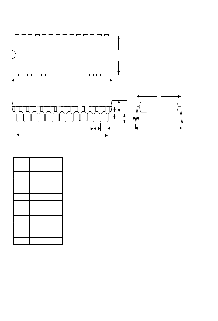
DS2132A DIGITAL ANSWERING MACHINE PROCESSOR
28 15
B
1
13 EQUAL SPACES AT + .010
INCHES
DIM MIN MAX
A 1.445 1.470
B 0.530 0.550
C 0.140 0.160
D 0.600 0.625
E 0.015 0.040
F 0.120 0.145
G 0.090 0.1 10
H 0.600 0.680
J 0.008 0.012
K 0.015 0.022
A
TNA
14
D
C
E
GK
F
J
H
041295 16/17
Page 17

DS2132AQ DIGITAL ANSWERING MACHINE PROCESSOR
E
E1
N
1
CH1
E2
INCHES
DIM MIN MAX
A 0.165 0.180
A1 0.090 0.120
A2 0.020 –
B 0.026 0.033
B1 0.013 0.021
C 0.009 0.012
D 0.485 0.495
D1 0.450 0.456
D2 0.390 0.430
E 0.485 0.495
E1 0.450 0.456
E2 0.390 0.430
L1 0.060 –
N 28 –
e1 0.050 BSC
CH1 0.042 0.048
D1 D D2
e1
DS2132A/Q
B
L1
B1
A
C
A1A2
041295 17/17
 Loading...