

Page 1
DS2130Q
DS2130Q
Voice Messaging Processor
FEATURES
• Per-channel voice messaging processor for digitized
voice storage and retrieval
• High fidelity speech recording and playback at 8, 12,
16, 24 and 32 Kbits/sec
• Integral DTMF transceiver for remote touch-tone con-
trol and dialing
• Connects to popular PCM codec/filters for analog in-
terfacing
• Direct PCM serial data bus interfaces to any of 32 pos-
sible TDM time slots
• Monitors and reports audio energy levels for call prog-
ress and voice detection
• Selectable beep generator for sound prompts
• 3-wire synchronous serial control port
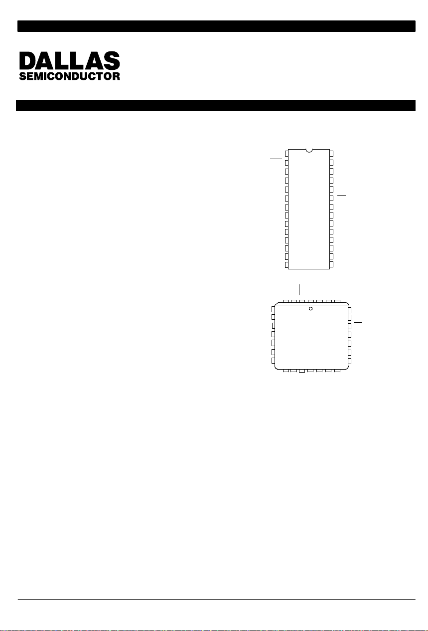
• 28-pin DIP or PLCC (DS2130Q) packages
DESCRIPTION
The DS2130 Voice Messaging Processor is a CMOS
DSP processor that serves as a voice messaging engine for digitized voice storage and retrieval applications. It offers half-duplex speech compression or expansion at either 8, 12, 16, 24 or 32 Kbits/sec. The
advanced speech compression algorithm maintains excellent audio clarity even at low bit rates. The algorithm
also incorporates a DTMF transceiver for decoding or
generating touch-tone signals for remote control and
automatic dialing. The tone generator can be used to
create single-tone beeps used in popular answering
machines. Voice and call progress detection can be
easily implemented using the energy threshold detect
outputs.
PIN ASSIGNMENT
DT1
1
RST
2
TM0
3
TM1
4
DT0
5
A0
6
7
A1
A2
8
A3
9
A4
10
A5
11
SPS
12
MCLK
13
GND
14
TM1
432
5
DT0
6
A0
7
A1
A2
8
9
A3
A4
10
11
A5
12 1314 15 16 1718
MCLK
SPS
The DS2130 can be used together with a low-cost codec/filter device for analog interfacing in standalone
applications such as answering machines or feature
phones. It can also interface directly to a serial PCM bus
on any of up to 32 possible time slots using an internal
software-selectable time slot assigner circuit (TSAC).
This configuration can be used in digital switching systems for adding voice messaging services to existing
backplane designs.
Applications include digital answering machines, embedded voice response, speech annunciators, voice
mail, key telephone systems and automatic operator
services.
TM0
GND
RST
DT3
DT1
CPXIN
28
27
26
25
24
23
22
21
20
19
18
17
16
15
VCC
PCMIN
27 2628
CPXCLK
Vcc
PCMIN
PCMCLK
PCMFS
PCMOUT
CS
SDI
SCLK
CPXOUT
DT2
CPXFS
CPXCLK
CPXIN
DT3
PCMCLK
25
24
23
22
21
20
19
CPXFS
PCMFS
PCMOUT
CS
SDI
SCLK
CPXOUT
DT2
Copyright 1995 by Dallas Semiconductor Corporation.
All Rights Reserved. For important information regarding
patents and other intellectual property rights, please refer to
Dallas Semiconductor data books.
041295 1/22
Page 2
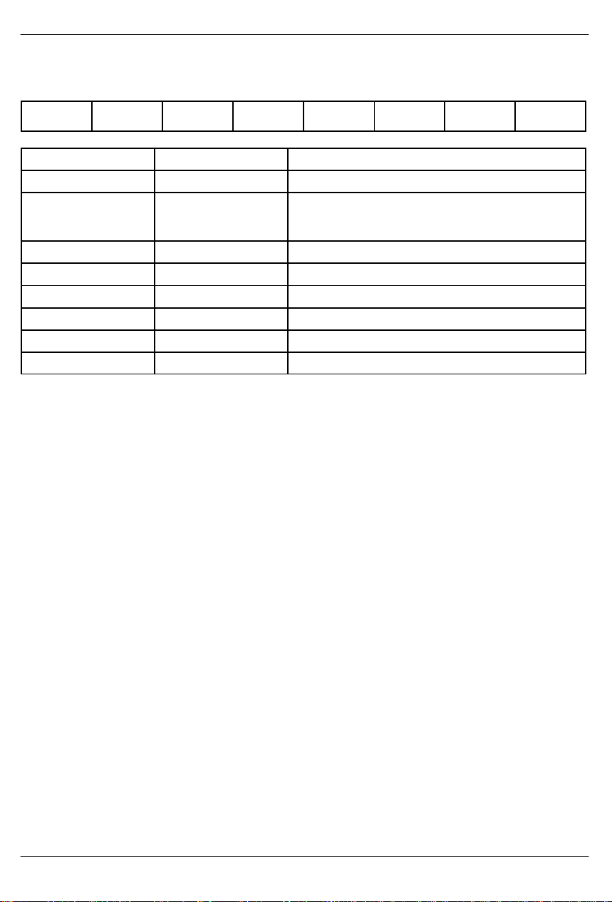
PIN DESCRIPTION Table 1
PIN SYMBOL TYPE DESCRIPTION
5
1
19
15
2 RST I Reset input. When this pin is low, the internal DSP algorithm is in a reset state
3
4
6
7
8
9
10
11
12 SPS I Serial Port Select. This pin must be tied to VCC for proper operation of the serial
13 MCLK I Master processing clock. This is the clock used for the internal DSP engine and
14 GND - Ground. Tie this pin to the system logic ground.
16 CPXIN I Compressed data in. This is the serial data input for the compressed audio data
17 CPXCLK I Compression/expansion side data clock. This is the clock used to sample data
18 CPXFS I Compression/expansion side frame sync. This input must be an 8 KHz clock
20 CPXOUT O Compressed data out. This is the serial data output for the compressed audio
21 SCLK I Serial port clock. This is the clock used to write configuration data to the serial
22 SDI I Serial data input. Data source for the serial port registers.
23 CS I Chip select input. This pin must transition high to low before each write operation
24 PCMOUT O PCM output. This is the output for expanded data which is in the standard 8-bit
DT0
DT1
DT2
DT3
TM0
TM1
A0
A1
A2
A3
A4
A5
O
Detect outputs 0-3. These are the four output detect lines that report energy
O
threshold levels and DTMF tones. DTMF tone detection always has precedence
O
over energy level reporting.
O
for proper initialization. The DS2130 should always be reset for at least
1 ms after each power-up occurrence.
IITest mode pins. These pins are used for factory testing and must be tied to GND
for proper operation.
I
Address Select. Provides serial address ID of the DS2130. The states of A0-A5
I
must match the address sent in the command byte to enable the serial port. A0
I
= LSB.
I
I
I
port. The hardware mode is not
supported on the DS2130.
should be in the range of 10.5 - 13 MHz. MCLK can be asynchronous to any other
clock signal on the DS2130. The duty cycle should be nominally 50%.
sampled on falling edges of CPXCLK during selected time slots. This data is expanded to 8-bit PCM that is output on PCMOUT except in PCM bypass mode.
at CPXIN, to output data at CPXOUT and to determine the proper time slot.
CPXCLK must be synchronous with CPXFS. See “Special Clock Requirements”
section for more details.
for proper operation. CPXFS must be the same frequency as PCMFS (normally
they are tied together).
data, updated on rising edges of CPXCLK during selected time slots.
port registers.
to the serial port.
PCM u/A-law format. Data is updated on rising edges of PCMCLK.
DS2130Q
041295 2/22
Page 3

DS2130Q
PIN DESCRIPTIONTYPESYMBOL
25 PCMFS I PCM side frame sync. An 8 KHz clock signal must be applied for the PCM data
interface. Lower sample rates can be used to reduce the effective bit rate but may
result in unusable DTMF detection and generation as well as lower voice quality.
PCMFS is normally tied to CPXFS.
26 PCMCLK I PCM side data clock. This is the clock used to sample PCM serial data at
PCMIN, to output data at PCMOUT and to determine the proper time slot.
PCMCLK must be synchronous with PCMFS.
27 PCMIN I PCM data input. This is the input for the 8-bit serial PCM data which would nor-
mally be supplied by a codec/filter device. Data is sampled on falling edges of
PCMCLK.
28 V
cc
- Positive supply input. Tie to system +5 volt supply.
041295 3/22
Page 4
DS2130 SIGNAL FLOW DIAGRAM Figure 1
DS2130Q
ENERGY
DETECTOR
FILTER
DTMF LOW-BAND
DT0-DT3
MUX
DTMF
DECODER
Valid digit detect
FILTER
DTMF HIGH-BAND
CPXOUT
CPXCLK
COMPRESSION/
AUDIO
(Record)
COMPRESSION
CPXFS
DATA
EXPANSION
INTERFACE
CPXIN
AUDIO
EXPANSION
(Playback)
SPS
SDI
SCLKCSRST
SERIAL PORT
COMP/EXP SELECT
A0-A5
AND
TIMING
CONTROL
INTERFACE
TONE CONTROL
MULTI-TONE
GENERATOR
MCLK
INTERNAL DSP
PROCESSING CLOCK
041295 4/22
PCMIN
PCM
DATA
INTERFACE
PCMCLK
PCMFS
PCMOUT
Page 5
DS2130Q
HARDWARE RESET
RST allows the host to reset the DSP algorithms and
the contents of the serial port control registers. This pin
must be held low for at least 1 ms on system power-up
after MCLK is stable to ensure that the device has initialized properly. RST
clears all bits of both control registers except the CPD1 and CPD2 bits, which are set to
one. However, these bits are ignored until they have
been reset by the host; that is, the DS2130 will not power up in the power-down mode. This permits the host to
communicate through the serial port at full speed after
power-up.
SERIAL PORT CONTROL
An external host controller writes configuration data to
the DS2130 via the serial port through inputs SCLK,
SDI, and CS as shown in Figure 2 (read operations are
not supported). Each write to the DS2130 is either a
2-byte write or a 4-byte write. A 2-byte write consists of
the Address/Command Byte (ACB) followed by a byte
to configure either the Voice Control Register (VCR) or
SERIAL PORT WRITE Figure 2
CS
the T one Control Register (TCR). The 4-byte write consists of the ACB followed by a byte to configure the appropriate control register and then two bytes for input
and output time slot mapping. When writing to the VCR,
the next two bytes program the input and output time
slots respectively for the compression/expansion (CPX)
side interface. When writing to the TCR , the next two
bytes program the input and output time slots respectively for the PCM side interface.
ADDRESS/COMMAND BYTE
The address/command byte is the first byte written to
the serial port; it identifies which of the 64 possible
DS2130’s sharing the serial bus is to be accessed. Address data must match that at inputs A0 to A5. If no
match occurs, the DS2130 ignores the following data at
SDI. If an address match occurs, the next three bytes
written are accepted as control, input and output time
slot data. Bit ACB.6 determines whether the Voice or
Tone Control register is to be updated.
SCLK
SDI
A0 A1 A2 A3 A4
NOTE:
A 2-byte write is shown.
A5 0
ADDRESS/COMMAND CONTROL
CR7CR0V/T
041295 5/22
Page 6
ADDRESS/COMMAND BYTE Figure 3
(MSB) (LSB)
DS2130Q
-
V/T A5 A4 A3 A2 A1 A0
SYMBOL POSITION NAME AND DESCRIPTION
- ACB.7 Reserved; must be zero for proper operation.
V/T ACB.6 Voice/Tone command byte select.
0 = write to Tone Generator Control register
1 = write to Voice Control register
A5 ACB.5 MSB of Device Address.
A4 ACB.4
A3 ACB.3
A2 ACB.2
A1 ACB.1
A0 ACB.0 LSB of Device Address.
VOICE CONTROL REGISTER
The Voice Control Register (VCR) determines the compression/expansion bit rate and PCM data format. It
also provides power-down and algorithm reset control.
The u/A bit selects either µ-law or A-law PCM data encoding for PCMIN and PCMOUT pins. When u/A = 1,
µ-Law is selected; when u/A = 0, A-Law is selected.
Compression or expansion bit rates are determined by
bits CXS1, CXS2 and CXS3. See T able 2 for the mapping of these bits. For the reduced bandwidth modes,
the incoming PCM data is internally filtered with a 1.7
KHz low-pass and sampled at one-half of the CPXFS/
PCMFS frequency. The PCM Bypass mode (CXS1=1,
CXS2=0 and CXS3=1) permits input PCM data at either
PCMIN or CPXIN to be routed out to CPXOUT or
PCMOUT respectively, bypassing normal compression/expansion.
Voice compression/expansion can be disabled by setting CPD1 to a 1. In this mode, the compression/expansion algorithm is idled and CPXOUT is tri-stated. This
mode should be used when only DTMF/tone generation
and detection are desired. When CPD1 and CPD2
(CPD2 is in the Tone Control register) are both equal to a
1, the device enters a low-power standby mode in which
all DSP operation is halted.
must not be operated faster than 39 KHz.
CPXRST resets the algorithm coefficients for the expansion/compression algorithm to their initial values.
CPXRST will be cleared by the device when the algorithm reset is complete.
The compression/expansion loopback feature is enabled when CXLB is set and CPD1 is cleared. During
this loopback, no expansion or compression occurs and
input data at CPXIN is looped back to the appropriate
time slot at CPXOUT.
Compression or expansion operation is selected via the
CP/EX bit (the DS2130 cannot perform both simultaneously).
In this mode, the serial port
041295 6/22
Page 7
DS2130Q
VOICE CONTROL REGISTER Figure 4
(MSB) (LSB)
CP/EX
CXS1 CPD1 CXRST CXLB U/A CXS2 CXS3
SYMBOL POSITION NAME AND DESCRIPTION
CP/EX VCR.7 Compression/expansion select.
1 = compress (record)
0 = expand (playback)
CXS1 VCR.6 Compression/expansion bit rate select 1; see Table 2.
CPD1 VCR.5 Compression/Expansion power-down 1.
0 = Compression/expansion enabled
1 = Compression/expansion disabled
CXRST VCR.4 Compression/expansion algorithm reset.
0 = normal operation
1 = reset algorithm to initial coefficients
CXLB VCR.3 Compression/expansion interface loopback.
0 = normal operation
1 = bypass selected channel
U/A VCR.2 PCM input/output data format.
0 = A-Law
1 = µ-Law
CXS2 VCR.1 Compression/Expansion bit rate select 2; see Table 2.
CXS3 VCR.0 Compression/Expansion bit rate select 3.
COMPRESSION/EXPANSION BIT RATE SELECT Table 2
ALGORITHM SELECTED CXS1 CXS2 CXS3
64Kbps to/from 32Kbps 0 0 0
64Kbps to/from 24Kbps 1 1 0
64Kbps to/from 16Kbps 0 1 0
Reserved for future operation 1 0 0
64Kbps to/from 16Kbps
64Kbps to/from 12Kbps
64Kbps to/from 8Kbps
64Kbps to/from 64Kbps
(PCM Bypass mode)
1
1
1
0 0 1
1 1 1
0 1 1
1 0 1
NOTE:
1. These reduced bandwidth modes use an internal low-pass filter at 1.7 KHz to permit a lower bit rate. The
normal bandwidth otherwise is 300 Hz to 3.4 KHz due to the filters typically present in the codec/filter device
used with the DS2130.
041295 7/22
Page 8

DS2130Q
pp g
TS1
TCR.2
be written
0
CPD1=0 while CPD2=1 should
0
0
TONE CONTROL REGISTER
The Tone Control register provides access to the tone
that DTMF digits be sustained for at least 50 mS for
proper network recognition.
generator and controls power-down and reset functions.
The CPD2 bit is used in conjunction with CPD1 (in the
VCR) to enable a power-down mode in which power
The tone generator is controlled by bits TS0-3, which
cause either transmission of a DTMF digit or one of
three possible single-tone sine waves. The DTMF digits
consumption is reduced to a minimum. CPD1 and
CPD2 must both equal a 1 to enter this mode. The
PCMOUT output is three-stated when CPD2 = 1.
that can be transmitted are 0-9, # and *. The single
tones available are 350, 620 and 1004 Hz, any of which
can be used as beeps for user prompting. T one generation lasts for as long as the particular state is programmed; all tone generation ceases when TS0-3
equal 1111 (the power-up state). When writing a new
value for TS0-3 (including the 1111 state), the TRST bit
must be simultaneously set to a 1; otherwise, the old value of TS0-3 will continue to be used. It is recommended
Testing of the DTMF generation and detection circuitry
can be accomplished by setting TLB to a 1. In this mode,
transmit DTMF tones are internally looped back to the
DTMF receiver for test purposes (the DT0-3 pins can be
monitored for proper operation). Also in this mode, input
PCM data is looped back to the appropriate time slot on
PCMOUT. This permits isolation and testing of the ex-
ternal codec/filter used with the DS2130.
TONE CONTROL REGISTER Figure 5
(MSB) (LSB)
TS3
SYMBOL POSITION NAME AND DESCRIPTION
CPD2 TCR.5
TRST TCR.4
TS2 CPD2 TRST TLB TS1 TS0 -
TS3
TS2
TS1
TS0
TCR.7
TCR.6
TCR.2
TCR.1
Tone selects 0-3. See Table 3 for tone bit mapping.
TRST must be written to a 1 when a new tone value is to
be written.
.
Compression/Expansion power-down 2.
= Normal operation
1 = Power-down all DSP operation. CPD1 must equal 1
grammed.
Tone generation reload enable for TS0-3.
= normal operation/ready for new value
1 = load new tone value
TLB TCR.3
Tone generation loopback.
= normal operation
1 = loopback tone signals to DTMF receiver
- TCR.0 Should always be set to 1.
not be pro-
-as well.
041295 8/22
Page 9

DS2130Q
TONE GENERATION BIT MAPPING1 Table 3
TS3-TS0 SIGNAL LEVEL (dBm0)
0000 DTMF ‘‘0” -3
0001 DTMF ‘‘1” -3
0010 DTMF ‘‘2” -3
0011 DTMF ‘‘3” -3
0100 DTMF ‘‘4” -3
0101 DTMF ‘‘5” -3
0110 DTMF ‘‘6” -3
0111 DTMF ‘‘7” -3
1000 DTMF ‘‘8” -3
1001 DTMF ‘‘9” -3
1010 DTMF ‘‘*” -3
1011 DTMF ‘‘#” -3
1100 1004 Hz 0
1101 350 Hz -12
1110 620 Hz -12
1111 Silence OFF
1. States 0000 through 101 1 generate DTMF digit signals; states 1100, 1101 and 1 110 generate single frequency tones; state 1111 disables all tone generation (DTMF or single tone).
INPUT TIME SLOT REGISTER Figure 6
(MSB) (LSB)
-
SYMBOL POSITION NAME AND DESCRIPTION
D5 ITR.5 MSB of input time slot register.
D4 ITR.4
D3 ITR.3
D2 ITR.2
D1 ITR.1
D0 ITR.0 LSB of input time slot register.
- D5 D4 D3 D2 D1 D0
- ITR.7 Reserved; must be zero for proper operation.
- ITR.6 Reserved; must be zero for proper operation.
041295 9/22
Page 10

OUTPUT TIME SLOT REGISTER Figure 7
(MSB) (LSB)
DS2130Q
-
- D5 D4 D3 D2 D1 D0
SYMBOL POSITION NAME AND DESCRIPTION
- OTR.7 Reserved; must be zero for proper operation.
- OTR.6 Reserved; must be zero for proper operation.
D5 OTR.5 MSB of output time slot register.
D4 OTR.4
D3 OTR.3
D2 OTR.2
D1 OTR.1
D0 OTR.0 LSB of output time slot register.
TIME SLOT ASSIGNMENT/ORGANIZATION
Onboard counters establish when PCM and compression/expansion I/O occurs. The counters are programmed via the time slot registers. Time slot size
(number of bits wide) is 8 bits for PCMIN PCMOUT and
4 bits for CPXIN, CPXOUT (except if CXS3=1; CPXIN
and CPXOUT use 8-bit time slots in this case). The
number of time slots available is 32 for the PCM-side in-
CXS3=1). However, the data clocks PCMCLK and
CPXCLK must be at least 256 X PCMFS to properly access all 32 or 64 time slots (for example, PCMCLK must
equal 2.048 MHz if PCMFS=8 KHz). The time slot organization is independent of the compression/expansion
bit rate selected. NOTE: Time slots are counted from
the first rising edge of either PC MCLK or CPXCLK after
the frame sync rising edge at PCMFS or CPXFS.
terface and 64 for the CPX-side interface (32 if
DS2130 CPX-SIDE INTERFACE Figure 8
CPXCLK
CPXFS
CPXIN
CPXOUT
041295 10/22
TIME
SLOT 0
TIME
SLOT 1
MSB LSB
MSB LSB
TIME
SLOT N
TIME
SLOT 46
TIME
SLOT 47
DON’T CAREDON’T CARE
3–STATE3–STATE
TIME
SLOT 0
Page 11

DS2130Q
DS2130 CONNECTION TO CODEC/FILTER Figure 9
+5V
CODEC/FILTER
GSX
Analog
Input
VFXI–
VFXI+
D
X
D
R
DS2130
PCMIN
PCMOUT
CPXOUT
CPXIN
Memory
Interface
Analog
Output
+5V
–5V
VFRO
BCLKR
VCC
VBB
GNDA
BCLKX
FS
FS
MCLK
MCLK
X
R
X
R
NOTE:
Suggested Codec/Filters
TP305X National Semiconductor
ETC505X SGS–Thomson Microelectronics
MC1455XX Motorola
TCM29CXX Texas Instruments
HD44238C Hitachi
*other generic Codec/Filter devices can be substituted.
PCMCLK
CPXCLK
CPXFS
PCMFS
DT.0–DT.3
SDI
SCLK
CS
MCLK
Host
uProcessor
Clock
Generation
041295 11/22
Page 12

DS2130Q
PCM AND CPX INPUT/OUTPUT
The organization of the CPX-side input and output time
slots on the DS2130 depends upon the state of bit CXS3
in the VCR. When CXS3=0, all time slots for CPXOUT
and CPXIN are four bits wide; when CXS=1,all time
slots are eight bits wide. Also, when CXS3=1, all
CPXOUT data is repeated in the next CPXFS sample;
therefore, only one out of every two CPXOUT samples
PCM/CPX I/O (CXS3=0) Figure 10
PCMCLK,CPXCLK
PCMIN
1
MSB LSB
MSB LSB
MSB
LSB
MSB
CPXFS, PCMFS
CPXOUT
(CXS1=0,CSX2=0)
CPXOUT
(CXS1=1,CSX2=0)
CPXOUT
(CXS1=0,CSX2=1)
needs to be actually used. However, CPXIN data must
be repeated twice when CXS3=1.
PCM-side time slots are always eight bits wide, regardless of CXS3. Figure 10 demonstrates how the DS2130
handles the I/O when CXS3=0; Figure 11 likewise
shows the I/O when CXS3=1. It is assumed in both figures that the input and output time slots for both channels are set to zero.
3–STATE
LSB
00
3–STATE
3–STATE
(CXS1=0,CSX2=0)
(CXS1=1,CSX2=1)
(CXS1=0,CSX2=1)
CPXIN
CPXIN
CPXIN
PCMOUT
MSB LSB
MSB
MSB LSB
MSB LSB
LSB
NOTE:
1. The CPXFS and PCMFS frame sync pulses must be at least 1 CPXCLK or PCMCLK high.
041295 12/22
3–STATE
Page 13

DS2130Q
PCM/CPX I/O (CXS3=1) Figure 11
PCMCLK,CPXCLK
CPXFS, PCMFS
MSB LSB
PCMIN
MSB LSB
1
(CXS1=0,CSX2=1)
(CXS1=1,CSX2=1)
(CXS1=0,CSX2=1)
CPXOUT
MSB
CPXOUT
MSB
CPXOUT
LSB
LSB
1
00
3–STATE
00 00
3–STATE
0000
3–STATE
0000
(CXS1=0,CSX2=0)
(CXS1=1,CSX2=1)
(CXS1=1,CSX2=1)
CPXIN
CPXIN
CPXIN
PCMOUT
2
MSB LSB
MSB
MSB LSB
MSB LSB
LSB
3–STATE
NOTES:
1. When CXS3=1, all CPX-side time slots are eight bits wide and CPXOUT data samples are repeated in the
next CPXFS frame sync during the same time slot. Therefore, only alternate data samples need to actually
be used for host processing.
2. When CXS3=1, all CPXIN data must
INPUT TO OUTPUT DELAY
With all compression algorithms, the total delay from the
time the PCM data sample is captured by the DS2130 to
the time it is output is always less than 375 µs. The exact delay is determined by the input and output time
slots selected for each channel.
ON-THE-FLY ALGORITHM SELECTION
The user can switch between the three available algorithms on-the-fly. That is, the DS2130 does not need to
be repeated in next frame sync (CPXFS).
be reset or stopped to make the change from one algorithm to another . However, the CXRST bit in the Voice
Control register must be set to a one when making the
algorithm change. The DS2130 reads the Control register before it starts to process each PCM or CPX sample.
If the user wishes to switch algorithms, then the Voice
Control register must be updated via the serial port before the first input sample to be processed with the new
algorithm arrives at either PCMIN or CPXIN. PCM and
ADPCM outputs will tristate during register updates.
041295 13/22
Page 14

DS2130Q
SPECIAL CLOCK REQUIREMENTS
The minimum number of clock transitions at CPXCLK
and PCMCLK is nine per every CPXFS and PCMFS period (one for clocking the frame sync pulse and eight for
the PCM or CPX data bits). When using this minimum
number, please note that all nine clocks must occur
within 1/3 of the total PCMFS/CPXFS period. For example, if CPXFS=8 KHz, then nine CPXCLK clocks must
be received within 41.7 µs after the rising edge of
CPXFS. The CPXCLK pin can remain idle until the next
CPXFS rising edge.
When the DS2130 is placed in the power-down mode
(CPD1=CPD2=1), the serial port must be subsequently
clocked at less than 39 KHz (at SCLK ) to write new
data. Once the power-down mode is exited, the serial
port can be operated at full speed again.
DTMF/ENERGY DETECTION
The DS2130 provides continuous detection of DTMF
signals as well as monitoring of signal levels received at
PCMIN. The only exception is when CPD1 and CPD2
are both set to one, which disables all DSP activity. The
detect outputs, DT0-DT3 as shown in Table 5, indicate
when DTMF digits have been detected and when certain energy thresholds have been exceeded. DTMF
digits always take precedence over energy monitoring.
For example, if a voice signal is present, only the states
1100 through 1 11 1 are possible since DTMF signals are
not present. When a DTMF digit is detected, the code
for that digit will appear at DT0-DT3 for the duration of
the signal. When the digit is no longer present,
DT0-DT3 will return to one of the four possible energy
detect states (1100 - 1111). It is recommended that
these outputs be scanned at a rate no slower than 30
mS to avoid missing a digit since a DTMF burst may be
as short as 50 ms. If the digit is generated only by a keypad depression, then a slower sample rate can be used.
As shown in Figure 1, the energy detector monitors the
output of the DTMF low-band filter, which is a low-pass
filter with a breakpoint at 1 KHz. The fundamental power spectrum of speech is typically in the range of 500 1000 Hz so that the energy detector can be used as an
indication of voice level strength. This information can
be used to determine if the gain in the analog front-end
needs to be increased or when to stop recording. The
energy detector integrates the signal over a 10 mS period.
As shown in Figure 9, a Data Valid signal for interrupting
a processor can be created by simply ANDing the DT2
and DT3 outputs together. The output of the AND gate
will go low whenever a DTMF digit is detected.
DETECT OUTPUT CODING1 Table 4
DT3-DT0 DESCRIPTION
0000 DTMF digit ‘‘0” detected.
0001 DTMF digit ‘‘1” detected.
0010 DTMF digit ‘‘2” detected.
0011 DTMF digit ‘‘3” detected.
0100 DTMF digit ‘‘4” detected.
0101 DTMF digit ‘‘5” detected.
0110 DTMF digit ‘‘6” detected.
0111 DTMF digit ‘‘7” detected.
1000 DTMF digit ‘‘8” detected.
1001 DTMF digit ‘‘9” detected.
1010 DTMF digit ‘‘*” detected.
1011 DTMF digit ‘‘#” detected.
1100 Vin > -15 dBm0
1101 -15 > Vin > -25 dBm0
1110 -25 > Vin > -40 dBm0
1111 -40 > Vin
1. Zero dBm0 is defined as the PCM signal level, which is 3 dB below the maximum PCM level.
041295 14/22
Page 15

DS2130Q
ABSOLUTE MAXIMUM RATINGS*
Voltage on Any Pin Relative to Ground -1.0V to +7.0V
Operating Temperature 0°C to 70°C
Storage Temperature -55°C to +125°C
Soldering Temperature 260°C for 10 seconds
* This is a stress rating only and functional operation of the device at these or any other conditions above
those indicated in the operation sections of this specification is not implied. Exposure to absolute maximum rating conditions for extended periods of time may affect reliability.
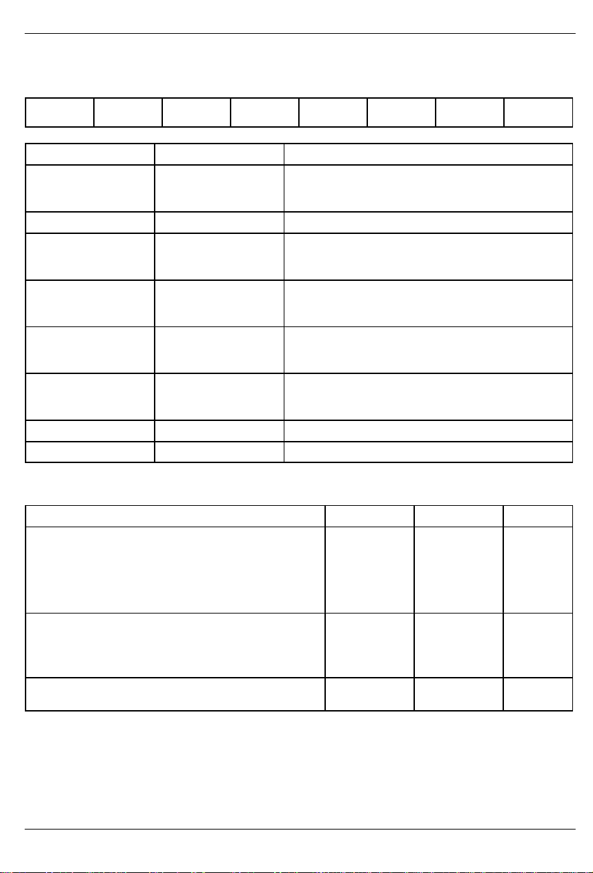
RECOMMENDED DC OPERATING CONDITIONS (0°C to 70°C)
PARAMETER SYMBOL MIN TYP MAX UNITS NOTES
Logic 1
Logic 0
Supply
V
IH
V
IL
V
CC
2.0 VCC+0.3 V
-0.3 +0.8 V
4.5 5.5 V
CAPACITANCE (t
= 25°C)
A
PARAMETER SYMBOL MIN TYP MAX UNITS NOTES
Input Capacitance C
Output Capacitance C
IN
OUT
DC ELECTRICAL CHARACTERISTICS (0°C to 70°C; V
5 pF
10 pF
= 5V + 10%)
CC
PARAMETER SYMBOL MIN TYP MAX UNITS NOTES
Active Supply Current I
Power-Down Current I
Input Leakage I
Output Leakage I
Output Current (2.4V) I
Output Current (0.4V) I
DDA
DDPD
ILK
OLK
OH
OL
-1.0 +1.0 µA
-1.0 +1.0 µA 4
-1.0 mA
+4.0 mA
20 mA 1,2
1 mA 1,2,3
NOTES:
1. PCMCLK= CPXCLK = 2.048 MHz; MCLK = 12 MHz.
2. Outputs open; inputs swinging full supply levels.
3. Control register bits CPD1= CPD2 = 1.
4. PCMOUT and CPXOUT are tri-stated.
041295 15/22
Page 16

DS2130Q
DTMF RECEIVER CHARACTERISTICS (0°C to 70°C; V
= +5V + 10%)
CC
PARAMETER SYMBOL MIN TYP MAX UNITS NOTES
Valid Detect Amplitude Range -40 0 dBm0 1,2
Frequency Deviation Accept +1.5 % 3
Frequency Deviation Reject +3.5 % 3
Minimum Twist Accept Range -10 +10 dB 4
Talk Off
5 Hits 5
(Mitel Test Tape #CM7291)
Noise Tolerance
-12 dB 6
(Mitel Test Tape #CM7291)
NOTES:
1. All DTMF receiver tests performed using test circuit shown in Figure 12.
2. Individual tone level of the DTMF pair.
3. Percent of nominal frequency for the individual tone.
4. Twist = 20 LOG (Hi tone/Lo tone).
5. Talk Off is a measure of the speech immunity of a DTMF receiver; the lower the number of hits, the better the
immunity .
6. Three KHz bandlimited white noise, referenced to lowest amplitude tone in the DTMF pair.
DTMF RECEIVER TIMING (0°C to 70°C; VCC = +5V + 10%)
PARAMETER SYMBOL MIN TYP MAX UNITS NOTES
Tone Duration Accept t
Tone Duration Reject t
Interdigit Pause Accept t
Interdigit Pause Reject t
Detect Delay (DT0-3) t
TAC
TRJ
PAC
PRJ
DTD
40 ms 1
20 ms
40 ms
20 ms
25 45 ms
NOTE:
1. See Figure 13 for DTMF receiver timing diagrams.
DTMF/TONE GENERATOR CHARACTERISTICS (0°C to 70°C; VCC = +5V + 10%)
PARAMETER SYMBOL MIN TYP MAX UNITS NOTES
DTMF Frequency Deviation
+1.0 % 1, 2
(each tone of the pair)
DTMF High Tone Level -6.0 dBm0
DTMF Low Tone Level -6.0 dBm0
Output Twist (DTMF only) 0.0 dB
1004 Hz Tone Level 0.0 dBm0
620, 350 Hz Tone Level -12.0 dBm0
Output Distortion (single tone) -25 dB 3
NOTES:
1. All tests performed using test circuit in Figure 12. Zero dBm0 = 1.231 Vrms with the Hitachi HD44238 codec/filter device.
2. PCMFS = CPXFS = 8.0 KHz +
3. Total harmonic distortion relative to test tone signal.
041295 16/22
0.1%.
Page 17

DS2130Q
DTMF RECEIVER/GENERATOR TEST CIRCUIT Figure 12
+5V
DTMF
INPUT
DTMF
OUTPUT
0 dBm0 = 1.231 Vrms
0.1 uF
10K
+5V
–5V
NC
CODEC/FILTER
GA2
PCMOUT
GA1
AIN
VREF
AOUT
PD
VDD
VSS
DGND
AGND
PCMIN
TXCLK
RXCLK
TXSYNC
RXSYNC
500
+5V
DS2130
PCMIN
PCMOUT
SPS
V
CC
GND
PCMCLK
CPXCLK
CPXFS
PCMFS
TM0
DT.0–DT.3
TM1
RST
CPXOUT
CPXIN
SDI
SCLK
MCLK
CS
NC
4
Power-on
Reset
Host
uProcessor
Detect
Monitor
CLK1
CLK2
CLK3
CLK1 = 11-13 MHz square wave
CLK2 = 2.048 MHz +
CLK3 = 8 KHz (must be derived from 2.048 source)
DTMF RECEIVER TIMING Figure 13
t
PAC
Energy reporting
DTMF
INPUT
DT0-3
t
TAC
DTMF
DIGIT 1
t
DTD
0001
0.1%
t
TRJ
DTMF
DIGIT 5
DTMF
DIGIT 9
t
PRJ
DTMF reporting
DTMF
DIGIT 9
1001
041295 17/22
Page 18

DS2130Q
PCM INTERFACE
AC ELECTRICAL CHARACTERISTICS (0°C to 70°C; V
PARAMETER SYMBOL MIN TYP MAX UNITS NOTES
PCMCLK, CPXCLK Clock Period t
PCMCLK, CPXCLK Pulse Width
High
PCMCLK, CPXCLK Rise, Fall
Times
Hold Time from PCMCLK,
t
CPXCLK to PCMFS, CPXFS
Setup Time from PCMFS, CPXFS
high to PCMCLK, CPXCLK low
Hold Time from PCMCLK,
CPXCLK Low to PCMFS, CPXFS
Low
Setup Time for PCMIN, CPXIN to
PCMCLK, CPXCLK Low
Hold Time for PCMIN, CPXIN to
PCMCLK, CPXCLK Low
Delay Time from PCMCLK,
CPXCLK to Valid PCMOUT,
CPXOUT
Delay Time from PCMCLK,
CPXCLK to PCMOUT, CPXOUT
3-stated
P
t
WH
t
R
t
F
HOLD
t
SF
t
HF
t
SD
t
HD
t
DO
t
DZ
244 5208 ns 1
100 ns
10 20 ns
0 ns 2
50 ns 2
100 ns 2
50 ns 2
50 ns 2
10 150 ns 3
20 150 ns 2,3,4
=5V + 10%)
CC
NOTES:
1. At least nine CPXCLK( or PCMCLK) clocks must be received within 1/3 of the CPXFS (or PCMFS) period.
2. Measured at V
3. Load = 150 pF + 2 LSTTL loads.
4. For LSB of PCM or CPX word.
041295 18/22
= 2.0V, VIL = 0.8V , and 10 ns maximum rise and fall times.
IH
Page 19

DS2130Q
MASTER CLOCK / RESET
AC ELECTRICAL CHARACTERISTICS (0°C to 70°C; V
PARAMETER SYMBOL MIN TYP MAX UNITS NOTES
MCLK Period t
MCLK Duty Cycle
/ t
+ t
(t
WMH
WML
WMH
)
MCLK Rise/Fall Times t
RST Pulse Width t
PM
RM
t
FM
RST
75 95 ns 1
45 55 %
10 ns
1 ms
=5V + 10%)
CC
NOTE:
1. MCLK = 10.5 to 12.5 MHz typically.
SERIAL PORT
AC ELECTRICAL CHARACTERISTICS (0°C to 70°C; V
PARAMETER SYMBOL MIN TYP MAX UNITS NOTES
SDI to SCLK Setup t
SCLK to SDI Hold t
SCLK Low Time t
SCLK High Time t
SCLK Rise and Fall Time
CS to SCLK Setup t
SCLK to CS Hold t
CS Inactive Time t
SCLK Setup to CS Falling t
DC
CDH
CL
CH
tR, t
CC
CCH
CWH
SCC
F
55 ns 1
55 ns 1
250 ns 1
250 ns 1
100 ns 1
50 ns 1
250 ns 1
250 ns 1
50 ns 1
= 5V + 10%)
CC
NOTE:
1. Measured at VIH = 2.0V, VIL = 0.8V , and 10 ns maximum rise and fall times.
041295 19/22
Page 20

DS2130Q
PCM INTERFACE AC TIMING DIAGRAM Figure 14
t
t
HF
t
SF
FR
t
HF
(MSB)
(MSB)
t
DO
CPXCLK
PCMCLK
CPXFS
PCMFS
CPXFS
PCMFS
CPXIN
PCMIN
CPXOUT
PCMOUT
tt
HOLD
3–STATE
MASTER CLOCK / RESET AC TIMING DIAGRAM Figure 15
tt
RM FM
MCLK
t
P
tt
WH WL
tt
SD
tt
HD
t
PM
WMH WML
t
DZ
t
RST
RST
SERIAL PORT AC TIMING DIAGRAM
CS
tt
t
CDH
t
DC
CC CH
t
SCC
SCLK
SDI
NOTE:
SCLK may be either high or low when CS is taken low.
041295 20/22
Figure 16
tt
RF
t
CL
t
CWH
t
CCH
Page 21

DS2130Q
DS2130 VOICE MESSAGING PROCESSOR 28-PIN DIP
28 15
B
1
13 EQUAL SPACES AT + .010
INCHES
DIM MIN MAX
A 1.240 1.280
B .540 .560
C .140 .160
D .590 .610
E .020 .040
F .110 .130
G .090 .110
H .600 .680
J .008 .012
K .015 .021
A
TNA
14
D
C
F
E
GK
J
H
041295 21/22
Page 22

DS2130Q VOICE MESSAGING PROCESSOR 28-PIN PLCC
E
E1
N
1
CH1
E2
INCHES
DIM MIN MAX
A 0.165 0.180
A1 0.090 0.120
A2 0.020 –
B 0.026 0.033
B1 0.013 0.021
C 0.009 0.012
D 0.485 0.495
D1 0.450 0.456
D2 0.390 0.430
E 0.485 0.495
E1 0.450 0.456
E2 0.390 0.430
L1 0.060 –
N 28 –
e1 0.050 BSC
CH1 0.042 0.048
D1 D D2
e1
DS2130Q
B
L1
B1
A
C
A1A2
041295 22/22
 Loading...