

Page 1

SPECIAL FEATURES
1993
DS1992/DS1993
www.dalsemi.com
§ 4096 bits of read/write nonvolatile memory
(DS1993 and DS1994)
§ 1024 bits of read/write nonvolatile memory
(DS1992)
§ 256-bit scratchpad ensures integrity of data
transfer
§ Memory partitioned into 256-bit pages for
packetizing data
§ Data integrity assured with strict read/write
protocols
§ Contains real time clock/calendar in binary
format (DS1994)
§ Interval timer can automatically accumulate
time when power is applied (DS1994)
§ Programmable cycle counter can accumulate
the number of system power-on/off cycles
(DS1994)
§ Programmable alarms can be set to generate
interrupts for interval timer, real time clock,
and/or cycle counter (DS1994)
§ Write protect feature provides tamper-proof
time data (DS1994)
§ Programmable expiration date that will limit
access to SRAM and timekeeping (DS1994)
§ Clock accuracy is better than ±2 minute/
month at 25°C (DS1994)
§ Operating temperature range from -40°C to
+70°C
§ Over 10 years of data retention
1kbit/4kbit Memory iButton
DS1994
4-kbit Plus Time Memory iButton
§ Data can be accessed while affixed to object
§ Economically communicates to bus master
with a single digital signal at 16.3k bits per
second
§ Standard 16 mm diameter and 1-Wire
protocol ensure compatibility with iButton
family
§ Button shape is self-aligning with cup-
shaped probes
§ Durable stainless steel case engraved with
registration number withstands harsh
environments
§ Easily affixed with self-stick adhesive
backing, latched by its flange, or locked with
a ring pressed onto its rim
§ Presence detector acknowledges when reader
first applies voltage
§ Meets UL#913 (4th Edit.); Intrinsically Safe
Apparatus, Approved under Entity Concept
for use in Class I, Division 1, Group A, B, C
and D Locations
F5 MICROCAN
5.89
0.36
TM
0.51
YYWW REGISTERED RR
AF
000000FBC52B
c
04
16.25
17.35
TM
TM
COMMON iButton FEATURES
§ Unique, factory-lasered and tested 64-bit
registration number (8-bit family code + 48bit serial number + 8-bit CRC tester) assures
absolute traceability because no two parts are
alike
§ Multidrop controller for MicroLAN
§ Digital identification and information by
momentary contact
§ Chip–based data carrier compactly stores
information
DATA
GROUND
All diminsions shown in millimeters.
ORDERING INFORMATION
DS1992L-F5 F5 MicroCan
DS1993L-F5 F5 MicroCan
DS1994L-F5 F5 MicroCan
1 of 23 102199
Page 2

DS1992/DS1993/DS1994
EXAMPLES OF ACCESSORIES
DS9096P Self-Stick Adhesive Pad
DS9101 Multi-Purpose Clip
DS9093RA Mounting Lock Ring
DS9093F Snap-In Fob
DS9092 iButton Probe
iButton DESCRIPTION
The DS1992/DS1993/DS1994 Memory iButton (hereafter referred to as DS199X) is a rugged read/write
data carrier that acts as a localized database that can be easily accessed with minimal hardware. The
nonvolatile memory and optional timekeeping capability offer a simple solution to storing and retrieving
vital information pertaining to the object to which the iButton is attached. Data is transferred serially via
the 1–Wire protocol which requires only a single data lead and a ground return.
The scratchpad is an additional page that acts as a buffer when writing to memory. Data is first written to
the scratchpad where it can be read back. After the data has been verified, a copy scratchpad command
will transfer the data to memory. This process ensures data integrity when modifying the memory. A 48–
bit serial number is factory lasered into each DS199X to provide a guaranteed unique identity which
allows for absolute traceability. The durable MicroCan package is highly resistant to environmental
hazards such as dirt, moisture, and shock. Its compact coin–shaped profile is self–aligning with mating
receptacles, allowing the DS199X to be easily used by human operators. Accessories permit the DS199X
to be mounted on almost any surface including plastic key fobs, photo–ID badges and printed circuit
boards.
Applications include access control, work–in–progress tracking, electronic travelers, storage of
calibration constants, and debit tokens. With the optional time-keeping functions (DS1994), a real time
clock/calendar, interval timer, cycle counter, and programmable interrupts are available in addition to the
nonvolatile memory. The internal clock can be programmed to deny memory access based on absolute
time/date, total elapsed time, or the number of accesses. These features allow the DS1994 to be used to
create a stopwatch, alarm clock, time and date stamp, logbook, hour meter, calendar, system power cycle
timer, interval timer, and event scheduler.
OPERATION
The DS199X has four main data components: 1) 64-bit lasered ROM, 2) 256-bit scratchpad, 3) 1024–bit
(DS1992) or 4096–bit (DS1993 and DS1994) SRAM, and 4) timekeeping registers (DS1994). The
timekeeping section utilizes an on-chip oscillator that is connected to a 32.768 kHz crystal. The SRAM
and time-keeping registers reside in one contiguous address space referred to hereafter as memory. All
data is read and written least significant bit first.
The memory functions will not be available until the ROM function protocol has been established. This
protocol is described in the ROM functions flow chart (Figure 9). The master must first provide one of
four ROM function commands: 1) read ROM, 2) match ROM, 3) search ROM, or 4) skip ROM. After a
ROM function sequence has been successfully executed, the memory functions are accessible and the
master may then provide any one of the four memory function commands (Figure 6).
2 of 23 102199
Page 3
DS1992/DS1993/DS1994
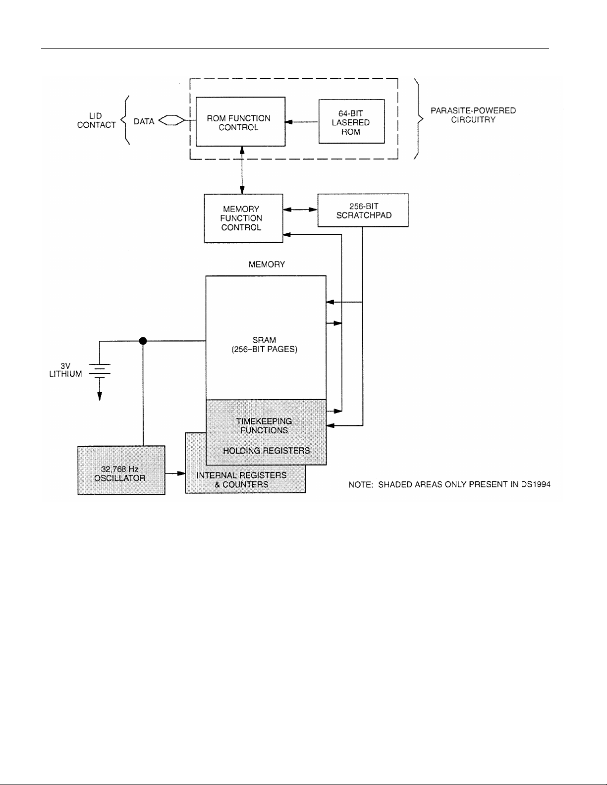
DS199X BLOCK DIAGRAM Figure 1
3 of 23 102199
Page 4
DS1992/DS1993/DS1994
PARASITE POWER
The block diagram (Figure 1) shows the parasite-powered circuitry. This circuitry “steals” power
whenever the data input is high. The data line will provide sufficient power as long as the specified
timing and voltage requirements are met. The advantages of parasite power are two-fold: 1) by parasiting
off this input, lithium is conserved and 2) if the lithium is exhausted for any reason, the ROM may still be
read normally.
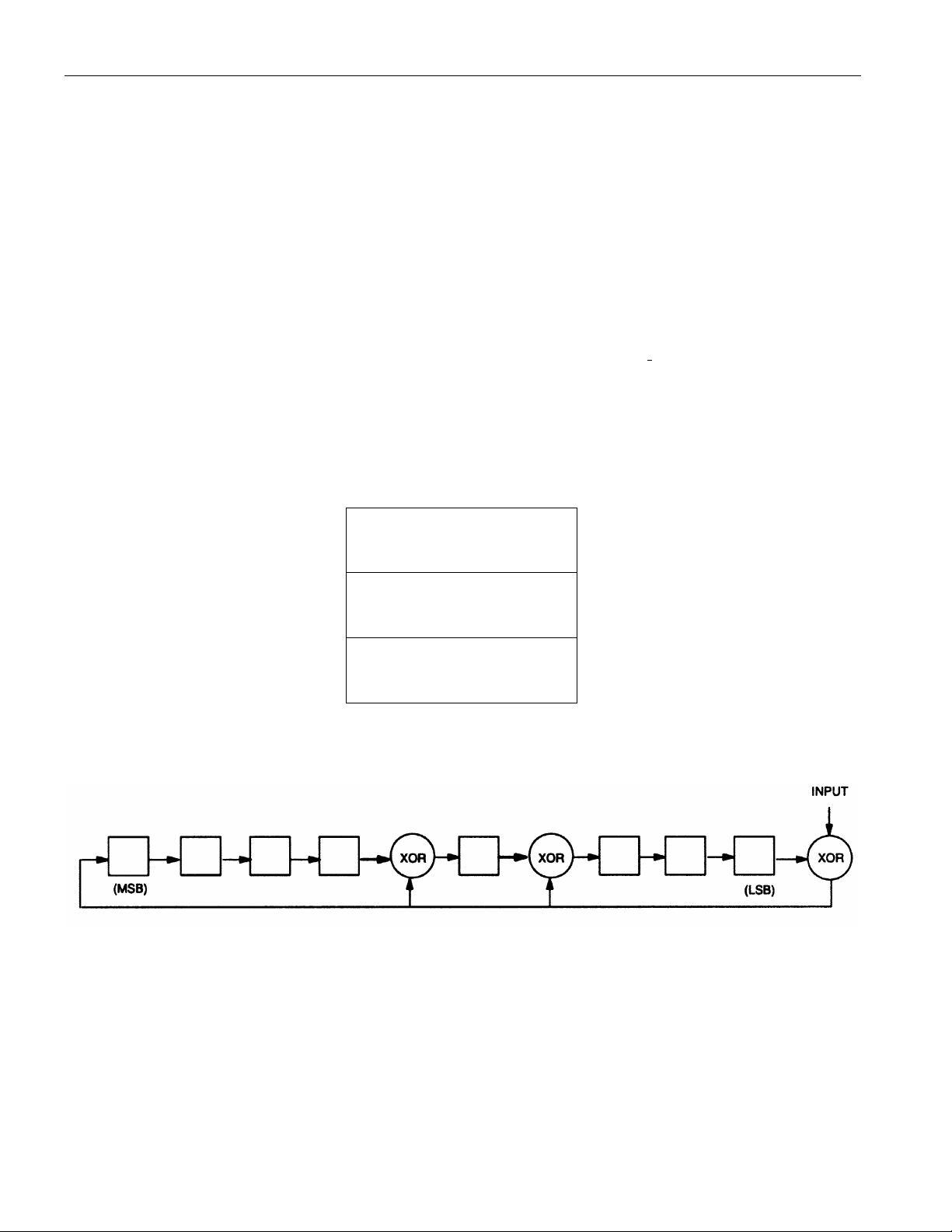
64-BIT LASERED ROM
Each DS199X contains a unique ROM code that is 64 bits long. The first eight bits are a 1-Wire family
code. The next 48 bits are a unique serial number. The last eight bits are a CRC of the first 56 bits. (See
Figure 2.) The 1-wire CRC is generated using a polynomial generator consisting of a shift register and
XOR gates as shown in Figure 3. The polynomial is X
8
+ X5 + X4 + 1. Additional information about the
Dallas 1-Wire Cyclic Redundancy Check is available in the Book of DS19xx iButton Standards. The shift
register bits are initialized to zero. Then starting with the least significant bit of the family code, one bit at
a time is shifted in. After the 8th bit of the family code has been entered, then the serial number is
entered. After the 48th bit of the serial number has been entered, the shift register contains the CRC
value. Shifting in the eight bits of CRC should return the shift register to all zeros.
64-BIT LASERED ROM Figure 2
FAMILY
CODE
SERIAL
NUMBER
CRC 8 BITS
1-WIRE CRC CODE Figure 3
04h = DS1994
06h = DS1993
08h = DS1992
48-BIT
UNIQUE
NUMBER
LSB
MSB
4 of 23 102199
Page 5
DS1992/DS1993/DS1994
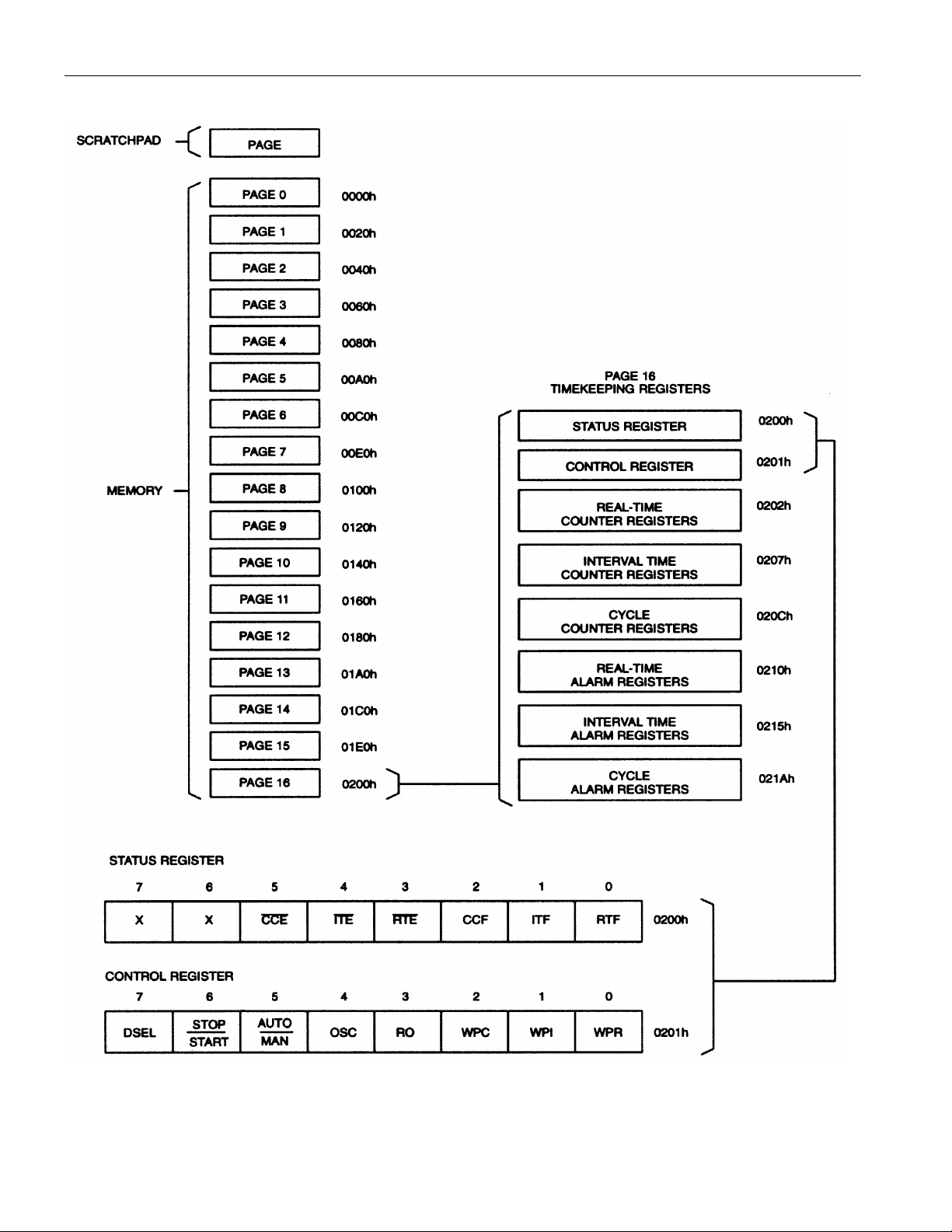
DS1994 MEMORY MAP Figure 4a
5 of 23 102199
Page 6
DS1992/DS1993/DS1994
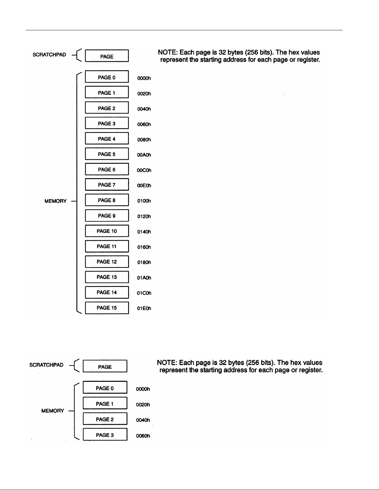
DS1993 MEMORY MAP Figure 4b
DS1992 MEMORY MAP Figure 4c
6 of 23 102199
Page 7

DS1992/DS1993/DS1994
MEMORY
The memory map in Figure 4 shows a 32–byte page called the scratchpad and additional 32–byte pages
called memory. The DS1992 contains pages 0 though 3 which make up the 1024–bit SRAM. The
DS1993 and DS1994 contain pages 0 through 15 which make up the 4096–bit SRAM. The DS1994 also
contains page 16 which has only 30 bytes that contain the timekeeping registers.
The scratchpad is an additional page that acts as a buffer when writing to memory. Data is first written to
the scratchpad where it can be read back. After the data has been verified, a copy scratchpad command
will transfer the data to memory. This process ensures data integrity when modifying the memory.
TIMEKEEPING (DS1994)
A 32.768 kHz crystal oscillator is used as the time base for the timekeeping functions. The oscillator can
be turned on or off by an enable bit in the control register. The oscillator must be on for the real time
clock, interval timer and cycle counter to function.
The timekeeping functions are double buffered. This feature allows the master to read time or count
without the data changing while it is being read. To accomplish this, a snapshot of the counter data is
transferred to holding registers which the user accesses. This occurs after the eighth bit of the Read
Memory Function command.
Real-Time Clock
The real-time clock is a 5-byte binary counter. It is incremented 256 times per second. The least
significant byte is a count of fractional seconds. The upper four bytes are a count of seconds. The realtime clock can accumulate 136 years of seconds before rolling over. Time/date is represented by the
number of seconds since a reference point which is determined by the user. For example, 12:00 A.M.,
January 1, 1970 could be a reference point.
Interval Timer
The interval timer is a 5-byte binary counter. When enabled, it is incremented 256 times per second. The
least significant byte is a count of fractional seconds. The interval timer can accumulate 136 years of
seconds before rolling over. The interval timer has two modes of operation which are selected by the
AUTO/MAN bit in the control register. In the auto mode, the interval timer will begin counting after the
data line has been high for a period of time determined by the DSEL bit in the control register. Similarly,
the interval timer will stop counting after the data line has been low for a period of time determined by
the DSEL bit. In the manual mode, time accumulation is controlled by the STOP/START bit in the
control register.
NOTE: For auto mode operation, the high level on the data line must be greater than or equal to 2.1 volts.
Cycle Counter
The cycle counter is a 4-byte binary counter. It increments after the falling edge of the data line if the
appropriate data line timing has been met. This timing is selected by the DSEL bit in the control register.
(See “Status/Control” section).
NOTE: For cycle counter operation, the high level on the data line must be greater than or equal to 2.1
volts.
7 of 23 102199
Page 8

DS1992/DS1993/DS1994
Alarm Registers
The alarm registers for the real-time clock, interval timer, and cycle counter all operate in the same
manner. When the value of a given counter equals the value in its associated alarm register, the
appropriate flag bit is set in the status register. If the corresponding interrupt enable bit(s) in the status
register is set, an interrupt is generated. If a counter and its associated alarm register are write protected
when an alarm occurs, access to the device becomes limited. (See “Status/Control”, “Interrupts”, and the
“Programmable Expiration” sections.)
STATUS/CONTROL REGISTERS (DS1994)
The status and control registers are the first two bytes of page 16 (see “Memory Map”, Figure 4).
Status Register
7 6 5 4 3 2 1 0
X X CCE ITE RTE CCF ITF RTF 0200h
Don’t care bits Read Only
0 RTF Real-time clock alarm flag
1 ITF Interval timer alarm flag
2 CCF Cycle counter alarm flag
When a given alarm occurs, the corresponding alarm flag is set to a logic 1. The alarm flag(s) is cleared
by reading the status register.
3 RTE Real-time clock alarm flag
4 ITE Interval timer alarm flag
5 CCE Cycle counter alarm flag
Writing any of the interrupt enable bits to a logic 0 will allow an interrupt condition to be generated when
its corresponding alarm flag is set (see “Interrupts” section).
8 of 23 102199
Page 9

DS1992/DS1993/DS1994
Control Register
7 6 5 4 3 2 1 0
DSEL
0 WPR Write protect real-time clock/alarms registers
1 WPI Write protect interval timer/alarms registers
2 WPC Write protect cycle counter/alarms registers
Setting a write protect bit to a logic 1 will permanently write protect the corresponding counter and alarm
registers, all write protect bits, and additional bits in the control register. The write protect bits can not be
written in a normal manner (see “Write Protect/Programmable Expiration” section).
3 RO Read only
If a programmable expiration occurs and the read only bit is set to a logic 1, then the DS1994 becomes
read only. If a programmable expiration occurs and the read only bit is a logic 0, then only the 64-bit
lasered ROM can be accessed (see “Write Protect/Programmable Expiration” section).
STOP
START
AUTO
MAN.
OSC RO WPC WPI WPR 0201h
4 OSC Oscillator enable
This bit controls the crystal oscillator. When set to a logic 1, the oscillator will start operation. When the
oscillator bit is a logic 0, the oscillator will stop.
5 AUTO/MAN Automatic/Manual Mode
When this bit is set to a logic 1, the interval timer is in automatic mode. In this mode, the interval timer is
enabled by the data line. When this bit is set to a logic 0, the interval timer is in manual mode. In this
mode the interval timer is enabled by the STOP/START bit.
6 STOP/START Stop/Start (in Manual Mode)
If the interval timer is in manual mode, the interval timer will start counting when this bit is set to a logic
0 and will stop counting when set to a logic 1. If the interval timer is in automatic mode, this bit has no
effect.
7 DSEL Delay Select Bit
This bit selects the delay that it takes for the cycle counter and the interval timer (in auto mode) to see a
transition on the data line. When this bit is set to a logic 1, the delay time is 123 ± 2 ms. This delay allows
communication on the data line without starting or stopping the interval timer and without incrementing
the cycle counter. When this bit is set to a logic 0, the delay time is 3.5 ± 0.5 ms.
9 of 23 102199
Page 10

DS1992/DS1993/DS1994
MEMORY FUNCTION COMMANDS
The “Memory Function Flow Chart” (Figure 6) describes the protocols necessary for accessing the
memory. An example follows the flowchart. Three address registers are provided as shown in Figure 5.
The first two registers represent a 16-bit target address (TA1, TA2). The third register is the ending
offset/data status byte (E/S).
The target address points to a unique byte location in memory. The first five bits of the target address
(T4:T0) represent the byte offset within a page. This byte offset points to one of 32 possible byte
locations within a given page. For instance, 00000b points to the first byte of a page where as 11111b
would point to the last byte of a page.
The third register (E/S) is a read only register. The first five bits (E4: E0) of this register are called the
ending offset. The ending offset is a byte offset within a page (1 of 32 bytes). Bit 5 (PF) is the partial byte
flag. Bit 6 (OF) is the overflow flag. Bit 7 (AA) is the authorization accepted flag.
ADDRESS REGISTERS Figure 5
7 6 5 4 3 2 1 0
TARGET ADDRESS (TA1) T7 T6 T5 T4 T3 T2 T1 T0
TARGET ADDRESS (TA2) T15 T14 T13 T12 T11 T10 T9 T8
ENDING ADDRESS WITH
DATA STATUS (E/S)
(READ ONLY)
AA OF PF E4 E3 E2 E1 E0
Write Scratchpad Command [0Fh]
After issuing the write scratchpad command, the user must first provide the 2-byte target address,
followed by the data to be written to the scratchpad. The data will be written to the scratchpad starting at
the byte offset (T4:T0). The ending offset (E4: E0) will be the byte offset at which the host stops writing
data. The maximum ending offset is 11111b (31d). If the host attempts to write data past this maximum
offset, the overflow flag (OF) will be set and the remaining data will be ignored. If the user writes an
incomplete byte and an overflow has not occurred, the partial byte flag (PF) will be set.
Read Scratchpad Command [AAh]
This command may be used to verify scratchpad data and target address. After issuing the read scratchpad
command, the user may begin reading. The first two bytes will be the target address. The next byte will
be the ending offset/data status byte (E/S) followed by the scratchpad data beginning at the byte offset
(T4: T0). The user may read data until the end of the scratchpad after which the data read will be all logic
1’s.
10 of 23 102199
Page 11

DS1992/DS1993/DS1994
Copy Scratchpad [55h]
This command is used to copy data from the scratchpad to memory. After issuing the copy scratchpad
command, the user must provide a 3-byte authorization pattern. This pattern must exactly match the data
contained in the three address registers (TA1, TA2, E/S, in that order). If the pattern matches, the AA
(Authorization Accepted) flag will be set and the copy will begin. A logic 0 will be transmitted after the
data has been copied until a reset pulse is issued by the user. Any attempt to reset the part will be ignored
while the copy is in progress. Copy typically takes 30 µs.
The data to be copied is determined by the three address registers. The scratchpad data from the
beginning offset through the ending offset, will be copied to memory, starting at the target address.
Anywhere from 1 to 32 bytes may be copied to memory with this command. Whole bytes are copied even
if only partially written. The AA flag will be cleared only by executing a write scratchpad command.
Read Memory [F0h]
The read memory command may be used to read the entire memory. After issuing the command, the user
must provide the 2-byte target address. After the two bytes, the user reads data beginning from the target
address and may continue until the end of memory, at which point logic 1’s will be read. It is important to
realize that the target address registers will contain the address provided. The ending offset/data status
byte is unaffected.
The hardware of the DS1992/DS1993/DS1994 provides a means to accomplish error–free writing to the
memory section. To safeguard reading data in the 1–Wire environment and to simultaneously speed up
data transfers, it is recommended to packetize data into data packets of the size of one memory page each.
Such a packet would typically store a 16–bit CRC with each page of data to ensure rapid, error–free data
transfers that eliminate having to read a page multiple times to determine if the received data is correct or
not. (See the Book of DS19xx iButton Standards, Chapter 7 for the recommended file structure to be used
with the 1–Wire environment.)
11 of 23 102199
Page 12

DS1992/DS1993/DS1994
MEMORY FUNCTIONS FLOW CHART Figure 6
12 of 23 102199
Page 13

DS1992/DS1993/DS1994
TX
00h
MEMORY FUNCTION EXAMPLES
Example: Write two data bytes to memory locations 0026h and 0027h (the seventh and eighth bytes of
page 1). Read entire memory.
MASTER MODE DATA (LSB FIRST) COMMENTS
TX Reset
RX Presence Presence pulse
TX CCh Issue “skip ROM” command
TX 0Fh Issue “write scratchpad command
TX 26h TA1, beginning offset = 6
TX 00h TA2, address = 0026h
TX <2 data bytes> Write 2 bytes of data to scratchpad
TX Reset Reset pulse
RX Presence Presence pulse
TX CCh Issue “skip ROM” command
TX AAh Issue “read scratchpad command
RX 26h Read TA1, beginning offset = 6
RX 00h Read TA2, address = 0026h
RX 07h Read E/S, ending offset = 7, flags = 0
RX <2 data bytes> Read scratchpad data and verify
TX Reset Reset pulse
RX Presence Presence pulse
TX CCh Issue “skip ROM” command
TX 55h Issue “copy scratchpad command
TX 26h
TX 07h
TX Reset Reset pulse
RX Presence Presence pulse
TX CCh Issue “skip ROM” command
TX F0h Issue “read memory command
TX 00h TA1, beginning offset = 6
TX 00h TA2, address = 0000h
RX <128 bytes (DS1992)>
<512 bytes (DS1993)>
<542 bytes (DS1994)>
TX Reset Reset pulse
RX Presence Presence pulse, done
Reset pulse (480-960 µs)
TA1
TA2 AUTHORIZATION CODE
E/S
Read entire memory
13 of 23 102199
Page 14

DS1992/DS1993/DS1994
WRITE PROTECT/PROGRAMMABLE EXPIRATION (DS1994)
The write protect bits (WPR, WPI, WPC) provide a means of write protecting the timekeeping data and
limiting access to the DS1994 when an alarm occurs (programmable expiration). The write protect bits
may not be written by performing a single copy scratchpad command. Instead, to write these bits, the
copy scratchpad command must be performed three times. Please note that the AA bit will set, as
expected, after the first copy command is successfully executed. Therefore, the authorization pattern for
the second and third copy command should have this bit set. The read scratchpad command may be used
to verify the authorization pattern.
The write protect bits, once set, permanently write protect their corresponding counter and alarm
registers, all write protect bits, and certain control register bits as shown in Figure 7. The time/count
registers will continue to count if the oscillator is enabled. If the user wishes to set more than one write
protect bit, the user must set them at the same time. Once a write protect bit is set it cannot be undone,
and the remaining write protect bits, if not set, cannot be set. The programmable expiration takes place
when one or more write protect bits have been set and a corresponding alarm occurs. If the RO (read
only) bit is set, only the read scratch and read memory function commands are available. If the RO bit is a
logic “0”, no memory function commands are available. The ROM functions are always available.
WRITE PROTECT CHART Figure 7
WRITE PROTECT BIT SET: WPR WPI WPC
Data Protected from
User Modification:
* Becomes write “1” only, i.e., once written to a logic “1”, may not be written back to a logic “0”.
** Forced to a logic “0”.
Real Time Clock
Real Time Alarm
WPR
WPI
WPC
RO
OSC*
Interval Timer
Interval Time Alarm
WPR
WPI
WPC
RO
OSC*
STOP/START **
AUTO/MAN
Cycle Counter
Cycle Counter Alarm
WPR
WPI
WPC
RO
OSC*
DSEL
1-WIRE BUS SYSTEM
The 1-wire bus is a system which has a single bus master and one or more slaves. In most instances the
DS199X behaves as a slave. The exception is when the DS1994 generates an interrupt due to a
timekeeping alarm. The discussion of this bus system is broken down into three topics: hardware
configuration, transaction sequence, and 1-wire signaling (signal types and timing).
HARDWARE CONFIGURATION
The 1-wire bus has only a single line by definition; it is important that each device on the bus be able to
drive it at the appropriate time. To facilitate this, each device attached to the 1-wire bus must have open
drain or 3–state outputs. The 1-wire port of the DS199X is open drain with an internal circuit equivalent
to that shown in Figure 8. A multidrop bus consists of a 1–Wire bus with multiple slaves attached. The 1wire bus has a maximum data rate of 16.3k bits per second and requires a pull-up resistor of
approximately 5 kΩ. The idle state for the 1-wire bus is high. If for any reason a transaction needs to be
suspended, the bus MUST be left in the idle state if the transaction is to resume. If this does not occur and
the bus is left low for more than 120 µs, one or more of the devices on the bus may be reset.
14 of 23 102199
Page 15

DS1992/DS1993/DS1994
HARDWARE CONFIGURATION Figure 8
TRANSACTION SEQUENCE
The protocol for accessing the DS199X via the 1-wire port is as follows:
§ Initialization
§ ROM Function Command
§ Memory Function Command
§ Transaction/Data
INITIALIZATION
All transactions on the 1-wire bus begin with an initialization sequence. The initialization sequence
consists of a reset pulse transmitted by the bus master followed by presence pulse(s) transmitted by the
slave(s). The presence pulse lets the bus master know that the DS199X is on the bus and is ready to
operate. For more details, see the “1-Wire Signaling” section.
ROM FUNCTION COMMANDS
Once the bus master has detected a presence, it can issue one of the four ROM function commands. All
ROM function commands are eight bits long. A list of these commands follows (refer to flowchart in
Figure 9):
Read ROM [33h]
This command allows the bus master to read the DS199X’s 8-bit family code, unique 48-bit serial number, and 8-bit CRC. This command can only be used if there is a single DS199X on the bus. If more than
one slave is present on the bus, a data collision will occur when all slaves try to transmit at the same time
(open drain will produce a wired-AND result). The resultant family code and 48–bit serial number will
usually result in a mismatch of the CRC.
Match ROM [55h]
The match ROM command, followed by a 64-bit ROM sequence, allows the bus master to address a
specific DS199X on a multidrop bus. Only the DS199X that exactly matches the 64-bit ROM sequence
will respond to the subsequent memory function command. All slaves that do not match the 64-bit ROM
sequence will wait for a reset pulse. This command can be used with a single or multiple devices on the
bus.
15 of 23 102199
Page 16

DS1992/DS1993/DS1994
ROM FUNCTIONS FLOW CHART Figure 9
16 of 23 102199
Page 17

DS1992/DS1993/DS1994
Skip ROM [CCh]
This command can save time in a single drop bus system by allowing the bus master to access the
memory functions without providing the 64-bit ROM code. If more than one slave is present on the bus
and a read command is issued following the Skip ROM command, data collision will occur on the bus as
multiple slaves transmit simultaneously (open drain pull-downs will produce a wired-AND result).
Search ROM [F0h]
When a system is initially brought up, the bus master might not know the number of devices on the 1–
Wire bus or their 64–bit ROM codes. The search ROM command allows the bus master to use a process
of elimination to identify the 64–bit ROM codes of all slave devices on the bus. The search ROM process
is the repetition of a simple 3–step routine: read a bit, read the complement of the bit, then write the
desired value of that bit. The bus master performs this simple, 3–step routine on each bit of the ROM.
After one complete pass, the bus master knows the contents of the ROM in one device. The remaining
number of devices and their ROM codes may be identified by additional passes. See Chapter 5 of the
Book of DS19xx iButton Standards for a comprehensive discussion of a search ROM, including an actual
example.
Search Interrupt [ECh] (DS1994)
This ROM command works exactly as the normal ROM Search, but it will identify only devices with
interrupts that have not yet been acknowledged.
1–WIRE SIGNALING
The DS199x requires strict protocols to ensure data integrity. The protocol consists of five types of
signaling on one line: Reset Sequence with Reset Pulse and Presence Pulse, Write 0, Write 1, Read Data
and interrupt pulse (DS1994). All these signals except presence pulse and interrupt pulse are initiated by
the bus master. The initialization sequence required to begin any communication with the DS199x is
shown in Figure 10. A reset pulse followed by a presence pulse indicates the DS199x is ready to send or
receive data given the correct ROM command and memory function command. The bus master transmits
(TX) a reset pulse (t
, minimum 480 µs). The bus master then releases the line and goes into receive
RSTL
mode (RX). The 1–Wire bus is pulled to a high state via the pull–up resistor. After detecting the rising
edge on the data line, the DS199x waits (t
, 15–60 µs) and then transmits the presence pulse (t
PDH
PDL
, 60–
240 µs). There are special conditions if interrupts are enabled where the bus master must check the state
of the 1–Wire bus after being in the RX mode for 480 µs. These conditions will be discussed in the
“Interrupt” section.
READ/WRITE TIME SLOTS
The definitions of write and read time slots are illustrated in Figure 11. All time slots are initiated by the
master driving the data line low. The falling edge of the data line synchronizes the DS199x to the master
by triggering a delay circuit in the DS199x. During write time slots, the delay circuit determines when the
DS199x will sample the data line. For a read data time slot, if a “0” is to be transmitted, the delay circuit
determines how long the DS199x will hold the data line low overriding the 1 generated by the master. If
the data bit is a “1”, the iButton will leave the read data time slot unchanged.
17 of 23 102199
Page 18

DS1992/DS1993/DS1994
RESISTOR
INITIALIZATION PROCEDURE “RESET AND PRESENCE PULSES” Figure 10
MASTER
DS199x
480µs ≤ t
480µs ≤ t
15µs ≤ t
60µs ≤ t
< ∞ *
RSTL
< ∞ (includes recovery time)
RSTH
< 60 µs
PDH
< 240 µs
PDL
* In order not to mask interrupt signaling by other devices on the 1-Wire bus, t
less than 960 µs.
READ/WRITE TIMING DIAGRAM Figure 11
Write-One Time Slot
+ tR should always be
RSTL
60 µs ≤ t
1µs ≤ t
1µs ≤ t
LOW1
REC
< 120 µs
SLOT
< 15 µs
< ∞
18 of 23 102199
Page 19

DS1992/DS1993/DS1994
RESISTOR
READ/WRITE TIMING DIAGRAM Figure 11 (continued)
Write-Zero Time Slot
Read-Data Time Slot
MASTER
DS199x
60 µs ≤ t
1µs ≤ t
REC
60 µs ≤ t
1µs ≤ t
0 ≤ t
1µs ≤ t
t
RDV
LOWR
RELEASE
REC
= 15 µs
tSU < 1 µs
LOW0
< ∞
SLOT
< 15 µs
< ∞
< t
SLOT
< 120 µs
< 15 µs
120 µs
Interrupts (DS1994)
If the DS1994 detects an alarm condition, it will automatically set the corresponding alarm flag in the
Status Register. An interrupt condition begins whenever any alarm flag is set and the flag’s corresponding
interrupt bit is enabled. The interrupt condition ceases when the alarm flags are cleared (i.e., the interrupt
is acknowledged by reading the Status Register, address 200H) or if the corresponding interrupt enable bit
is disabled.
The DS1994 can produce two types of interrupts: spontaneous interrupts, called type 1, and delayed
interrupts, type 2. Spontaneous interrupts need to be armed by a Reset Pulse after all communication on
the 1–Wire bus has finished. A single falling slope on the 1–Wire bus will disarm this type of interrupt. If
an alarm condition occurs while the device is disarmed, at first a type 2 interrupt will be produced.
19 of 23 102199
Page 20

DS1992/DS1993/DS1994
Spontaneous interrupts are signaled by the DS1994 by pulling the data line low for 960 to 3840 µs as the
interrupt condition begins (Figure 12). After this long low pulse a Presence Pulse will follow. If the alarm
condition occurs just after the master has sent a Reset Pulse, i.e., during the high or low time of the
Presence Pulse, the DS1994 will not assert its Interrupt Pulse until the Presence Pulse is finished (Figure
13).
If the DS1994 cannot assert a spontaneous interrupt, either because the data line was not pulled high,
communication was in progress, or the interrupt was not armed, it will extend the next Reset Pulse to a
total length of 960 to 3840 µs (delayed interrupt). If the alarm condition occurs during the reset low time
of the Reset Pulse, the DS1994 will immediately assert its interrupt pulse; thus the total low time of the
pulse can be extended up to 4800 µs (Figure 14). If a DS1994 with a not previously signaled alarm
detects a power–on cycle on the 1–Wire bus, it will send a Presence Pulse and wait for the Reset Pulse
sent by the master to extend it and to subsequently issue a Presence Pulse (Figure 15). As long as an
interrupt has not been acknowledged by the master, the DS1994 will continue sending interrupt pulses.
The interrupt signaling discussed so far is valid for the first opportunity the device has to signal an
interrupt. It is not required for the master to acknowledge an interrupt immediately. If an interrupt is not
acknowledged, the DS1994 will continue signaling the interrupt with every Reset Pulse. To do so,
DS1994 devices of Revision B (earlier production parts) will always use the waveform of the Type 2
Interrupt (Figure 14). Devices of Revision C (latest production) will either use the waveform of the Type
2 Interrupt (Figure 14) or the waveform of the Type 1A Interrupt (Figure 13). The waveform of the Type
2 Interrupt will be observed after a communication to a device other than the interrupting one; after
successful communication to the interrupting device (without acknowledging the interrupt) the waveform
of the Type 1A Interrupt will be found.
The revision code of the DS1994 is branded on the lid of the MicroCan. The field RR (see figure on Page
1), just a above the family code, will read Bx for Revision B and Cx for Revision C. (The character “x”
represents a 1-digit number that is not related to the chip inside.) The revision code can also be
determined indirectly by observing the waveforms used for interrupt signaling.
TYPE 1 INTERRUPT Figure 12
20 of 23 102199
Page 21

DS1992/DS1993/DS1994
TYPE 1A INTERRUPT (SPECIAL CASE) Figure13
TYPE 2 INTERRUPT Figure14
TYPE 2 INTERRUPT (SPECIAL CASE) Figure15
21 of 23 102199
Page 22

DS1992/DS1993/DS1994
PHYSICAL SPECIFICATIONS
Size See mechanical drawing
Weight 3.3 grams (F5 package)
Humidity 90% RH at 50°C
Altitude 10,000 feet
Expected Service Life 10 years at 25°C
Safety Meets UL#913 (4th Edit.); Intrinsically Safe Apparatus,
Approved under Entity Concept for use in Class I,
Division 1, Group A, B, C and D Locations
ABSOLUTE MAXIMUM RATINGS*
Voltage on any Pin Relative to Ground –0.5V to +7.0V
Operating Temperature –40°C to +70°C
Storage Temperature –40°C to +70°C
* This is a stress rating only and functional operation of the device at these or any other conditions above
those indicated in the operation sections of this specification is not implied. Exposure to absolute maximum rating conditions for extended periods of time may affect reliability.
DC ELECTRICAL CHARACTERISTICS (V
=2.8V to 6.0V; -40°C to +70°C)
PUP
PARAMETER SYMBOL MIN TYP MAX UNITS NOTES
Logic 1 V
Logic 0 V
Output Logic Low @ 4 mA V
Output Logic High V
Input Load Current
IH
IL
OL
OH
I
L
2.2 VCC +0.3 V 1,8
-0.3 +0.8 V 1
0.4 V 1
V
PUP
5
6.0 V 1,2
µA
3
CAPACITANCE (tA = 25°C)
PARAMETER SYMBOL MIN TYP MAX UNITS NOTES
I/O (1-Wire) C
IN/OUT
AC ELECTRICAL CHARACTERISTICS (V
PARAMETER SYMBOL MIN TYP MAX UNITS NOTES
Time Slot
Write 1 Low Time
Write 0 Low Time
Read Data Valid
Release Time
Read Data Setup
Interrupt
Recovery Time
Reset Time High
Reset Time Low
Presence Detect High
Presence Detect Low
t
SLOT
t
LOW1
t
LOW0
t
RDV
t
RELEASE
t
SU
t
INT
t
REC
t
RSTH
t
RSTL
t
PDH
t
PDL
60 120
1 15
60 120
0 15 45
960 4800
1
480
480 960
15 60
60 240
100 800 pF 6
=2.8V to 6.0V; -40°C to +70°C)
PUP
µs
µs
µs
exactly 15
µs
µs
1
µs
µs
µs
µs
µs
µs
µs
5
9
4
7
22 of 23 102199
Page 23

DS1992/DS1993/DS1994
NOTES:
1. All voltages are referenced to ground.
2. V
= external pull–up voltage.
PUP
3. Input load is to ground.
4. An additional reset or communication sequence cannot begin until the reset high time has expired.
5. Read data setup time refers to the time the host must pull the 1–Wire bus low to read a bit. Data is
guaranteed to be valid within 1 µs of this falling edge and will remain valid for 14 µs minimum. (15
µs total from falling edge on 1–Wire bus.)
6. Capacitance on the data line could be 800 pF when power is first applied. If a 5 kΩ resistor is used to
pull–up the data line to VCC, 5 µs after power has been applied, the parasite capacitance will not affect
normal communications.
7. The reset low time (t
) should be restricted to a maximum of 960 µs, to allow interrupt signaling,
RSTL
otherwise, it could mask or conceal interrupt pulses.
8. V
is a function of the external pull–up resistor and the VCC power supply (DS1992, DS1993 only).
IH
9. DS1994 only.
23 of 23 102199
 Loading...