

Page 1
www.maxim-ic.com
i
Button DESCRIPTION
The DS1972 is a 1024-bit, 1-Wire® EEPROM
organized as four memory pages of 256 bits each in
a rugged i
byte scratchpad, verified, and then copied to the
EEPROM memory. As a special feature, the four
memory pages can individually be write protected or
put in EPROM-emulation mode, where bits can only
be changed from a 1 to a 0 state. The DS1972
communicates over the single-conductor 1-Wire bus.
The communication follows the standard Dallas
Semiconductor 1-Wire protocol. Each device has its
own unalterable and unique 64-bit ROM registration
number that is factory lasered into the device. The
registration number is used to address the device in
a multidrop 1-Wire net environment.
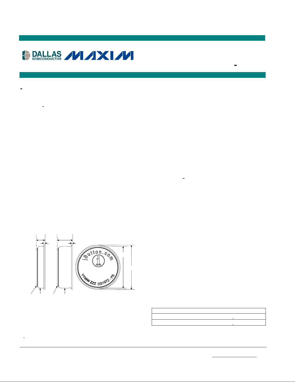
Button package. Data is written to an 8-
APPLICATIONS
Access Control/Parking Meter
Work-In-Progress Tracking
Tool Management
Inventory Control
Maintenance/Inspection Data Storage
F5 AND F3 MicroCAN
F3 size F5 size Branding
0.51
IO
5.89
GND
0.51
51 2D
0000006234FB
1-Wire
â
â
â
16.25
17.35
3.10
IO GND
Commands, Registers, and Modes are capitalized for
clarity.
Button, 1-Wire, and MicroCAN are registered trademarks of Dallas
I
Semiconductor Corp.
DS1972
1024-Bit EEPROM i
SPECIAL FEATURES
§ 1024 Bits of EEPROM Memory Partitioned into
Four Pages of 256 Bits
§ Individual Memory Pages can be Permanently
Write Protected or Put in EPROM-Emulation
Mode ("Write to 0")
§ Switchpoint Hysteresis and Filtering to Optimize
Performance in the Presence of Noise
§ IEC 1000-4-2 Level 4 ESD Protection (8kV
Contact, 15kV Air, typical)
§ Reads and Writes Over a Wide Voltage Range of
2.8V to 5.25V from -40°C to +85°C
§ Communicates to Host with a Single Digital
Signal at 15.4kbps or 125kbps Using 1-Wire
Protocol
COMMON iButton FEATURES
§ Unique Factory-Lasered 64-Bit Registration
Number Assures Error-Free Device Selection
and Absolute Traceability Because No Two Parts
are Alike
§ Built-In Multidrop Controller for 1-Wire Net
§ Chip-Based Data Carrier Stores Digital Identifi-
cation and Information, Armored in a Durable
Stainless-Steel Case
§ Data can be Accessed While Affixed to Object
§ Button Shape is Self-Aligning with Cup-Shaped
Probes
§ Easily Affixed with Self-Stick Adhesive Backing,
Latched by its Flange, or Locked with a Ring
Pressed onto its Rim
§ Presence Detector Acknowledges when Reader
First Applies Voltage
§ Designed to meet UL#913 (4th Edit.); Intrinsically
Safe Apparatus: Under Entity Concept for use in
Class I, Division 1, Group A, B, C, and D
Locations, contact Dallas Semiconductor for
certification schedule
ORDERING INFORMATION
PART TEMP RANGE PIN-PACKAGE
DS1972-F5# -40°C to 85°C F5 iButton
DS1972-F3# -40°C to 85°C F3 iButton
# indicates RoHS complience
Contact factory lead-free compliance
Button
Note: Some revisions of this device may incorporate deviations from published specifications known as errata. Multiple revisions of any device
may be simultaneously available through various sales channels. For information about device errata, click here: www.maxim-ic.com/errata
1 of 23 REV: 083006
.
Page 2

DS1972: 1024-Bit EEPROM iButton
ABSOLUTE MAXIMUM RATINGS
I/O Voltage to GND -0.5V, +6V
I/O Sink Current 20mA
Operating Temperature Range -40°C to +85°C
Junction Temperature +150°C
Storage Temperature Range -40°C to +85°C
Stresses beyond those listed under “Absolute Maximum Ratings” may cause permanent damage to the device. These are stress ratings only,
and functional operation of the device at these or any other conditions beyond those indicated in the operational sections of the specifications is
not implied. Exposure to the absolute maximum rating conditions for extended periods may affect device reliability.
ELECTRICAL CHARACTERISTICS
(TA = -40°C to +85°C; see Note 1.)
PARAMETER SYMBOL CONDITIONS MIN TYP MAX UNITS
I/O PIN GENERAL DATA
1-Wire Pullup Voltage V
1-Wire Pullup Resistance
PUP
R
PUP
(Notes 2) 2.8 5.25 V
(Notes 2, 3)
Input Capacitance CIO (Notes 4, 5) 1000 pF
Input Load Current I
High-to-Low Switching
Threshold
Input Low Voltage V
Low-to-High Switching
Threshold
Switching Hysteresis V
Output Low Voltage V
Recovery Time
(Notes 2,12)
(Notes 5, 13)
(Note 2, 14)
t
t
t
L
V
TL
IL
V
TH
HY
OL
REC
REH
SLOT
I/O pin at V
0.05 6.7 µA
PUP
(Notes 5, 6, 7) 0.46 4.4 V
(Notes 2, 8) 0.3 V
(Notes 5, 6, 9) 1.0 4.9 V
(Notes 5, 6, 10) 0.21 1.70 V
At 4mA (Note 11)
Standard speed, R
Overdrive speed, R
PUP
PUP
= 2.2kW
= 2.2kW
Overdrive speed, directly prior to Reset
Pulse; R
PUP
= 2.2kW
Standard speed 0.5 5.0 Rising-Edge Hold-off Time
Overdrive speed Not applicable (0)
Standard speed 65 Timeslot Duration
Overdrive speed 8
I/O PIN, 1-WIRE RESET, PRESENCE DETECT CYCLE
Reset Low Time (Note 2) t
Presence Detect High
Time
Presence Detect Low
Time
Presence Detect Sample
Time (Notes 2, 15)
RSTL
t
PDH
t
PDL
t
MSP
Standard speed 480 640
Overdrive speed 48 80
Standard speed 15 60
Overdrive speed 2 6
Standard speed 60 240
Overdrive speed 8 24
Standard speed 60 75
Overdrive speed 6 10
I/O PIN, 1-Wire WRITE
Write-0 Low Time (Notes
2, 16)
Write-1 Low Time
(Notes 2, 17)
t
W0L
t
W1L
Standard speed 60 120
Overdrive speed, V
> 4.5V 5 15.5
PUP
Overdrive speed 6 15.5
Standard speed 1
Overdrive speed 1
I/O PIN, 1-Wire READ
Read Low Time
(Notes 2, 18)
Read Sample Time
(Notes 2, 18)
t
t
MSR
RL
Standard speed 5
Overdrive speed 1
Standard speed
Overdrive speed
0.3 2.2
0.4 V
kW
5
2
µs
5
µs
µs
µs
µs
µs
µs
µs
15 - e
2 - e
µs
15 - d
2 - d
+ d
t
RL
+ d
t
RL
15
2
µs
µs
2 of 23
Page 3
DS1972: 1024-Bit EEPROM iButton
PARAMETER SYMBOL CONDITIONS MIN TYP MAX UNITS
EEPROM
Programming Current I
Programming Time t
durance) (Notes 21, 22)
Data Retention
(Notes 23, 24)
Note 1:
Note 2:
Note 3:
Note 4:
Note 5:
Note 6:
Note 7:
Note 8:
Note 9:
Note 10:
Note 11:
Note 12:
Note 13:
Note 14:
Note 15:
Note 16:
Note 17:
Note 18:
Note 19:
Note 20:
Note 21:
Note 22:
Note 23:
Note 24:
Specifications at T
= -40°C are guaranteed by design only and not production-tested.
A
System requirement.
Maximum allowable pullup resistance is a function of the number of 1-Wire devices in the system and 1-Wire recovery times. The
specified value here applies to systems with only one device and with the minimum 1-Wire recovery times. For more heavily
loaded systems, an active pullup such as that found in the DS2482-x00, DS2480B, or DS2490 may be required.
Maximum value represents the internal parasite capacitance when V
data line, 2.5µs after V
Guaranteed by design, characterization and/or simulation only. Not production tested.
V
, VTH, and V
TL
are a function of the internal supply voltage which is itself a function of V
HY
capacitive loading on IO. Lower V
and V
.
HY
Voltage below which, during a falling edge on IO, a logic 0 is detected.
The voltage on IO needs to be less or equal to V
Voltage above which, during a rising edge on IO, a logic 1 is detected.
After V
is crossed during a rising edge on IO, the voltage on IO has to drop by at least VHY to be detected as logic '0'.
TH
The I-V characteristic is linear for voltages less than 1V.
Applies to a single device attached to a 1-Wire line.
The earliest recognition of a negative edge is possible at t
Defines maximum possible bit rate. Equal to t
Interval after t
is t
PDH(max)
during which a bus master is guaranteed to sample a logic-0 on IO if there is a DS1972 present. Minimum limit
RSTL
; maximum limit is t
Highlighted numbers are NOT in compliance with legacy 1-Wire product standards. See comparison table below.
e represents the time required for the pullup circuitry to pull the voltage on IO up from V
d represents the time required for the pullup circuitry to pull the voltage on IO up from V
master.
Current drawn from IO during the EEPROM programming interval. The pullup circuit on IO during the programming interval
should be such that the voltage at IO is greater than or equal to Vpup(min). If Vpup in the system is close to Vpup(min) then a low
impedance bypass of Rpup which can be activated during programming may need to be added.
Interval begins t
WiLMIN
sequence. Interval ends once the device's self-timed EEPROM programming cycle is complete and the current drawn by the
device has returned from I
Write-cycle endurance is degraded as T
Not 100% production-tested; guaranteed by reliability monitor sampling.
Data retention is degraded as T
Guaranteed by 100% production test at elevated temperature for a shorter time; equivalence of this production test to data sheet
limit at operating temperature range is established by reliability testing.
PROG
PROG
N
CY
t
DR
has been applied the parasite capacitance will not affect normal communications.
PUP
PDH(min)
(Note 5, 19) 0.8 mA
(Note 20) 10 ms
At 25°C 200k Write/Erase Cycles (EnAt 85°C (worst case) 50k
At 85°C (worst case) 10
is first applied. If a 2.2kW resistor is used to pull up the
PUP
, higher R
PUP
+ t
PDL(min)
W0L(min)
.
, shorter t
PUP
IL(MAX)
+ t
, and heavier capacitive loading all lead to lower values of VTL, VTH,
REC
at all times the master is driving IO to a logic-0 level.
after VTH has been reached on the preceding rising edge.
REH
.
REC(min)
after the leading negative edge on IO for the last timeslot of the E/S byte for a valid Copy Scratchpad
to IL.
PROG
A
increases.
A
increases.
---
, R
PUP
to VTH.
IL
to the input high threshold of the bus
IL
, 1-Wire timing, and
PUP
years
LEGACY VALUES DS1972 VALUES
PARAMETER STANDARD SPEED OVERDRIVE SPEED STANDARD SPEED OVERDRIVE SPEED
MIN MAX MIN MAX MIN MAX MIN MAX
t
(incl. t
SLOT
t
RSTL
t
PDH
t
PDL
t
W0L
1)
Intentional change, longer recovery time requirement due to modified 1-Wire front end.
REC)
61µs (undef.) 7µs (undef.) 65µs1) (undef.) 8µs1) (undef.)
480µs (undef.) 48µs 80µs 480µs 640µs 48µs 80µs
15µs 60µs 2µs 6µs 15µs 60µs 2µs 6µs
60µs 240µs 8µs 24µs 60µs 240µs 8µs 24µs
60µs 120µs 6µs 16µs 60µs 120µs 6µs 15.5µs
EXAMPLES OF ACCESSORIES
PART DESCRIPTION
DS9096P Self-Stick Adhesive Pad
DS9101 Multipurpose Clip
DS9093RA Mounting Lock Ring
DS9093A Snap-In Fob
DS9092 iButton Probe
3 of 23
Page 4
DS1972: 1024-Bit EEPROM iButton
DESCRIPTION
The DS1972 combines 1024 bits of EEPROM, an 8-byte register/control page with up to 7 user read/write bytes,
and a fully-featured 1-Wire interface in a rugged i
registration number that is factory lasered to provide a guaranteed unique identity for absolute traceability. Data is
transferred serially via the 1-Wire protocol, which requires only a single data contact and a ground return. The
DS1972 has an additional memory area called the scratchpad that acts as a buffer when writing to the main
memory or the register page. Data is first written to the scratchpad from which it can be read back. After the data
has been verified, a Copy Scratchpad command transfers the data to its final memory location. Applications of the
DS1972 include access control/parking meter, Work-In-Progress tracking, tool management, inventory control, and
maintenance/inspection data storage. Software for communication with the DS1972 is available for free download
from the http://www.maxim-ic.com/products/ibutton/ website.
Button package. Each DS1972 has its own 64-bit ROM
OVERVIEW
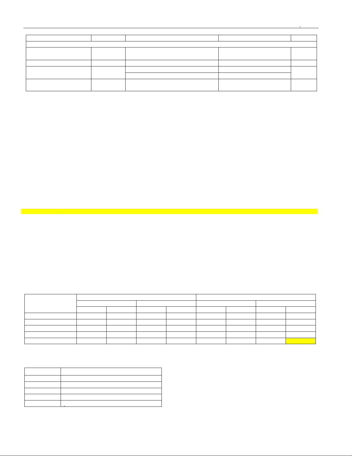
The block diagram in Figure 1 shows the relationships between the major control and memory sections of the
DS1972. The DS1972 has four main data components: 1) 64-bit lasered ROM, 2) 64-bit scratchpad, 3) four 32-byte
pages of EEPROM, and 4) 64-bit register page. The hierarchical structure of the 1-Wire protocol is shown in Figure
2. The bus master must first provide one of the seven ROM Function Commands, 1) Read ROM, 2) Match ROM, 3)
Search ROM, 4) Skip ROM, 5) Resume, 6) Overdrive-Skip ROM or 7) Overdrive-Match ROM. Upon completion of
an Overdrive ROM command byte executed at standard speed, the device enters Overdrive mode where all
subsequent communication occurs at a higher speed. The protocol required for these ROM function commands is
described in Figure 9. After a ROM function command is successfully executed, the memory functions become
accessible and the master may provide any one of the four memory function commands. The protocol for these
memory function commands is described in Figure 7. All data is read and written least significant bit first.
Figure 1. Block Diagram
PARASITE POWER
I/O
Memory
Function
Control Unit
CRC16
Generator
Data Memory
4 Pages of
256 bits each
Register Page
64 bits
1-Wire
Function Control
4 of 23
64-bit
Lasered ROM
DS1972
64-bit
Scratchpad
Page 5
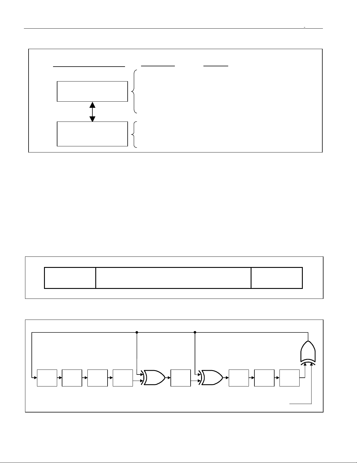
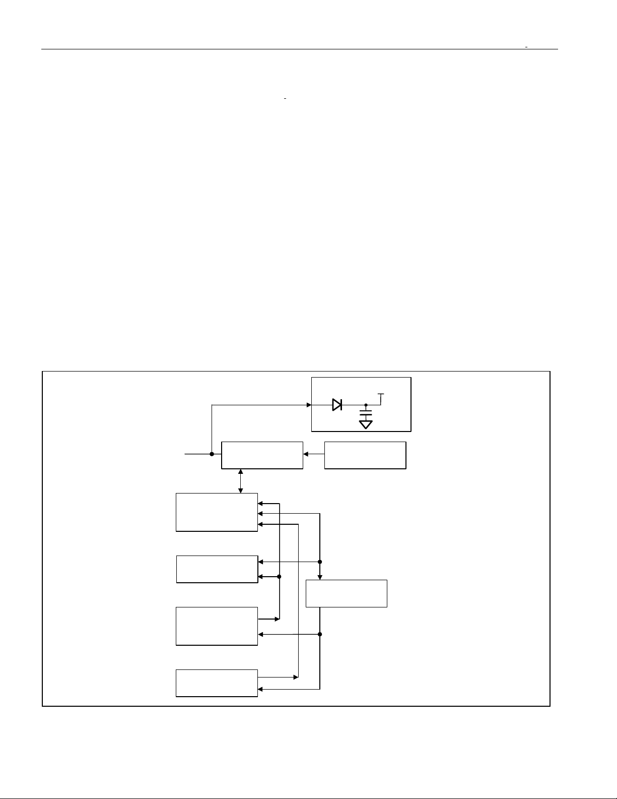
Figure 2. Hierarchical Structure for 1-Wire Protocol
A
A
DS1972 Command Level:
1-Wire ROM Function
Commands (see Figure 9)
vailable
Commands:
Read ROM
Match ROM
Search ROM
Skip ROM
Resume
Overdrive-Skip
Overdrive-Match
DS1972: 1024-Bit EEPROM iButton
Data Field
ffected:
64-bit Reg. #, RC-Flag
64-bit Reg. #, RC-Flag
64-bit Reg. #, RC-Flag
RC-Flag
RC-Flag
RC-Flag, OD-Flag
64-bit Reg. #, RC-Flag, OD-Flag
DS1972-specific
Memory Function
Commands (see Figure 7)
Write Scratchpad
Read Scratchpad
Copy Scratchpad
Read Memory
64-bit Scratchpad, Flags
64-bit Scratchpad
Data Memory, Register Page
Data Memory, Register Page
64-BIT LASERED ROM
Each DS1972 contains a unique ROM code that is 64 bits long. The first 8 bits are a 1-Wire family code. The next
48 bits are a unique serial number. The last 8 bits are a CRC (Cyclic Redundancy Check) of the first 56 bits. See
Figure 3 for details. The 1-Wire CRC is generated using a polynomial generator consisting of a shift register and
XOR gates as shown in Figure 4. The polynomial is X
CRC is available in Application Note 27.
The shift register bits are initialized to 0. Then starting with the least significant bit of the family code, one bit at a
time is shifted in. After the 8th bit of the family code has been entered, then the serial number is entered. After the
last bit of the serial number has been entered, the shift register contains the CRC value. Shifting in the 8 bits of the
CRC returns the shift register to all 0s.
Figure 3. 64-Bit Lasered ROM
MSB LSB
8-Bit
CRC Code
MSB LSB MSB LSB MSB LSB
Figure 4. 1-Wire CRC Generator
Polynomial = X8 + X5 + X4 + 1
8
+ X5 + X4 + 1. Additional information about the Dallas 1-Wire
48-Bit Serial Number
8-Bit Family
Code (2Dh)
STAGE
0
X
st
1
STAGE
1
X
nd
2
2
X
rd
3
STAGE
STAGE
3
X
th
4
4
X
th
5
STAGE
5
X
th
6
STAGE
INPUT DATA
6
X
th
7
STAGE
STAGE
7
X
th
8
8
X
5 of 23
Page 6

DS1972: 1024-Bit EEPROM iButton
Figure 5. Memory Map
ADDRESS RANGE TYPE DESCRIPTION PROTECTION CODES
0000h to 001Fh R/(W) Data Memory Page 0
0020h to 003Fh R/(W) Data Memory Page 1
0040h to 005Fh R/(W) Data Memory Page 2
0060h to 007Fh R/(W) Data Memory Page 3
0080h1) R/(W) Protection Control Byte
Page 0
0081h1) R/(W) Protection Control Byte
Page 1
0082h1) R/(W) Protection Control Byte
Page 2
0083h1) R/(W) Protection Control Byte
Page 3
0084h1) R/(W) Copy Protection Byte 55h or AAh: Copy Protect 0080:008Fh, and
0085h R Factory byte. Set at
Factory.
0086h R/(W) User Byte/Manufacturer ID
0087h R/(W) User Byte/Manufacturer ID
0088h to 008Fh N/A Reserved
1)
Once programmed to AAh or 55h this address becomes read-only. All other codes can be stored but will neither
write-protect the address nor activate any function.
55h: Write Protect P0; AAh: EPROM mode
P0; 55h or AAh: Write Protect 80h
55h: Write Protect P1; AAh: EPROM mode
P1; 55h or AAh: Write Protect 81h
55h: Write Protect P2; AAh: EPROM mode
P2; 55h or AAh: Write Protect 82h
55h: Write Protect P3; AAh: EPROM mode
P3; 55h or AAh: Write Protect 83h
any write-protected Pages
AAh:Write Protect 85h, 86h, 87h;
55h: Write Protect 85h, unprotect 86h, 87h
MEMORY
Data memory and registers are located in a linear address space, as shown in Figure 5. The data memory and the
registers have unrestricted read access. The DS1972 EEPROM array consists of 18 rows of 8 bytes each. The first
16 rows are divided equally into 4 memory pages (32 bytes each). These 4 pages are the primary data memory.
Each page can be individually set to Open (unprotected), Write-Protected, or EPROM mode by setting the
associated protection byte in the register row. The last two rows contain protection registers, and reserved bytes.
The register row consists of 4 protection control bytes, a copy protection byte, the factory byte, and two user
byte/manufacture ID bytes. The manufacturer ID can be a customer-supplied identification code that assists the
application software in identifying the product the DS1972 is associated with. Contact the factory to set up and
register a custom manufacturer ID. The last row is reserved for future use. It is undefined in terms of R/W
functionality and should not be used.
In addition to the main EEPROM array, an 8-byte volatile scratchpad is included. Writes to the EEPROM array are
a two-step process. First, data is written to the scratchpad, and then copied into the main array. This allows the
user to first verify the data written to scratchpad prior to copying into the main array. The device only supports full
row (8-byte) copy operations. In order for data in the scratchpad to be valid for a copy operation, the address
supplied with a Write Scratchpad must start on a row boundary, and 8 full bytes must be written into the
scratchpad.
6 of 23
Page 7

DS1972: 1024-Bit EEPROM iButton
The protection control registers determine how incoming data on a Write Scratchpad command is loaded into the
scratchpad. A protection setting of 55h (Write Protect) causes the incoming data to be ingnored and the target
address main memory data to be loaded into the scratchpad. A protection setting of AAh (EPROM mode) causes
the logical AND of incoming data and target address main memory data to be loaded into the scratchpad. Any
other protection control register setting leaves the associated memory page open for unrestricted write access.
Protection control byte settings of 55h or AAh also write protects the protection control byte. The protection-control
byte setting of 55h does not block the copy. This allows write-protected data to be refreshed (i. e., reprogrammed
with the current data) in the device.
The copy protection byte is used for a higher level of security, and should only be used after all other protection
control bytes, user bytes, and write-protected pages are set to their final value. If the copy protection byte is set to
55h or AAh, all copy attempts to the register row and user byte row are blocked. In addition, all copy attempts to
write-protected main memory pages (i. e., refresh) are blocked.
ADDRESS REGISTERS AND TRANSFER STATUS
The DS1972 employs three address registers: TA1, TA2, and E/S (Figure 6). These registers are common to many
other 1-Wire devices but operate slightly differently with the DS1972. Registers TA1 and TA2 must be loaded with
the target address to which the data is written or from which data is read. Register E/S is a read-only transferstatus register, used to verify data integrity with write commands. E/S bits E2:E0 are loaded with the incoming
T2:T0 on a Write Scratchpad command, and increment on each subsequent data byte. This is in effect a byteending offset counter within the 8-byte scratchpad. Bit 5 of the E/S register, called PF, is a logic 1 if the data in the
scratchpad is not valid due to a loss of power or if the master sends less bytes than needed to reach the end of the
scratchpad. For a valid write to the scratchpad, T2:T0 must be 0 and the master must have sent 8 data bytes. Bits
3, 4, and 6 have no function; they always read 0. The highest valued bit of the E/S register, called AA or
Authorization Accepted, acts as a flag to indicate that the data stored in the scratchpad has already been copied to
the target memory address. Writing data to the scratchpad clears this flag.
Figure 6. Address Registers
Bit # 7 6 5 4 3 2 1 0
Target Address (TA1) T7 T6 T5 T4 T3 T2 T1 T0
Target Address (TA2) T15 T14 T13 T12 T11 T10 T9 T8
Ending Address with
Data Status (E/S)
(Read Only)
AA 0 PF 0 0 E2 E1 E0
7 of 23
Page 8

DS1972: 1024-Bit EEPROM iButton
WRITING WITH VERIFICATION
To write data to the DS1972, the scratchpad has to be used as intermediate storage. First the master issues the
Write Scratchpad command to specify the desired target address, followed by the data to be written to the
scratchpad. Note that Copy Scratchpad commands must be performed on 8-byte boundaries, i. e., the 3 LSBs of
the target address (T2..T0) must be equal to 000b. If T2..T0 are sent with non-zero values, the copy function will be
blocked. Under certain conditions (see Write Scratchpad command) the master will receive an inverted CRC16 of
the command, address (actual address sent) and data at the end of the Write Scratchpad command sequence.
Knowing this CRC value, the master can compare it to the value it has calculated itself to decide if the
communication was successful and proceed to the Copy Scratchpad command. If the master could not receive the
CRC16, it should send the Read Scratchpad command to verify data integrity. As a preamble to the scratchpad
data, the DS1972 repeats the target address TA1 and TA2 and sends the contents of the E/S register. If the PF
flag is set, data did not arrive correctly in the scratchpad or there was a loss of power since data was last written to
the scratchpad. The master does not need to continue reading; it can start a new trial to write data to the
scratchpad. Similarly, a set AA flag together with a cleared PF flag indicates that the device did not recognize the
Write command. If everything went correctly, both flags are cleared. Now the master can continue reading and
verifying every data byte. After the master has verified the data, it can send the Copy Scratchpad command, for
example. This command must be followed exactly by the data of the three address registers, TA1, TA2, and E/S.
The master should obtain the contents of these registers by reading the scratchpad.
MEMORY FUNCTION COMMANDS
The Memory Function Flow Chart (Figure 7) describes the protocols necessary for accessing the memory of the
DS1972. An example on how to use these functions to write to and read from the device is included at the end of
this document. The communication between master and DS1972 takes place either at regular speed (default, OD =
0) or at Overdrive Speed (OD = 1). If not explicitly set into the Overdrive mode, the DS1972 assumes regular
speed.
WRITE SCRATCHPAD COMMAND [0Fh]
The Write Scratchpad command applies to the data memory, and the writable addresses in the register page. In
order for the scratchpad data to be valid for copying to the array, the user must perform a Write Scratchpad
command of 8 bytes starting at a valid row boundary. The Write Scratchpad command accepts invalid addresses,
and partial rows, but subsequent Copy Scratchpad commands are blocked.
After issuing the Write Scratchpad command, the master must first provide the 2-byte target address, followed by
the data to be written to the scratchpad. The data is written to the scratchpad starting at the byte offset of T2:T0.
The E/S bits E2:E0 are loaded with the starting byte offset, and increment with each susequent byte. Effectively,
E2:E0 is the byte offset of the last full byte written to the scratchpad. Only full data bytes are accepted.
When executing the Write Scratchpad command, the CRC generator inside the DS1972 (Figure 13) calculates a
CRC of the entire data stream, starting at the command code and ending at the last data byte as sent by the
master. This CRC is generated using the CRC16 polynomial by first clearing the CRC generator and then shifting
in the command code (0Fh) of the Write Scratchpad command, the Target Addresses (TA1 and TA2), and all the
data bytes. Note that the CRC16 calculation is performed with the actual TA1 and TA2 and data sent by the
master. The master may end the Write Scratchpad command at any time. However, if the end of the scratchpad is
reached (E2:E0 = 111b), the master may send 16 read-time slots and receive the CRC generated by the DS1972.
If a Write Scratchpad is attempted to a write-protected location, the scratchpad is loaded with the data already in
memory, rather than the data transmitted. Similarly, if the target address page is in EPROM mode, the scratchpad
is loaded with the bitwise logical AND of the transmitted data and data already in memory.
8 of 23
Page 9

Figure 7-1. Memory Function Flow Chart
A
p
Bus Master TX Memory
Function Command
0Fh
Write Scratch-
pad ?
Y
Bus Master TX
TA1 (T7:T0), TA2 (T15:T8)
DS1972 sets
Sets PF = 1
Clears AA = 0
Sets E2:E0 = T2:T0
DS1972: 1024-Bit EEPROM iButton
From ROM Functions
Flow Chart (Figure 9)
To Figure 7
nd
2
N
Part
DS1972
Increments
E2:E0
Master TX Data Byte
To Scratchpad
Master
TX Reset ?
N
E2:E0
N
of Command, Address,
Data Bytes as they were
sent by the bus master
= 7 ?
Y
T2:T0
= 0 ?
Y
PF = 0
DS1972 TX CRC16
pplies only if the
memory area is not
rotected.
Y
N
If write-protected, then
the DS1972 copies the
data byte from the target address into the SP.
If in EPROM mode,
then the DS1972 loads
the bitwise logical AND
of the transmitted byte
and the data byte from
the targeted address
into the SP.
Bus Master
RX “1”s
N
Master
TX Reset ?
Y
To ROM Functions
Flow Chart (Figure 9)
From Figure 7
nd
2
Part
9 of 23
Page 10

Figure 7-2. Memory Function Flow Chart (continued)
y
DS1972: 1024-Bit EEPROM iButton
From Figure 7
st
1
Part
DS1972
Increments
B
te Counter
AAh
Read Scratch-
Pad ?
Y
Bus Master RX
TA1 (T7:T0), TA2 (T15:T8)
and E/S Byte
DS1972 sets Scratchpad
Byte Counter = T2:T0
Bus Master RX
Data Byte from Scratchpad
Master
Y
TX Reset ?
N
N
Byte Counter
= E2:E0 ?
To Figure 7
N
rd
3
Part
To Figure 7
st
1
Part
Bus Master
RX “1”s
Y
Bus Master RX CRC16
of Command, Address,
E/S Byte, Data Bytes as
sent by the DS1972
N
Master
TX Reset ?
Y
From Figure 7
rd
3
Part
10 of 23
Page 11
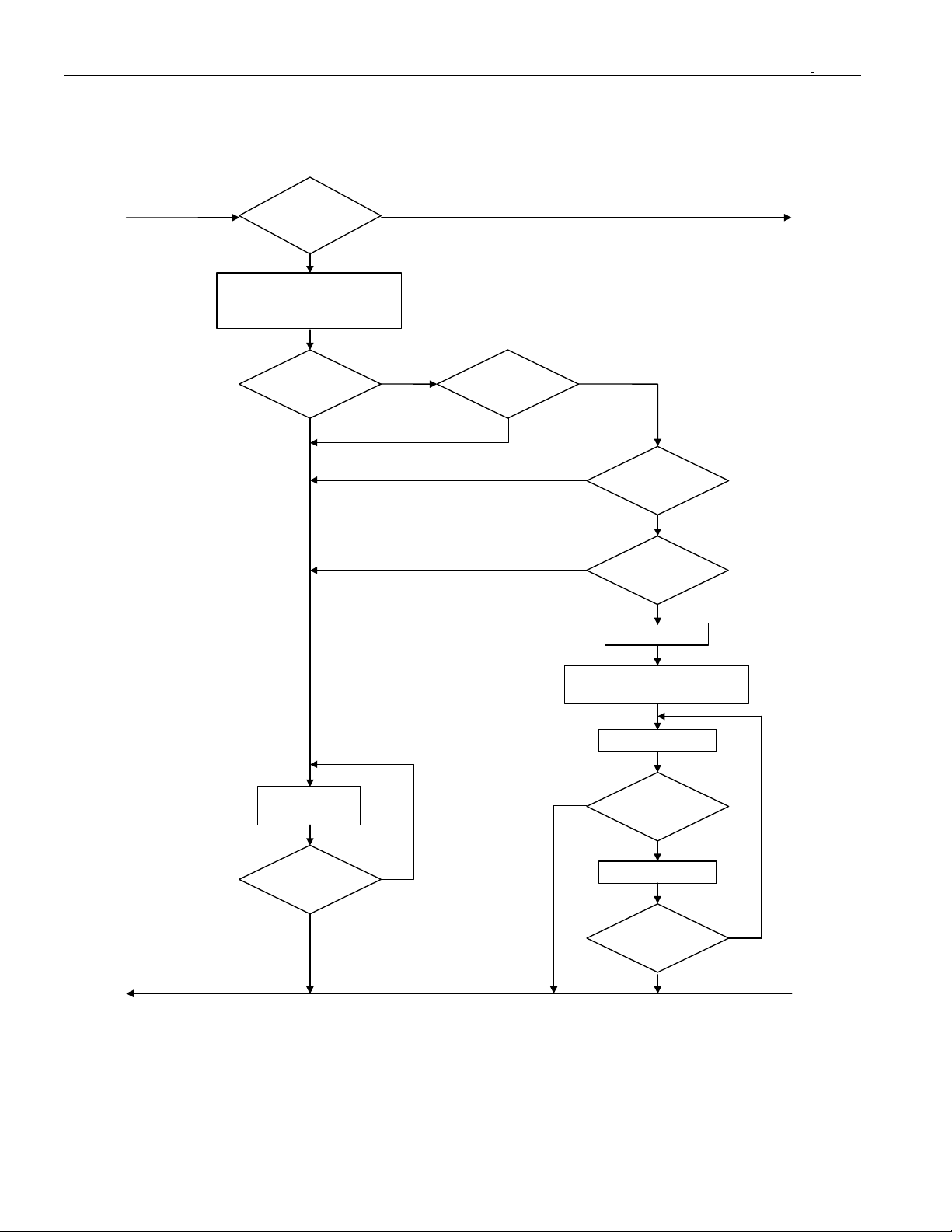
Figure 7-3. Memory Function Flow Chart (continued)
A
DS1972: 1024-Bit EEPROM iButton
From Figure 7
nd
2
Part
TA1 (T7:T0), TA2 (T15:T8)
55h
Copy Scratch-
Pad ?
Y
Bus Master TX
and E/S Byte
Auth. Code
Match ?
N
To Figure 7
N
4
th
Part
pplicable to all R/W
memory locations.
Y
T15:T0
Y
< 0090h ?
N
N
PF = 0 ?
Y
Y
Copy-
Protected ?
N
AA = 1
Duration: t
Bus Master
RX “1”s
Master
N
TX Reset ?
Y
To Figure 7
nd
2
Part
* 1-Wire idle high for power
11 of 23
PROG
DS1972 copies Scratch-
pad Data to Address
DS1972 TX “0”
Y
Master
TX Reset ?
N
DS1972 TX “1”
Master
TX Reset ?
Y
From Figure 7
th
4
Part
*
N
Page 12

Figure 7-4. Memory Function Flow Chart (continued)
From Figure 7
3
rd
Part
F0h
Read Memory ?
Y
Bus Master TX
TA1 (T7:T0),
TA2 (T15:T8)
N
DS1972: 1024-Bit EEPROM iButton
Address
< 90h ?
N
DS1972
Increments
Address
Y
Counter
DS1972 sets Memory
Address = (T15:T0)
Bus Master RX
Data Byte from
Memory Address
Master
TX Reset ?
N
Y
Address
< 8Fh ?
N
Y
Bus Master
RX “1”s
N
TX Reset ?
To Figure 7
rd
3
Part
Bus Master
RX “1”s
12 of 23
Master
N
Y
Master
TX Reset ?
Y
Page 13

DS1972: 1024-Bit EEPROM iButton
READ SCRATCHPAD COMMAND [AAh]
The Read Scratchpad command allows verifying the target address and the integrity of the scratchpad data. After
issuing the command code, the master begins reading. The first two bytes are the target address. The next byte is
the ending offset/data status byte (E/S) followed by the scratchpad data, which may be different from what the
master originally sent. This is of particular importance if the target address is within the register page or a page in
either Write Protection or EPROM modes. See the Write Scratchpad description for details. The master should
read through the scratchpad (E2:E0 - T2:T0 + 1 bytes), after which it will receive the inverted CRC, based on data
as it was sent by the DS1972. If the master continues reading after the CRC, all data will be logic 1s.
COPY SCRATCHPAD [55h]
The Copy Scratchpad command is used to copy data from the scratchpad to writable memory sections. After
issuing the Copy Scratchpad command, the master must provide a 3-byte authorization pattern, which should have
been obtained by an immediately preceding Read Scratchpad command. This 3-byte pattern must exactly match
the data contained in the three address registers (TA1, TA2, E/S, in that order). If the pattern matches, the target
address is valid, the PF flag is not set, and the target memory is not copy-protected, the AA (Authorization
Accepted) flag is set and the copy begins. All eight bytes of scratchpad contents are copied to the target memory
location. The duration of the device’s internal data transfer is t
not fall below 2.8V. A pattern of alternating 0s and 1s are transmitted after the data has been copied until the
master issues a Reset Pulse. If the PF flag is set or the target memory is copy-protected, the copy will not begin
and the AA flag will not be set. If the copy command was disturbed due to lack of power or for other reasons, the
master will read a constant stream of FFh bytes until it sends a 1-Wire Reset Pulse. In this case the destination
memory may be incompletely programmed requiring a write scratchpad and copy scratchpad be repeated to
ensure proper programming of the EEPROM. This requires careful consideration when designing application
software that writes to the DS1972 in an intermittent contact environment.
during which the voltage on the 1-Wire bus must
PROG
READ MEMORY [F0h]
The Read Memory command is the general function to read data from the DS1972. After issuing the command, the
master must provide the 2-byte target address. After these two bytes, the master reads data beginning from the
target address and may continue until address 008Fh. If the master continues reading, the result will be logic 1s.
The device's internal TA1, TA2, E/S, and scratchpad contents are not affected by a Read Memory command.
1-Wire BUS SYSTEM
The 1-Wire bus is a system that has a single bus master and one or more slaves. In all instances the DS1972 is a
slave device. The bus master is typically a microcontroller. The discussion of this bus system is broken down into
three topics: hardware configuration, transaction sequence, and 1-Wire signaling (signal types and timing). The
1-Wire protocol defines bus transactions in terms of the bus state during specific time slots, which are initiated on
the falling edge of sync pulses from the bus master.
HARDWARE CONFIGURATION
The 1-Wire bus has only a single line by definition; it is important that each device on the bus be able to drive it at
the appropriate time. To facilitate this, each device attached to the 1-Wire bus must have open-drain or tri-state
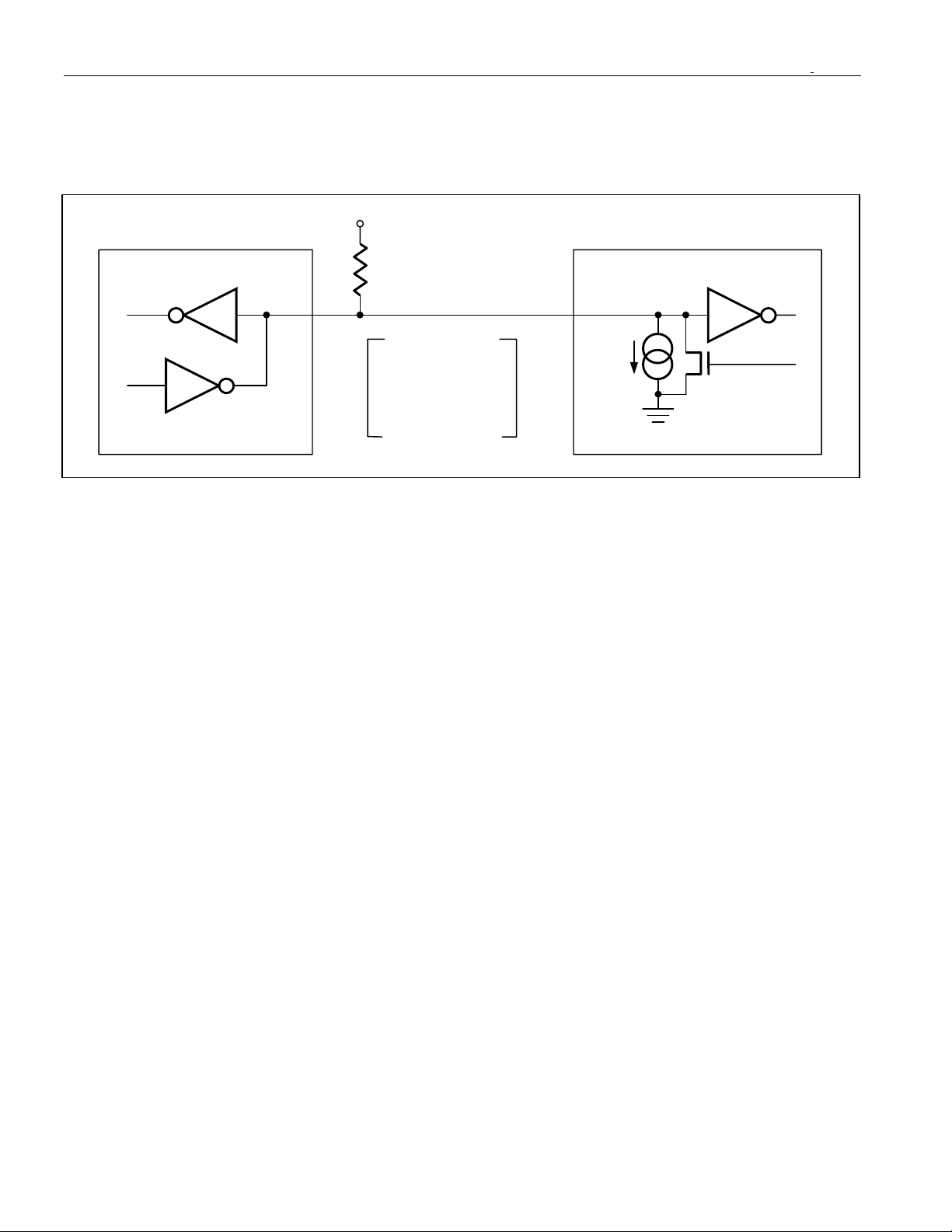
outputs. The 1-Wire port of the DS1972 is open drain with an internal circuit equivalent to that shown in Figure 8.
A multidrop bus consists of a 1-Wire bus with multiple slaves attached. The DS1972 supports both a Standard and
Overdrive communication speed of 15.4kbps (max) and 125kbps (max), respectively. Note that legacy 1-Wire
products support a standard communication speed of 16.3kbps and Overdrive of 142kbps. The slightly reduced
rates for the DS1972 are a result of additional recovery times, which in turn were driven by a 1-Wire physical
interface enhancement to improve noise immunity. The value of the pullup resistor primarily depends on the
network size and load conditions. The DS1972 requires a pullup resistor of 2.2kW (max) at any speed.
13 of 23
Page 14
DS1972: 1024-Bit EEPROM iButton
The idle state for the 1-Wire bus is high. If for any reason a transaction needs to be suspended, the bus MUST be
left in the idle state if the transaction is to resume. If this does not occur and the bus is left low for more than 16µs
(Overdrive speed) or more than 120µs (standard speed), one or more devices on the bus may be reset.
Figure 8. Hardware Configuration
BUS MASTER DS1972 1-Wire PORT
V
PUP
R
PUP
RX
TX
Open Drain
Port Pin
RX = RECEIVE
TX = TRANSMIT
I
L
100
MOSFET
RXDATA
TX
W
TRANSACTION SEQUENCE
The protocol for accessing the DS1972 through the 1-Wire port is as follows:
§ Initialization
§ ROM Function Command
§ Memory Function Command
§ Transaction/Data
INITIALIZATION
All transactions on the 1-Wire bus begin with an initialization sequence. The initialization sequence consists of a
Reset Pulse transmitted by the bus master followed by Presence Pulse(s) transmitted by the slave(s). The
Presence Pulse lets the bus master know that the DS1972 is on the bus and is ready to operate. For more details,
see the 1-Wire Signaling section.
1-Wire ROM FUNCTION COMMANDS
Once the bus master has detected a presence, it can issue one of the seven ROM function commands that the
DS1972 supports. All ROM function commands are 8 bits long. A list of these commands follows (refer to the flow
chart in Figure 9).
READ ROM [33h]
This command allows the bus master to read the DS1972’s 8-bit family code, unique 48-bit serial number, and 8-bit
CRC. This command can only be used if there is a single slave on the bus. If more than one slave is present on the
bus, a data collision occurs when all slaves try to transmit at the same time (open drain produces a wired-AND
result). The resultant family code and 48-bit serial number result in a mismatch of the CRC.
MATCH ROM [55h]
The Match ROM command, followed by a 64-bit ROM sequence, allows the bus master to address a specific
DS1972 on a multidrop bus. Only the DS1972 that exactly matches the 64-bit ROM sequence responds to the
following memory function command. All other slaves wait for a Reset Pulse. This command can be used with a
single or multiple devices on the bus.
14 of 23
Page 15

DS1972: 1024-Bit EEPROM iButton
SEARCH ROM [F0h]
When a system is initially brought up, the bus master might not know the number of devices on the 1-Wire bus or
their registration numbers. By taking advantage of the wired-AND property of the bus, the master can use a
process of elimination to identify the registration numbers of all slave devices. For each bit of the registration
number, starting with the least significant bit, the bus master issues a triplet of time slots. On the first slot, each
slave device participating in the search outputs the true value of its registration number bit. On the second slot,
each slave device participating in the search outputs the complemented value of its registration number bit. On the
third slot, the master writes the true value of the bit to be selected. All slave devices that do not match the bit
written by the master stop participating in the search. If both of the read bits are zero, the master knows that slave
devices exist with both states of the bit. By choosing which state to write, the bus master branches in the romcode
tree. After one complete pass, the bus master knows the registration number of a single device. Additional passes
identify the registration numbers of the remaining devices. Refer to Application Note 187: 1-Wire Search Algorithm
for a detailed discussion, including an example.
SKIP ROM [CCh]
This command can save time in a single-drop bus system by allowing the bus master to access the memory
functions without providing the 64-bit ROM code. If more than one slave is present on the bus and, for example, a
Read command is issued following the Skip ROM command, data collision occurs on the bus as multiple slaves
transmit simultaneously (open-drain pulldowns produce a wired-AND result).
RESUME [A5h]
To maximize the data throughput in a multidrop environment, the Resume function is available. This function
checks the status of the RC bit and, if it is set, directly transfers control to the memory functions, similar to a Skip
ROM command. The only way to set the RC bit is through successfully executing the Match ROM, Search ROM, or
Overdrive-Match ROM command. Once the RC bit is set, the device can repeatedly be accessed through the
Resume Command function. Accessing another device on the bus clears the RC bit, preventing two or more
devices from simultaneously responding to the Resume Command function.
OVERDRIVE-SKIP ROM [3Ch]
On a single-drop bus this command can save time by allowing the bus master to access the memory functions
without providing the 64-bit ROM code. Unlike the normal Skip ROM command, the Overdrive-Skip ROM sets the
DS1972 in the Overdrive mode (OD = 1). All communication following this command has to occur at Overdrive
speed until a Reset Pulse of minimum 480µs duration resets all devices on the bus to standard speed (OD = 0).
When issued on a multidrop bus, this command sets all Overdrive-supporting devices into Overdrive mode. To
subsequently address a specific Overdrive-supporting device, a Reset Pulse at Overdrive speed has to be issued
followed by a Match ROM or Search ROM command sequence. This speeds up the time for the search process. If
more than one slave supporting Overdrive is present on the bus and the Overdrive-Skip ROM command is followed
by a Read command, data collision occurs on the bus as multiple slaves transmit simultaneously (open-drain
pulldowns produce a wired-AND result).
OVERDRIVE-MATCH ROM [69h]
The Overdrive-Match ROM command followed by a 64-bit ROM sequence transmitted at Overdrive Speed allows
the bus master to address a specific DS1972 on a multidrop bus and to simultaneously set it in Overdrive mode.
Only the DS1972 that exactly matches the 64-bit ROM sequence responds to the subsequent memory function
command. Slaves already in Overdrive mode from a previous Overdrive-Skip or successful Overdrive-Match
command remain in Overdrive mode. All overdrive-capable slaves return to standard speed at the next Reset Pulse
of minimum 480µs duration. The Overdrive-Match ROM command can be used with a single or multiple devices on
the bus.
15 of 23
Page 16

Figure 9-1. ROM Functions Flow Chart
YNY
Y
YNY
Y
YYY
Y
Y
d
Bus Master TX
Reset Pulse
From Memory Functions
Flow Chart (Figure 7)
Reset Pulse ?
OD
N
OD = 0
DS1972: 1024-Bit EEPROM iButton
From Figure 9, 2
n
Part
Bus Master TX ROM
Function Command
33h
Read ROM
Command ?
RC = 0
DS1972 TX
Family Code
(1 Byte)
DS1972 TX
Serial Number
(6 Bytes)
N
55h
Match ROM
Command ?
RC = 0
Master TX Bit 0
Bit 0
Match ?
Master TX Bit 1
Bit 1
Match ?
DS1972 TX
Presence Pulse
N
N
N
F0h
Search ROM
Command ?
RC = 0
DS1972 TX Bit 0
DS1972 TX Bit 0
Master TX Bit 0
Bit 0
Match ?
DS1972 TX Bit 1
DS1972 TX Bit 1
Master TX Bit 1
Bit 1
Match ?
To Figure 9
N
CCh
nd
Part
2
Skip ROM
Command ?
N
RC = 0
DS1972 TX
CRC Byte
Master TX Bit 63
DS1972 TX Bit 63
Master TX Bit 63
DS1972 TX Bit 63
Bit 63
Match ?
RC = 1
N
To Memory Functions
Flow Chart (Figure 7)
Bit 63
Match ?
RC = 1
To Figure 9
nd
Part
2
From Figure 9
nd
Part
2
N
16 of 23
Page 17

Figure 9-2. ROM Functions Flow Chart (continued)
t
DS1972: 1024-Bit EEPROM iButton
To Figure 9, 1
From Figure 9
st
1
Part
s
Part
Resume
Command ?
RC = 1 ?
A5h
Y
Y
N
N
3Ch
Overdrive-
Skip ROM ?
Y
RC = 0 ; OD = 1
Master
TX Reset ?
N
N
69h
N
Overdrive-Match
ROM ?
Y
RC = 0 ; OD = 1
Master TX Bit 0
Y
Bit 0
Match ?
N
OD = 0
Y
From Figure 9
st
Part
1
To Figure 9
st
1
Part
Master
TX Reset ?
N
Master TX Bit 1
Y
Bit 1
Match ?
N
OD = 0
Y
Master TX Bit 63
Bit 63
Match ?
N
OD = 0
Y
RC = 1
17 of 23
Page 18

DS1972: 1024-Bit EEPROM iButton
1-Wire SIGNALING
The DS1972 requires strict protocols to ensure data integrity. The protocol consists of four types of signaling on
one line: Reset Sequence with Reset Pulse and Presence Pulse, Write-Zero, Write-One, and Read-Data. Except
for the Presence Pulse, the bus master initiates all falling edges. The DS1972 can communicate at two different
speeds, standard speed, and Overdrive Speed. If not explicitly set into the Overdrive mode, the DS1972
communicates at standard speed. While in Overdrive mode the fast timing applies to all waveforms.
To get from idle to active, the voltage on the 1-Wire line needs to fall from V
from active to idle, the voltage needs to rise from V
past the threshold VTH. The time it takes for the voltage to
ILMAX
make this rise is seen in Figure 10 as 'e' and its duration depends on the pullup resistor (R
capacitance of the 1-Wire network attached.
The voltage V
is relevant for the DS1972 when determining a
ILMAX
logical level, not triggering any events.
Figure 10 shows the initialization sequence required to begin any communication with the DS1972. A Reset Pulse
followed by a Presence Pulse indicates the DS1972 is ready to receive data, given the correct ROM and memory
function command. If the bus master uses slew-rate control on the falling edge, it must pull down the line for
t
+ tF to compensate for the edge. A t
RSTL
device to standard speed. If the DS1972 is in Overdrive mode and t
in Overdrive mode. If the device is in Overdrive mode and t
duration of 480µs or longer exits the Overdrive mode, returning the
RSTL
is between 80µs and 480µs, the device will reset,
RSTL
is no longer than 80µs. the device remains
RSTL
but the communication speed is undetermined.
Figure 10. Initialization Procedure: Reset and Presence Pulse
MASTER TX “RESET PULSE” MASTER RX “PRESENCE PULSE”
below the threshold VTL. To get
PUP
) used and the
PUP
t
MSP
V
IHMASTER
V
V
PUP
V
TH
V
ILMAX
e
TL
0V
t
F
t
RSTL
t
PDH
t
PDL
t
RSTH
t
REC
RESISTOR MASTER DS1972
After the bus master has released the line it goes into Receive mode. Now the 1-Wire bus is pulled to V
the pullup resistor, or in case of a DS2482-x00 or DS2480B driver, by active circuitry. When the threshold V
crossed, the DS1972 waits for t
Presence Pulse, the master must test the logical state of the 1-Wire line at t
and then transmits a Presence Pulse by pulling the line low for t
PDH
MSP
.
PDL
through
PUP
TH
is
. To detect a
The t
DS1972 is ready for data communication. In a mixed population network, t
window must be at least the sum of t
RSTH
PDHMAX
, t
PDLMAX
, and t
. Immediately after t
RECMIN
should be extended to minimum
RSTH
is expired, the
RSTH
480µs at standard speed and 48µs at Overdrive speed to accommodate other 1-Wire devices.
Read-/Write-Time Slots
Data communication with the DS1972 takes place in time slots, which carry a single bit each. Write-time slots
transport data from bus master to slave. Read-time slots transfer data from slave to master. Figure 11 illustrates
the definitions of the write- and read-time slots.
All communication begins with the master pulling the data line low. As the voltage on the 1-Wire line falls below the
threshold V
a write-time slot and how long data is valid during a read-time slot.
, the DS1972 starts its internal timing generator that determines when the data line is sampled during
TL
18 of 23
Page 19

DS1972: 1024-Bit EEPROM iButton
Master-to-Slave
For a write-one time slot, the voltage on the data line must have crossed the VTH threshold before the write-one
low time t
threshold until the write-zero low time t
data line should not exceed V
the DS1972 needs a recovery time t
Figure 11. Read/Write Timing Diagram
Write-One Time Slot
is expired. For a write-zero time slot, the voltage on the data line must stay below the VTH
W1LMAX
V
IHMASTER
V
V
PUP
V
V
ILMAX
TH
during the entire t
ILMAX
REC
t
W1L
TL
is expired. For the most reliable communication, the voltage on the
W0LMIN
W0L
or t
window. After the V
W1L
threshold has been crossed,
TH
before it is ready for the next time slot.
0V
t
F
e
t
SLOT
Write-Zero Time Slot
V
PUP
V
IHMASTER
V
TH
V
TL
V
ILMAX
0V
t
F
Read-Data Time Slot
V
PUP
V
IHMASTER
V
TH
V
TL
V
ILMAX
0V
t
F
RESISTOR MASTER
t
W0L
t
SLOT
RESISTOR MASTER
t
RL
t
MSR
Master
Sampling
Window
d
t
SLOT
t
REC
t
REC
RESISTOR MASTER DS1972
19 of 23
Page 20

DS1972: 1024-Bit EEPROM iButton
Slave-to-Master
A read-data time slot begins like a write-one time slot. The voltage on the data line must remain below VTL until the
read low time t
is expired. During the tRL window, when responding with a 0, the DS1972 starts pulling the data
RL
line low; its internal timing generator determines when this pulldown ends and the voltage starts rising again. When
responding with a 1, the DS1972 does not hold the data line low at all, and the voltage starts rising as soon as t
RL
is
over.
The sum of t
the master sampling window (t
most reliable communication, t
later than t
sufficient recovery time t
applies only to a single DS1972 attached to a 1-Wire line. For multidevice configurations, t
+ d (rise time) on one side and the internal timing generator of the DS1972 on the other side define
RL
. After reading from the data line, the master must wait until t
MSRMAX
for the DS1972 to get ready for the next time slot. Note that t
REC
to t
MSRMIN
should be as short as permissible, and the master should read close to but no
RL
) in which the master must perform a read from the data line. For the
MSRMAX
is expired. This guarantees
SLOT
specified herein
REC
needs to be
REC
extended to accommodate the additional 1-Wire device input capacitance. Alternatively, an interface that performs
active pullup during the 1-Wire recovery time such as the DS2482-x00 or DS2480B 1-Wire line drivers can be
used.
IMPROVED NETWORK BEHAVIOR (SWITCHPOINT HYSTERESIS)
In a 1-Wire environment, line termination is possible only during transients controlled by the bus master (1-Wire
driver). 1-Wire networks, therefore, are susceptible to noise of various origins. Depending on the physical size and
topology of the network, reflections from end points and branch points can add up, or cancel each other to some
extent. Such reflections are visible as glitches or ringing on the 1-Wire communication line. Noise coupled onto the
1-Wire line from external sources can also result in signal glitching. A glitch during the rising edge of a time slot can
cause a slave device to lose synchronization with the master and, consequently, result in a Search ROM command
coming to a dead end or cause a device-specific function command to abort. For better performance in network
applications, the DS1972 uses a new 1-Wire front end, which makes it less sensitive to noise.
The 1-Wire front end of the DS1972 differs from traditional slave devices in three characteristics.
1) There is additional low-pass filtering in the circuit that detects the falling edge at the beginning of a time slot.
This reduces the sensitivity to high-frequency noise. This additional filtering does not apply at Overdrive speed.
2) There is a hysteresis at the low-to-high switching threshold V
below V
- VHY, it will not be recognized (Figure 12, Case A). The hysteresis is effective at any 1-Wire speed.
TH
3) There is a time window specified by the rising edge hold-off time t
they extend below V
appear late after crossing the V
- VHY threshold (Figure 12, Case B, tGL < t
TH
threshold and extend beyond the t
TH
taken as the beginning of a new time slot (Figure 12, Case C, t
Devices that have the parameters V
, and t
HY
specified in their electrical characteristics use the improved 1-Wire
REH
front end.
Figure 12. Noise Suppression Scheme
t
V
PUP
REH
. If a negative glitch crosses VTH but does not go
TH
during which glitches are ignored, even if
REH
). Deep voltage droops or glitches that
REH
window cannot be filtered out and are
REH
³ t
REH
).
t
REH
GL
V
TH
V
HY
Case A Case CCase B
0V
t
GL
20 of 23
t
GL
Page 21

DS1972: 1024-Bit EEPROM iButton
A
CRC GENERATION
With the DS1972 there are two different types of CRCs. One CRC is an 8-bit type and is stored in the most
significant byte of the 64-bit ROM. The bus master can compute a CRC value from the first 56 bits of the 64-bit
ROM and compare it to the value stored within the DS1972 to determine if the ROM data has been received errorfree. The equivalent polynomial function of this CRC is X
(noninverted) form. It is computed at the factory and lasered into the ROM.
The other CRC is a 16-bit type, generated according to the standardized CRC16-polynomial function
16
x
+ x15 + x2 + 1. This CRC is used for fast verification of a data transfer when writing to or reading from the
scratchpad. In contrast to the 8-bit CRC, the 16-bit CRC is always communicated in the inverted form. A CRC
generator inside the DS1972 i
Button (Figure 13) calculates a new 16-bit CRC, as shown in the command flow chart
(Figure 7). The bus master compares the CRC value read from the device to the one it calculates from the data,
and decides whether to continue with an operation or to reread the portion of the data with the CRC error.
With the Write Scratchpad command, the CRC is generated by first clearing the CRC generator and then shifting in
the command code, the Target Addresses TA1 and TA2, and all the data bytes as they were sent by the bus
master. The DS1972 transmits this CRC only if E2:E0 = 111b.
With the Read Scratchpad command, the CRC is generated by first clearing the CRC generator and then shifting in
the Command code, the target addresses TA1 and TA2, the E/S byte, and the scratchpad data as they were sent
by the DS1972. The DS1972 transmits this CRC only if the reading continues through the end of the scratchpad.
For more information on generating CRC values, refer to Application Note 27.
Figure 13. CRC-16 Hardware Description and Polynomial
Polynomial = X16+ X15+ X2+ 1
8
+ X5 + X4 + 1. This 8-bit CRC is received in the true
STAGE
0
X
STAGE
8
X
st
1
th
9
STAGE
1
X
STAGE
9
X
2
10
nd
th
11
th
STAGE
10
X
11
X
STAGE
2
X
th
12
STAGE
3
rd
X
3
X
13
STAGE
12
th
4
STAGE
th
X
X
14
STAGE
13
th
5
STAGE
4
th
X
X
15
STAGE
14
6
STAGE
5
th
th
STAGE
6
X
th
7
th
8
STAGE
7
X
th
16
STAGE
15
X
16
X
CRC
OUTPUT
INPUT DAT
COMMAND-SPECIFIC 1-Wire COMMUNICATION PROTOCOL—COLOR CODES
Master to slave Slave to master Programming
21 of 23
Page 22
DS1972: 1024-Bit EEPROM iButton
COMMAND-SPECIFIC 1-Wire COMMUNICATION PROTOCOL—LEGEND
SYMBOL DESCRIPTION
RST 1-Wire Reset Pulse generated by master.
PD 1-Wire Presence Pulse generated by slave.
Select Command and data to satisfy the ROM function protocol.
WS Command "Write Scratchpad".
RS Command "Read Scratchpad".
CPS Command "Copy Scratchpad".
RM Command "Read Memory".
TA Target Address TA1, TA2.
TA-E/S Target Address TA1, TA2 with E/S byte.
<8 – T2:T0 bytes> Transfer of as many bytes as needed to reach the end of the scratchpad for a given
target address.
<data to EOM> Transfer of as many data bytes as are needed to reach the end of the memory.
CRC16\ Transfer of an inverted CRC16.
FF loop Indefinite loop where the master reads FF bytes.
AA loop Indefinite loop where the master reads AA bytes.
Programming Data transfer to EEPROM; no activity on the 1-Wire bus permitted during this time.
WRITE SCRATCHPAD (CANNOT FAIL)
RST PD Select WS TA <8 – T2:T0 bytes> CRC16\ FF loop
READ SCRATCHPAD (CANNOT FAIL)
RST PD Select RS TA-E/S <8 – T2:T0 bytes> CRC16\ FF loop
COPY SCRATCHPAD (SUCCESS)
RST PD Select CPS TA-E/S Programming AA loop
COPY SCRATCHPAD (INVALID ADDRESS OR PF = 1 OR COPY PROTECTED)
RST PD Select CPS TA-E/S FF loop
READ MEMORY (SUCCESS)
RST PD Select RM TA <data to EOM> FF loop
READ MEMORY (INVALID ADDRESS)
RST PD Select RM TA FF loop
22 of 23
Page 23

DS1972: 1024-Bit EEPROM iButton
MEMORY FUNCTION EXAMPLE
Write to the first 8 bytes of memory page 1. Read the entire memory.
With only a single DS1972 connected to the bus master, the communication looks like this:
MASTER MODE DATA (LSB FIRST) COMMENTS
TX (Reset) Reset Pulse
RX (Presence) Presence Pulse
TX CCh Issue “Skip ROM” command
TX 0Fh Issue “Write scratchpad” command
TX 20h TA1, beginning offset = 20h
TX 00h TA2, address = 0020h
TX <8 data bytes> Write 8 bytes of data to scratchpad
RX <2 bytes CRC16\> Read CRC to check for data integrity
TX (Reset) Reset Pulse
RX (Presence) Presence Pulse
TX CCh Issue “Skip ROM” command
TX AAh Issue “Read scratchpad” command
RX 20h Read TA1, beginning offset = 20h
RX 00h Read TA2, address = 0020h
RX 07h Read E/S, ending offset = 111b, AA, PF = 0
RX <8 data bytes> Read scratchpad data and verify
RX <2 bytes CRC16\> Read CRC to check for data integrity
TX (Reset) Reset Pulse
RX (Presence) Presence Pulse
TX CCh Issue “Skip ROM” command
TX 55h Issue “Copy scratchpad” command
TX 20h TA1
TX 00h TA2 (AUTHORIZATION CODE)
TX 07h E/S
Wait t
¾
RX AAh Read copy status, AAh = success
TX (Reset) Reset Pulse
RX (Presence) Presence Pulse
TX CCh Issue “Skip ROM” command
TX F0h Issue “Read Memory” command
TX 00h TA1, beginning offset = 00h
TX 00h TA2, address = 0000h
RX <144 data bytes> Read the entire memory
TX (Reset) Reset Pulse
RX (Presence) Presence Pulse
<1-Wire idle high>
PROGmax
complete
for the copy function to
23 of 23
 Loading...